Äîêóìåíòàöèÿ è îïèñàíèÿ www.docs.chipfind.ru
REV. 0
Information furnished by Analog Devices is believed to be accurate and
reliable. However, no responsibility is assumed by Analog Devices for its
use, nor for any infringements of patents or other rights of third parties
which may result from its use. No license is granted by implication or
otherwise under any patent or patent rights of Analog Devices.
a
ADP3801/ADP3802
One Technology Way, P.O. Box 9106, Norwood, MA 02062-9106, U.S.A.
Tel: 781/329-4700
World Wide Web Site: http://www.analog.com
Fax: 781/326-8703
© Analog Devices, Inc., 1998
High Frequency Switch Mode
Dual Li-Ion Battery Chargers
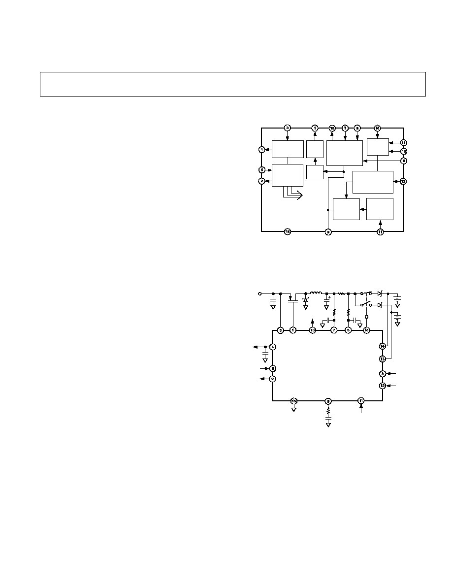
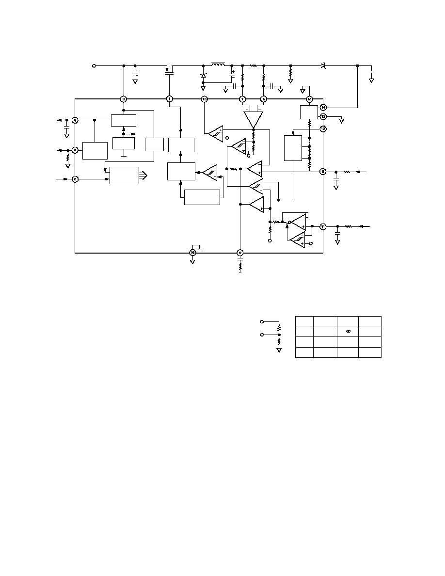
FUNCTIONAL BLOCK DIAGRAM
ADP3801/ADP3802
LDO +
REFERENCE
A/B
SELECT
MUX
DRV
VCC
CS+ CS
A/B
PROG
ADJ
COMP
GND
SD
VL
RESET
ISET
BATB
BATA
EOC
SD
\UVLO
GATE
DRIVE
CURRENT
LOOP
AMP + EOC
COMPARATOR
PWM
FINAL BATTERY
VOLTAGE
PROGRAM
(4.2, 8.4, 12.6)
VOLTAGE
LOOP
AMP
BATTERY
VOLTAGE
ADJUST
10%
SHUTDOWN
UVLO
+
RESET
FEATURES
Stand-Alone Li-Ion Battery Chargers
High End-of-Charge Voltage Accuracy
0.4% @ +25 C
0.75% @ 10 C to +70 C
Intelligent End-of-Charge Output Signal
Pin Programmable Cell Number Select
On Chip 3.3 V LDO Regulator
Programmable Charge Current with High Side Sense
Softstart Charge Current
Undervoltage Lockout
Drives External PMOS
10% Adjustable End-of-Charge Voltage
Charges NiCad, NiMH (with External Controller)
PWM Oscillator Frequency:
ADP3801: 200 kHz
ADP3802: 500 kHz
APPLICATIONS
Fast Chargers
Universal Chargers
Cellular Phones
Portable Computers
Portable Instrumentation
Desktop Chargers
Personal Digital Assistants
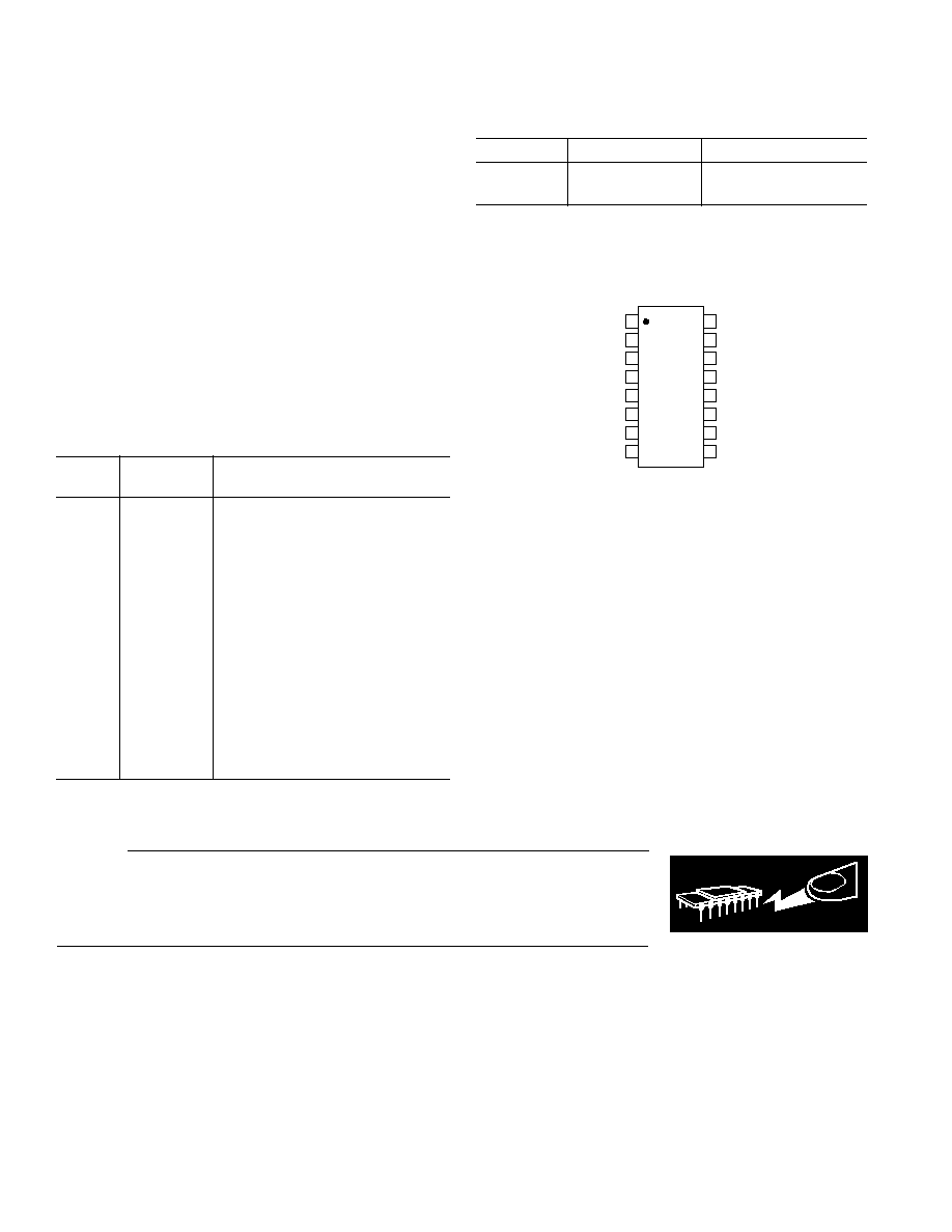
GENERAL DESCRIPTION
The ADP3801 and ADP3802 are complete battery charging
ICs. The devices combine a high accuracy final battery voltage
control with a constant charge current control and an on-board
Low Drop-Out Regulator (LDO). The accuracy of the final
battery voltage control is guaranteed to
±
0.75% to safely charge
Li-Ion batteries. An internal multiplexer allows the alternate
charging of two separate battery stacks. The final voltage is pin
programmable to one of three Li-Ion options: 4.2 V (one Li-Ion
cell), 8.4 V (two Li-Ion cells), or 12.6 V (three Li-Ion cells).
Paired with an external microcontroller for charge termination,
the ADP3801/ADP3802 works as a fast charger for NiCad/
NiMH batteries or as a universal charger for all three battery
chemistries. In addition, a pin is provided for changing the final
battery voltage by up to
±
10% to adjust for variations in battery
chemistry from different Li-Ion manufacturers without loss of
accuracy in the final battery voltage.
BATA
BATB
VCC DRV
EOC
CS
CS+
ISET
BATA
ADJ
GND
RESET
V
IN
VL
ADP3801/ADP3802
SD
BATB
3.3V
40m
A/B
COMP
PROG
68 H
Figure 1. 4 Amp Dual Battery Charger

2
REV. 0
ADP3801/ADP3802SPECIFICATIONS
Parameter
Conditions
Symbol
Min
Typ
Max
Units
FINAL BATTERY VOLTAGE
One Li-Ion Cell
PROG = V
T1
, ADJ = VL, T
A
= +25
°
C
V
BAT
4.180
4.200
4.220
V
PROG = V
T1
, ADJ = VL, 10
°
C
T
A
+70
°
C V
BAT
4.168
4.232
V
PROG = V
T1
, ADJ = VL, 40
°
C
T
A
+85
°
C V
BAT
4.150
4.250
V
Two Li-Ion Cells
1
PROG = V
T2
, ADJ = VL, T
A
= +25
°
C
V
BAT
8.366
8.400
8.434
V
PROG = V
T2
, ADJ = VL, 10
°
C
T
A
+70
°
C V
BAT
8.337
8.463
V
PROG = V
T2
, ADJ = VL, 40
°
C
T
A
+85
°
C V
BAT
8.300
8.500
V
Three Li-Ion Cells
1
PROG = V
T3
, ADJ = VL, T
A
= +25
°
C
V
BAT
12.550
12.600
12.650
V
PROG = V
T3
, ADJ = VL, 10
°
C
T
A
+70
°
C V
BAT
12.505
12.695
V
PROG = V
T3
, ADJ = VL, 40
°
C
T
A
+85
°
C V
BAT
12.450
12.750
V
BATTERY PROGRAMMING
INPUT (PROG)
One Li-Ion Cell
(4.2 V)
V
T1
0.00
0.20
V
Two Li-Ion Cells
(8.4 V)
V
T2
1.00
1.20
V
Three Li-Ion Cells
(12.6 V)
V
T3
2.05
2.30
V
Fail Safe Voltage
(4.2 V)
Defaults to 1 Li-Ion Cell
3.10
3.30
V
PROG Input Current
I
B
1.5
5
µ
A
A/B SELECT MUX
Select Battery BATB
V
IH
2.0
V
Select Battery BATA
V
IL
0.8
V
A/B Input Current
I
IN
0.02
1
µ
A
BATA or BATB Input Resistance
Channel Selected
R
IN
185
265
k
BATA or BATB Input Current
Channel Not Selected
I
BA
, I
BB
0.2
1
µ
A
BATA or BATB Shutdown Current Part in Shutdown
I
BA
, I
BB
0.2
1
µ
A
BATTERY ADJUST INPUT
2
(ADJ)
% of Final Battery Voltage
ADJ = 1.0 V, 10
°
C
T
A
+70
°
C
89
90
91
%
% of Final Battery Voltage
ADJ = 2.3 V, 10
°
C
T
A
+70
°
C
109
110
111
%
ADJ Disable Voltage Threshold
0% Change
2.475
2.6
V
ADJ Bias Current
1.0 V
ADJ
2.3 V
I
B
10
100
nA
OVERVOLTAGE COMPARATOR
Trip Point
Percent Above V
BAT
8
%
Response Time
DRV Goes High
tr
2
µ
s
OSCILLATOR
200 kHz Option
(ADP3801)
f
OSC
150
200
250
kHz
500 kHz Option
(ADP3802)
f
OSC
375
500
625
kHz
0% Duty Cycle Threshold
@ COMP Pin
1.0
V
100% Duty Cycle Threshold
@ COMP Pin
2.0
V
GATE DRIVE
Rise Time
C
L
= 1 nF, VCC 4 V to 90%
t
r
35
ns
Fall Time
C
L
= 1 nF, 90% to VCC 4 V
t
f
75
ns
Output High Saturation Voltage
VCC V
DRV
V
OH
275
mV
Output Low Voltage
VCC = 8 V
V
OL
1.0
2.0
V
VCC > 8 V
V
OL
VCC 7 VCC 6
V
CURRENT SENSE AMPLIFIER
Input Common-mode Range
V
CS+
and V
CS
V
CSCM
0.0
VCC 2
V
Input Differential Mode Range
V
CS
3
V
CSDM
0.0
185
mV
Input Offset Voltage
4
0.0 V
V
CSCM
VCC 2 V
V
CSVOS
1
mV
Input Bias Current
0.0 V
V
CSCM
VCC 2 V
V
CSIB
0.3
1
µ
A
Input Offset Current
0.0 V
V
CSCM
VCC 2 V
V
CSIOS
0.01
0.15
µ
A
Over Current Trip Point
V
CS
3
185
mV
Response Time
DRV Goes High
tr
2
µ
s
ISET INPUT
Charge Current Programming
Function
0.0 V
V
ISET
1.65 V
V
CS
/V
ISET
3
0.1
V/V
Programming Function Accuracy
V
ISET
= 1.65 V, 10
°
C
T
A
+70
°
C
5
±
1.0
+5
%
V
ISET
= 0.10 V, 10
°
C
T
A
+70
°
C
25
±
10
+25
%
ISET Bias Current
0.0 V
V
ISET
1.65 V
I
B
15
100
nA
(@ 40 C
T
A
+85 C, VCC = 10.0 V, unless otherwise noted)

3
REV. 0
ADP3801/ADP3802
Parameter
Conditions
Symbol
Min
Typ
Max
Units
EOC OUTPUT
5
Trip Point
100 k
to VL
V
CS
3
10
mV
Hysteresis
100 k
to VL
V
CS
3
0.2
mV
SHUTDOWN (SD)
ON
SD
H
2.0
V
OFF
SD
L
0.8
V
SD Input Current
0.2
1
µ
A
LOW DROPOUT REGULATOR
Output Voltage
6
0 mA
I
LOAD
10 mA,
4.1 V
VCC
20 V, 10
°
C
T
A
+70
°
C
VL
3.267
3.3
3.333
V
0 mA
I
LOAD
10 mA,
4.1 V
VCC
20 V, 40
°
C
T
A
+85
°
C
VL
3.250
3.350
V
Dropout Voltage (VCC VL)
I
LOAD
= 10 mA
V
DO
0.4
0.8
V
Output Current Drive
I
VL
10
20
mA
RESET OUTPUT
VL Rising Threshold
RESET High
2.5
2.7
2.9
V
VL Falling Threshold
RESET Low
2.4
2.55
2.8
V
Output High Logic Level
1 M
to Ground External
2.4
2.9
V
POWER SUPPLY
ON Supply Current
No External Loads
I
SYON
5.0
7.0
mA
OFF Supply Current
No External Loads
I
SYOFF
115
180
µ
A
UVLO
6, 7
VCC Rising Threshold
Turn On
3.8
3.9
4.0
V
VCC Falling Threshold
Turn Off, I
VL
= 1 mA
3.4
V
NOTES
1
VCC
= V
BAT
+ 2 V.
2
See Figure 5.
3
V
CS
= (V
CS+
) (V
CS
).
4
Accuracy guaranteed by ISET
INPUT, Programming Function Accuracy specification.
5
EOC Output Comparator monitors charge current, and it is enabled when V
BAT
95% of the final battery voltage.
6
LDO is active during SD and UVLO.
7
Turn-off threshold depends on LDO dropout.
All limits at temperature extremes are guaranteed via correlation using standard Statistical Quality Control (SQC) methods.
Specifications subject to change without notice.
ADP3801/ADP3802
4
REV. 0
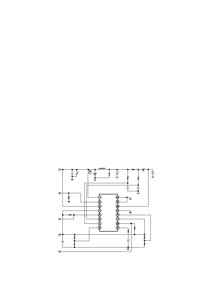
PIN CONFIGURATION
TOP VIEW
(Not to Scale)
16
15
14
13
12
11
10
9
1
2
3
4
5
6
7
8
DRV
VL
SD
CS
CS+
ISET
GND
A/B
BATA
BATB
PROG
ADJ
EOC
COMP
ADP3801
ADP3802
VCC
RESET
ABSOLUTE MAXIMUM RATINGS*
Input Voltage (VCC to GND) . . . . . . . . . . . . . . 0.3 V to 20 V
DRV, V
CS+
, V
CS
to GND . . . . . . . . . . . . . . . . 0.3 V to VCC
BATA, BATB to GND . . . . . . . . . . . . . . . . . 0.3 V to 14.0 V
A/B, ISET, PROG, ADJ to GND . . . . . . . . . . . 0.3 V to VL
SD, RESET, COMP, EOC to GND . . . . . . . . . . 0.3 V to VL
Power Dissipation . . . . . . . . . . . . . . . . . . . . Internally Limited
JA
. . . . . . . . . . . . . . . . . . . . . . . . . . . . . . . . . . . . . 75
°
C/W
Ambient Temperature Range . . . . . . . . . . . . 40
°
C to +85
°
C
Storage Temperature Range . . . . . . . . . . . . 65
°
C to +150
°
C
Lead Temperature Range (Soldering 10 sec) . . . . . . . +300
°
C
NOTES
*This is a stress rating only and functional operation of the device at these or any
other conditions above those indicated in the operation section of this specification
is not implied. Exposure to absolute maximum rating conditions for extended
periods may affect device reliability.
JA
is specified for worst case conditions with device soldered on a circuit board.
ORDERING GUIDE
Model
Package Option
Oscillator Frequency
ADP3801AR
R-16A
200 kHz
ADP3802AR
R-16A
500 kHz
CAUTION
ESD (electrostatic discharge) sensitive device. Electrostatic charges as high as 4000 V readily
accumulate on the human body and test equipment and can discharge without detection. Although
the ADP3801/ADP3802 features proprietary ESD protection circuitry, permanent damage may
occur on devices subjected to high energy electrostatic discharges. Therefore, proper ESD precau-
tions are recommended to avoid performance degradation or loss of functionality.
WARNING!
ESD SENSITIVE DEVICE
PIN FUNCTION DESCRIPTIONS
Pin
Number
Mnemonic
Function
1
DRV
External Transistor Drive
2
RESET
Power on RESET Output
3
VCC
Supply Voltage
4
VL
LDO Output
5
SD
Shutdown Control Input
6
CS
Negative Current Sense Input
7
CS+
Positive Current Sense Input
8
ISET
Charge Current Program Input
9
COMP
External Compensation Node
10
EOC
End-of-Charge Output Signal
11
ADJ
Adjust Battery Voltage
±
10%
12
PROG
Program Final Battery Voltage Input
13
BATB
Battery "B" Voltage Sense
14
BATA
Battery "A" Voltage Sense
15
A/B
1
"A" or "B" Battery Select Input
16
GND
Ground
NOTE
1
"L" = Battery "A."
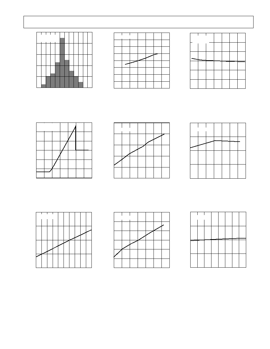
Typical Performance CharacteristicsADP3801/ADP3802
5
REV. 0
V
BAT
ACCURACY %
TOTAL NUMBEROF PARTS
0
0.5
20
0.4
0.3
0.1
0.1
0.3
0.5
0.2
0
0.2
0.4
0.6
40
60
80
100
VCC = 10V
T
A
= +25 C
Figure 2. V
BAT
Accuracy Distribution
V
ADJ
Volts
V
BAT
PERCENT CHANGE %
0
0.5
1.0
1.5
2.0
3.0
3.5
15
10
5
0
5
10
15
2.5
VCC = 10V
T
A
= +25 C
Figure 5. V
BAT
Percent Change vs. V
ADJ
LDO LOAD CURRENT mA
UVLO TRIP POINT Votts
0
1
2
3
4
6
7
3.3
3.4
3.5
3.6
3.7
5
8
9
10
T
A
= +25 C
Figure 8. UVLO Trip Point-Off vs.
LDO Load Current
TEMPERATURE C
V
BAT
ACCURACY %
0.4
40
VCC = 10V
20
0
20
40
60
80
100
0.3
0.2
0.1
0
0.1
0.2
0.3
0.4
Figure 3. V
BAT
Accuracy vs.
Temperature
TEMPERATURE C
THRESHOLD %
40
20
0
20
40
80
100
6
7
8
9
10
60
VCC = 10V
5
Figure 6. Overvoltage Comparator
Threshold vs. Temperature
TEMPERATURE C
LDO ACCURACY %
40
0.3
0.2
0.1
0
0.1
0.3
0.2
20
0
20
40
60
80
100
VCC = 10V
Figure 9. LDO Accuracy vs.
Temperature
SUPPLY VOLTAGE Volts
V
BAT
ACCURACY %
T
A
= +25 C
V
BAT
= 4.2V
6
8
10
12
14
18
20
0.3
0.2
0.1
0
0.1
0.2
0.3
16
Figure 4. V
BAT
Accuracy vs. Supply
Voltage
TEMPERATURE C
THRESHOLD mV
40
20
0
20
40
80
100
180
185
190
195
200
60
VCC = 10V
Figure 7. Overcurrent Comparator
Threshold vs. Temperature
SUPPLY VOLTAGE Volts
LDO ACCURACY %
4
6
8
10
12
16
18
0
0.1
0.2
14
20
T
A
= +25 C
0.2
0.1
Figure 10. LDO Accuracy vs. Supply
Voltage
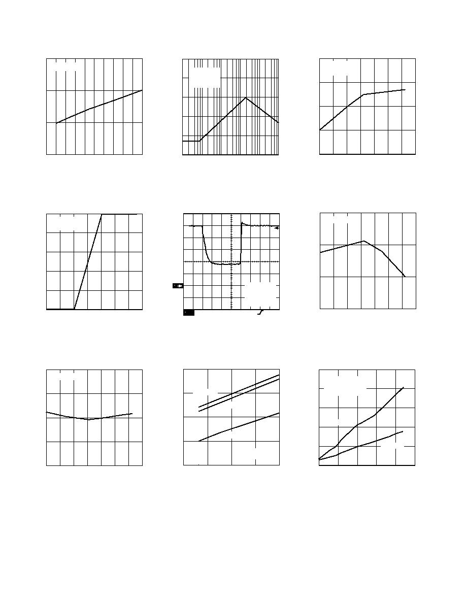
ADP3801/ADP3802
6
REV. 0
LOAD CURRENT mA
DROPOUT VOLTAGE Volts
0
1
2
3
4
6
7
5
8
T
A
= +25 C
0.1
9
10
0.2
0.3
0.4
Figure 11. LDO Dropout Voltage vs.
Load Current
V
COMP
Volts
DUTY CYCLE %
0
0.5
2.0
2.5
3.0
0
20
40
60
80
3.5
VCC = 10V
T
A
= +25 C
1.5
1.0
100
Figure 14. Duty Cycle vs. COMP Pin
Voltage
TEMPERATURE C
CLAMP VOLTAGE Volts
40
20
40
60
80
3.6
3.7
100
VCC = 10V
20
0
3.8
3.5
3.9
Figure 17. DRV Output Low Voltage
with VCC = 10 V vs. Temperature
FREQUENCY Hz
PSRR dB
100
1.0E+01
80
60
40
20
0
1.0E+02 1.0E+03 1.0E+04 1.0E+05 1.0E+06
VCC = 10V
T
A
= +25 C
C
LDO
= 1 F
Figure 12. LDO PSRR vs. Frequency
1
TIME ns
DRV Volts
2.00V
12
8
6
4
2
0
9.40V
CH1
M 250ns
VCC = 10V
C
L
= 1nF
T
A
= +25 C
250ns/DIV
CH1
10
Figure 15. DRV Rise and Fall Times
SUPPLY VOLTAGE Volts
POWER SUPPLY CURRENT mA
4
8
16
4.0
4.5
20
T
A
= +85 C
12
5.0
3.5
5.5
T
A
= +25 C
T
A
= 40 C
NOT SWITCHING
SD
= ON
Figure 18. Power Supply Current vs.
Supply Voltage @ Three Temperatures
TEMPERATURE C
FREQUENCY kHz
40
20
0
20
40
80
100
60
VCC = 10V
ADP3801
175
185
195
215
205
Figure 13. Oscillator Frequency vs.
Temperature
SATURATION VOLTAGE Volts
40
20
40
60
80
0
0.2
100
VCC = 10V
20
0
0.4
0.3
TEMPERATURE C
Figure 16. DRV High Saturation Volt-
age vs. Temperature
CAPACITIVE LOAD nF
POWER SUPPLY CURRENT mA
0
0.5
1.5
9
11
2.0
1.0
13
7
15
5
2.5
ADP3801
ADP3802
VCC = 10V
T
A
= +25 C
50% DUTY CYCLE
Figure 19. Power Supply Current vs.
Capacitive Load on DRV

ADP3801/ADP3802
7
REV. 0
APPLICATIONS SECTION
PRODUCT DESCRIPTION
The ADP3801 and ADP3802 are complete Li-Ion battery charg-
ing ICs. Combined with a microcontroller, they also function as
voltage limited,
µ
C programmable constant current source chargers
for NiCad and NiMH chemistries. Utilizing an external PMOS
pass transistor, the devices realize a buck type constant current,
constant voltage (CCCV) charger controller that is capable of
charging two separate battery packs for such applications as
portable computer chargers and cellular phone chargers. The
Functional Block Diagram shows the ICs' functional blocks,
which are detailed below:
· A/B SELECT MUX--Two-channel multiplexer for charging
two battery stacks.
· FINAL BATTERY VOLTAGE PROGRAM--Multiplexer to
program 4.2 V, 8.4 V, or 12.6 V final battery voltage.
· VOLTAGE LOOP AMP--GM-type amplifier to control
the final battery voltage. It includes a built-in overvoltage
comparator.
· EOC COMPARATOR--End-of-charge detection output to
signal when the battery is fully charged.
· BATTERY VOLTAGE ADJUST--Amplifier to adjust the
final battery voltage up to
±
10%.
· CURRENT LOOP AMP--High-side-current-sense amplifier
to sense and control the charge current at a programmable
level. It includes an overcurrent comparator.
· PWM--Pulsewidth modulator and oscillator (ADP3801-
200 kHz, ADP3802-500 kHz).
· GATE DRIVE--Gate drive to control an external pass tran-
sistor. It includes a clamp to limit the drive voltage to protect
the external PMOS.
· LDO + REFERENCE--3.3 V low dropout regulator to sup-
ply an external microcrontroller and for on-chip supply. In-
cludes an internal precision reference ( VREF = VL/2).
· SHUTDOWN--Logic input to shut down the charger. The
LDO remains on.
· UVLO--Undervoltage lockout circuit to shut down the charger
for low supply voltages.
· RESET--Active LOW output to reset external logic on power-
up.
During charging, the ADP3801/ADP3802 maintains a constant,
programmable charge current. The high side current sense
amplifier has low offset allowing the use of a low voltage drop
for current sensing: 165 mV for the maximum charge current.
The input common-mode range extends from ground to
VCC 2 V ensuring current control over the full charging volt-
age of the battery, including a short circuit condition. A high
impedance dc voltage input (ISET) is provided for program-
ming the charge current over a wide range. When the battery
voltage approaches its final limit, the part automatically trans-
fers to voltage control mode. Both the current control loop and
the voltage control loop share the same compensation pin mini-
mizing the number of external components. An internal com-
parator monitors the charge current to detect the end-of-charge
(EOC). When the current decreases such that V
CS
8 mV, the
EOC output pulls low.
A 3.3 V LDO is used to generate a regulated supply for internal
circuitry. Additionally, the LDO can deliver up to 10 mA of
current to power external circuitry such as a microcontroller. An
Undervoltage Lockout (UVLO) circuit is included to safely shut
down the charging circuitry when the input voltage drops below
its minimum rating. A shutdown pin is also provided to turn off
the charger when, for example, the battery has been fully charged.
The LDO remains active during shutdown or UVLO and has a
quiescent current of 110
µ
A.
Battery Charging Overview
Figure 20 shows a simplified Buck type battery charger applica-
tion circuit for the ADP3801/ADP3802. When a discharged
battery is first placed in the charger, the battery voltage is well
below the final charge voltage, so the current sense amplifier
controls the charge loop in constant current mode. The charge
current creates a voltage drop across the sense resistor R
CS
. This
voltage drop is buffered and amplified by amplifier GM1. Am-
plifier GM2 compares the output of GM1 to an external current
control voltage provided at the ISET pin and servos the charger
loop to make these voltages equal. Thus, the charge current is
programmed using the ISET input voltage.
The output of GM2 is analog "OR'ed" with the output of GM3,
the voltage loop amplifier. Only one or the other amplifier con-
trols the charge loop at any given time. As the battery voltage
approaches its final voltage, GM3 comes into balance. As this
occurs, the charge current decreases, unbalancing GM2, and
control of the feedback loop naturally transfers to GM3.
The ADP3801/ADP3802 can control the charging of two inde-
pendent battery stacks or a single battery stack. The A/B SELECT
MUX has a logic input to choose between the two batteries. See
Figure 31 for more information on dual battery charging. The
output of the multiplexer is applied to a precision thin-film
resistor string to divide down the battery voltage. The final
battery voltage is chosen by selecting the proper resistor divider
tap with the PROG multiplexer. The output of this mux goes
directly to the input of GM3, comparing the divided down
battery voltage to the internal reference. To guarantee
±
0.75%
accuracy, a high precision internal reference and high accuracy
thin film resistors are used. Including these components on-
chip saves the significant cost and design effort of adding them
externally.
ADP3801/ADP3802
8
REV. 0
BIAS
LDO
RESET
GATE
DRIVE
FF
VI
N
CS+
OSCILLATOR
D1
L
R
CS
V
REF
3.3V
UVLO
S
R
BATA
ISET
A/B
CS
(FROM C)
Rf2
Rf1
COMP
1 F
V
REF
POWER-
ON
RESET
(FROM C)
(TO C)
(TO C)
FINAL
VBAT
PROG
GND
MUX
PROG
(FROM C)
2.475V
ADJ
VCC
V
REF
3R
DRV
VL
D2
RB
SD
BATA
1 F
CI
N
COUT
EOC
Q
VT
ADP3801/ADP3802
100k
BATB
GM1
GM2
GM3
R
100k
V
REF
Figure 20. Simplified Application Diagram
Setting the Final Battery Voltage
The final battery voltage is determined by the voltage on the
Battery Programming (PROG) pin. This pin controls the state
of the PROG multiplexer, which selects the appropriate tap
from the internal battery voltage resistor divider. The specifica-
tion table details the PROG voltages for each final battery volt-
age. A resistor divider from the LDO can be used to set the
PROG voltage as shown in Figure 21. To provide fail safe op-
eration, a PROG voltage equal to 0.0 V or 3.3 V results in the
minimum final battery voltage of 4.2 V. The PROG input is
high impedance, so the voltage can be set with a high imped-
ance resistor divider from VL. Alternatively, a PWM output
from a microcontroller can be used with an RC filter to generate
the desired threshold voltage.
VL
R1
4.2
V
T1
= 0.0V
0*
8.4
V
T2
= 1.1V
200k
100k
12.6
V
T3
= 2.2V
100k
200k
V
BAT
SETTING
R1 (5%)
R2 (5%)
R2
PROG
* CONNECT PROG TO
GND FOR V
BAT
= 4.2V
Figure 21. Resistor Divider Sets the Final Battery Voltage

ADP3801/ADP3802
9
REV. 0
Adjusting the Final Battery Voltage
In addition to the PROG input, the ADP3801/ADP3802 pro-
vides an input (ADJ) for fine adjustment of the final battery
voltage. For example, the ADJ amplifier allows the nominal
4.2 V per cell setting for Li-Ion battery cells to be adjusted to
4.1 V for certain chemistries. An internal amplifier buffers the
ADJ pin and adjusts the internal reference voltage on the input
to GM3. Figure 5 shows a graph of the percent change in final
battery voltage vs. the ADJ voltage. The linear portion between
0.6 V
REF
and 1.4 V
REF
follows the formula below:
V
V
V
V
BAT
AD
REF
REF
%
( )
=
-
×
J
4
100
The factor of four in the denominator is due to internal scaling.
When V
ADJ
is above 2.5 V, an internal comparator switches off
the ADJ amplifier, giving a 0% change in V
BAT
. Whenever the
ADJ function is not used it should be connected to VL.
The total range of adjustment is
±
10%. For example, the 4.2 V
final battery voltage setting can be adjusted from 3.78 V to
4.62 V. Of course, care must be taken not to adjust the final
battery voltage to an unsafe charging level for Li-Ion batteries.
Follow the battery manufacturers specifications for the appro-
priate final battery voltage. Never charge a Li-Ion battery above
the manufacturers rated maximum!
Voltage Loop Accuracy
The ADP3801/ADP3802 guarantees that the battery voltage be
within
±
0.75% of the setpoint over the specified temperature
range and the specified charge current range. This inclusive
specification saves the designer the time and expense of having
to design-in additional high accuracy components such as a
reference and precision resistors.
To maintain the
±
0.75% specification, the layout and design of
the external circuitry must be considered. The input impedance
of BATA and BATB is typically 265 k
, so any additional im-
pedance on these inputs will cause an error. As a result, do not
add external resistors to the battery inputs. Furthermore, if the
output voltage is being used for other purposes, such as to sup-
ply additional circuitry, the current to this circuitry should be
routed separately from the sense lines to prevent voltage drops
due to impedance of the PC-board traces. In general, route the
sense lines as Kelvin connections as close to the positive termi-
nals of the battery as possible.
The same care must be given to the ground connection for the
ADP3801/ADP3802. Any voltage difference between the bat-
tery ground and the GND pin will cause an error in the charge
voltage. This error includes the voltage drop due to the ground
current of the part. Thus, the GND pin should have a thick
trace or ground plane connected as close as possible to the
battery's negative terminal. Any current from additional cir-
cuitry should be routed separately to the supply return and not
share a trace with the GND pin.
Dual Battery Operation
The ADP3801/ADP3802 is designed to charge two separate
battery packs. These batteries can be of different chemistries
and have a different number of cells. At any given time, only
one of the two batteries is being charged. To select which bat-
tery is being monitored, and therefore which battery is being
charged, the ADP3801/ADP3802 includes a battery selector
mux. This two-channel mux is designed to be "break-before-
make" to ensure that the two batteries are not shorted together
momentarily when switching from one to the other. The A/B
input is a standard logic input, with a logic low selecting BATA
and a logic high selecting BATB. See the application in Figure
31 for more information.
Overvoltage Comparator
GM3 includes an overvoltage comparator. Its output bypasses
the COMP node to quickly reduce the duty cycle of the PWM
to 0% when an overvoltage event occurs. A second output is
connected to the COMP node and, with slower response, re-
duces the voltage on the COMP cap to provide a soft start re-
covery. The threshold of the comparator is typically 8% above
the final battery voltage. This comparator protects external
circuitry from any condition that causes the output voltage to
quickly increase. The most likely reason is if the battery is
suddenly removed while it is being charged with high current.
Figure 27 shows the transient response when the battery is
removed. Notice that the output voltage increases to the com-
parator trip point, but it is quickly brought under control and
held at the final battery voltage.

ADP3801/ADP3802
10
REV. 0
Current Sense Amplifier
A differential, high side current sense amplifier (GM1 in Figure
20) amplifies the voltage drop across a current sense resistor
R
CS
. The input common-mode range of GM1 extends from
ground to VCC 2 V. Sensing to ground ensures current regu-
lation even in short circuit conditions. To stay within the com-
mon-mode range of GM1, VCC must be at least 2 V greater
than the final battery voltage or a circuit such as shown in Fig-
ure 32 must be used. RC filters are included to filter out high
frequency transients, which could saturate the internal circuitry.
The filter's cutoff is typically set at half the switching frequency
of the oscillator.
The charge current is controlled by the voltage on the ISET pin
according to the following formula:
I
V
R
CHARGE
ISET
CS
=
×
10
The factor of 10 is due the GM1's gain of 10 V/V. To set a charge
current of 1.5 A with R
CS
= 0.1
, V
ISET
must be 1.5 V. Figure
22 shows the linearity of the charge current control as the volt-
age is increased from 0 V to the programmed final battery volt-
age (12.6 V in this case). It is important to state that this curve
is taken with an ideal, zero impedance load. An actual Li-Ion
battery will exhibit a more gradual drop in charge current due to
the internal impedance of the battery as shown in Figure 25.
V
OUT
Volts
0
2
3
I
CHARGE
Amps
4
5
6
7
8
9
10
0.5
11
12
13
1.0
1.5
2.0
2.5
3.0
3.5
Figure 22. CCCV Characteristic with Ideal Load
Overcurrent Comparator
Similar to the voltage loop, the current loop includes a com-
parator to protect the external circuitry from an overcurrent
event. This comparator trips when GM1's differential input
voltage exceeds 185 mV. Like the overvoltage comparator, it has
two outputs to quickly reduce the duty cycle to 0% and to pro-
vide a soft-start recovery. The response time of the internal
comparator is approximately 1
µ
s; however, the filter on the
input of GM1 may slow down the total response time of the
loop.
End-of-Charge Output
The ADP3801/ADP3802 provides an active low, end-of-charge
(EOC) logic output to signal when the battery has completed
charging. The typical Li-Ion charging characteristic in Figure 25
shows that when the battery reaches its final voltage the current
decreases. To determine EOC, an internal comparator senses
when the current falls below 6% of full scale, ensuring that the
battery has been fully charged. The comparator has hysteresis to
prevent oscillation around the trip point.
To prevent false triggering (such as during soft-start), the com-
parator is only enabled when the battery voltage is within 5% of
its final voltage. As the battery is charging up, the comparator
will not go low even if the current falls below 6% as long as the
battery voltage is below 95% of full scale. Once the battery has
risen above 95%, the comparator is enabled.
There are two important reasons for this functionality. First,
when the circuit is initially powered on, the charge current is
zero because of the soft start. If the comparator is not gated by
the battery voltage, then EOC would go low erroneously. Sec-
ond, a provision must be made for battery discharge. Assume
that a battery has been fully charged. EOC goes low, and the
charger is gated off. When the battery voltage falls to 95%, due
to self-discharge for example, EOC will return high. Then the
charger can start up and top off the battery, preventing the
battery from "floating" at the end-of-charge voltage.
The EOC output has many possible uses as shown in Figure 23.
One simple function is to terminate the charging to prevent
floating (Figure 23a). It can be used as a logic signal to a
microcontroller to indicate that the battery has finished charg-
ing. The microcontroller can then switch to the next battery if
appropriate or shutdown the ADP3801/ADP3802. It can also be
used to turn on an LED to signal charge completion (Figure
23b). Using a flip-flop, EOC can control the switching from
BATA to BATB (Figure 23d). The RC filter delays switching
between the two batteries to ensure that the output capacitor is
discharged.
ADP3801/ADP3802
11
REV. 0
ADP3800
COMP
EOC
(a) EOC Output Terminates Charge
270
2N3906
ADP3800
EOC
VL
100k
0.1 F
(b) EOC Turns on LED to Signal Charge Completion
2N3904 2
ADP3800
EOC
VL
COMP
100k
100k
2N3906
0.1 F
10k
20k
20k
270
(c) EOC Terminates Charge and Turns on LED
100k
ADP3800
EOC
*LEVEL SHIFTED TO
TO DRIVE PMOS
VL
100k
100k
2N3906
1 F
COMP
RESET
J
K
Q
Q
74H73A
BATSELB*
A/B + BATSELA*
100k
0.1 F
20k
2N3904 2
10k
(d) Flip-Flop Switches Between Batteries on EOC Signal
Figure 23. EOC Output Circuits
COMP Node
Both the current loop and the voltage loop share a common,
high impedance compensation node, labeled COMP. A series
capacitor and resistor on this node help to compensate both
loops. The resistor is included to provide a zero in the loop
response and boost phase margin.
The voltage at the COMP node determines the duty cycle of the
PWM. The threshold levels are typically 1.0 V for 0% duty cycle
and 2.0 V for 100% duty cycle, resulting in a total range of
1.0 V. When the ADP3801/ADP3802 first turns on, the COMP
capacitor is at 0.0 V. It has to charge up to at least 1.0 V before
the duty cycle rises above 0% and the pass transistor turns on.
This "soft-start" behavior is desirable to avoid undue stress on
the external components. In addition, whenever the part is
placed in Shutdown or in UVLO, the COMP capacitor is dis-
charged to ensure soft start upon recovery.
The current available to charge and discharge the COMP ca-
pacitor during normal operation is 100
µ
A. Thus, the slew rate
at this node is equal to 100
µ
A divided by the capacitor. For a
typical capacitance of 1
µ
F, the slew rate is 0.1 V/ms. Thus, it
takes about 10 ms before the ADP3801/ADP3802 starts to
operate from a soft-start state. This is regardless of the internal
oscillator frequency. One important note is that the COMP
node is a high impedance point. Any external resistance or leak-
age current on this node will cause an error in both the charge
current control and the final battery voltage.
Gate Drive
The ADP3801/ADP3802 gate drive is designed to provide high
transient currents to drive the pass transistor. The rise and fall
times are typically 20 ns and 200 ns respectively when driving
a 1 nF load, which is typical for a PMOSFET with R
DS(ON)
=
60 m
. Figure 15 shows the typical transient response of the
output stage driving this load from a 10 V supply.
A voltage clamp is added to limit the pull-down voltage to 7 V
below VCC. For example, if VCC is 10 V then the output will
pull down to 3 V minimum, limiting the V
GS
voltage applied to
the external FET.
Low Dropout Regulator and Reference
A 3.3 V LDO is used to generate a regulated supply for internal
circuitry. Additionally, the LDO can deliver up to 10 mA of
current to power external circuitry such as a microcontroller. A
1.0
µ
F capacitor must be placed close to the VL pin to ensure
stability of the regulator. Due to the design of the regulator,
stability is not contingent on the ESR for the output capacitor.
Many different types of capacitors can be used providing flex-
ibility and ease of design. The LDO also includes a high accu-
racy, low drift internal reference equal to half of VL to set levels
within the part. During shutdown and UVLO, both the refer-
ence and the LDO remain active.
Shutdown
The IC may be placed in shutdown at any time to stop charging
of the batteries and to conserve power. For example, to safely
switch from one battery to the next, the part should be shut
down to momentarily interrupt charging. Also, if the batteries
have completed charging or no batteries are present, then the
part may be placed in shutdown to save power. A logic low on
ADP3801/ADP3802
12
REV. 0
SD results in shutdown. All internal circuitry is shut off except
for the LDO and the reference, and the supply current is typi-
cally 110
µ
A. When SD returns high, the part resumes full op-
eration. The compensation capacitor at the COMP node is
discharged during shutdown, so the part will resume operation
in soft-start mode.
Undervoltage Lockout--UVLO
The internal Undervoltage Lockout (UVLO) circuit monitors
the input voltage and keeps the part in shut-down mode until
VCC rises above 3.9 V. During UVLO, the LDO and reference
are still active, but the analog front end, the oscillator, and the
gate drive are off. UVLO helps to prevent the circuitry from
entering an unknown state that could incorrectly charge a battery.
To prevent oscillation around VCC = 3.9 V, the UVLO cir-
cuitry has built-in hysteresis. Once the part is on, the UVLO
circuitry does not shut it off until the LDO enters dropout.
Because the dropout voltage depends on the LDO's load, the
UVLO trip point-off also depends on the load. Refer to Figure 8
for a graph of the UVLO trip point-off versus LDO load.
RESET
When the power is first applied to the ADP3801/ADP3802, the
RESET pin is held at ground by an external 1 M
resistor. It
remains low until the LDO output voltage rises to above 80% of
its final value. When this threshold is reached, the RESET pin is
pulled high. The internal RESET comparator includes about
150 mV of hysteresis to avoid oscillation around the threshold.
Supply Considerations
The guaranteed operating supply voltage range of the ADP3801/
ADP3802 is from 4 V to 20 V, and it typically consumes 5.0 mA
of quiescent current when not switching. However, the part
needs at least 2 V of headroom between VCC and the voltage
on the CS+ and CS pins. This is for the common-mode range
on the current sense amplifier. In applications where the input
supply does not offer enough headroom, the circuits in Figures
32 and 33 can be used as explained in the section on low over-
head charging.
Overtemperature Shutdown
The ADP3801/ADP3802 has an on-chip temperature detector
to shut the part down when the die temperature reaches typi-
cally +160
°
C. Such a condition could occur with a short-circuit
on the LDO or a short on the DRV pin. In either case, the op-
eration of the charger will stop and the DRV pin will be pulled
high. With approximately +10
°
C hysteresis, the overtemperature
shutdown releases at typically +150
°
C. These temperatures are
higher than the absolute maximum ratings for the die, and are
included as a safety feature only.
Li-Ion Battery Charger
The ADP3801 and ADP3802 are ideally suited for a single or
dual Li-Ion batterypack charger. They combine 200 kHz or
500 kHz switching with a PMOS pass transistor drive to realize
a Buck topology CCCV charger. The following discussion goes
through the complete design of a charger using the ADP3801.
This information also applies to the ADP3802.
Charger Specifications
Battery: 3 Series Cell Li-Ion Pack.
Input Voltage: V
IN
= 15 V dc to 20 V dc.
Final Battery Voltage: V
BAT
= 12.6 V.
Charge Current: I
CHARGE
= 4.0 A (for V
O
= 0 V to 12.6 V)
Circuit Topology
The complete Buck charger circuit is shown in Figure 24. The
dc-source voltage can be supplied from an ac/dc adaptor or an
external dc/dc supply.
V
IN
MBRD835
R
CS
40m
BATA
12.6V
MAX
TOP VIEW
(Not to Scale)
DRV
VL
SD
CS
CS+
GND
A/B
BATA
BATB
PROG
ADJ
EOC
COMP
ADP3801/
ADP3802
VCC
RESET
0.1 F
210 F
25V
1k
140 F
25V
4.3k
4.3k
C7
2.2nF
C9
2.2nF
MBRD835
ISET
100k
SD
VL = +3.3V
4.7 F
100k
24k
20k
1.0 F
EOC
1M
RESET
(+15V TO +20V)
33 H
Si4463
56
100k
200k
Figure 24. Li-Ion Battery Charger

ADP3801/ADP3802
13
REV. 0
Current Sense
The maximum charging current is specified by the battery
manufacturer as 4.0 A. To avoid losing excessive power on the
current-sense resistor, it is advisable to keep the voltage drop
across the resistor at maximum current to 160 mV or below.
Thus, R
CS
= 0.16 V/4 A = 40 m
. The resistor's maximum
power rating can be calculated using the data sheet specification
for the Overcurrent Comparator. The overcurrent protection is
specified at 4.9 A when using a 40 m
resistor; therefore, the
resistor has to be rated at P
R
= (4.9)
2
×
0.04 = 0.96 W. Thus a
1.0 W or higher power rated resistor should be used. Two
2.2 nF capacitors are connected from the CS+ and CS inputs
to ground to filter out high frequency switching noise.
ISET Programming Voltage
This voltage programs the charge current based on the above
calculated R
CS
. Using the data sheet specification for the current
programming at the ISET input of 0.1 V/V, we need:
V
R
I
V V
A
V V
V
ISET
CS
CHARGE
=
×
=
×
=
0 1
0 04
4 0
0 1
1 6
.
/
.
.
.
/
.
The 1.6 V can be obtained from the 3.3 V LDO by a resistor
divider of 20 k
and 22 k
.
PROG Voltage
Next, the PROG voltage has to be determined to set the proper
final battery voltage. From the data sheet, V
PROG
for two Li-Ion
batteries in series (12.6 V) is between 2.05 V and 2.3 V. A 2.2 V
input can be obtained from the 3.3 V LDO by a resistor divider
of 66.5 k
and 33.2 k
.
ADJ Voltage
Since no further adjustment of the final battery voltage is re-
quired, this pin is tied to the VL pin, which disables the internal
amplifier.
Output Voltage and Duty Cycle
A Buck type of converter's output voltage V
O
can be calculated
as follows:
V
V
D
V
T
T
O
IN
IN
ON
=
×
=
×
×
100
100
In the above equation,
D is the maximum duty cycle of the
converter in percentage, and
T
ON
and
T are the ON time and
total period respectively. Setting V
INMIN
= 15 V provides margin
for external voltage drops and the common-mode input range of
the current sense amplifier.
For
V
IN
= 11 V: D
MAX
=
V
O
×
100 /
V
IN
= 12.6
×
100 / 15 = 84%
For
V
IN
= 20
V: D
MAX
=
V
O
×
100 /
V
IN
= 12.6
×
100 / 20 = 63%
Buck Inductor
The inductor value can be calculated after determining the
allowable amount of inductor ripple current. For continuous
buck operation, and considering low cost inductor core materi-
als and acceptable core losses at 200 kHz, the usual peak-to-
peak inductor ripple current (I
RPP
) used is 20%-40% of the
maximum dc current. Using 25% of 4.0 A
DC
gives I
RPP
= 1.0 A
PP
.
The maximum off-time of the Buck switch (T
OFFMAX
) occurs at
the maximum input voltage of 20 V:
T
D
f
kHz
s
OFFMAX
MAX
OSC
=
-
×
=
-
×
=
100
100
100
63
200
100
1 9
.
µ
This gives an inductor value of:
L
V
T
I
V
s
A
H
OMAX
OFFMAX
RPP
>
×
=
×
=
12 6
1 9
1 0
24
.
.
.
µ
µ
The max inductor peak current is calculated as follows:
I
LPEAK
=
I
DC
+
I
RPP
/2 = 4.0 + 1.0/2 = 4.5
A
PEAK
The max inductor rms current is calculated (where 0.577 is the
conversion factor for a peak to RMS value):
I
V
T
L
s
H
A
LRMS
O
OFF
=
×
×
×
=
×
×
×
=
0 577
0 5
0 577
0 5 12 6 1 9
24
0 3
.
.
.
.
.
.
.
µ
µ
An appropriate inductor is the Coiltronix UP4B330, which is
specified at 33
µ
H and can carry the 4.5 A current with about a
20
°
C temperature rise. For the ADP3802, the above formulas
give:
T
OFFMAX
= 0.74
µ
s and L = 10
µ
H.
PFET Selection and Thermal Design
We have to consult the available P-channel MOSFET (PFET)
transistor selection charts for switch-mode power supply appli-
cations to find a PFET in the desired package whose Safe
Operation Area (SOA) would meet the maximum V
IN
and I
O
requirements with acceptable margin. For this application, the
Temic Si4463 was selected in an SO-8 package. This transistor
is specified at V
DSS
= 20 V, V
GSMAX
= 12 V, R
DS(ON)
= 0.013
(for V
GS
= 4.5 V), and I
DMAX
= 10 A. Its SOA covers the 20 V,
4.0 A
DC
, and 4.5 A
PEAK
application requirements with adequate
margin.
Since the switching losses are negligible for properly driven
PFETs compared to conduction losses, the worst-case conduc-
tion losses can be estimated from the worst case ON resistance
(R
DS(ON)
) of the selected PFET when subjected to short circuit
current at the minimum input voltage and close to 100% duty
cycle. R
DS(ON)
increases about 50% at T
J
= 150
°
C. Thus the
worst case value we can use is 0.023
. The maximum PFET
dissipation is calculated as follows:
P
DMAX
=
I
PEAK
2
×
R
DS(ON)
= 4.5
A
2
×
0.023
= 0.47
W
Next the maximum junction temperature T
JMAX
of the transistor
can be calculated:
T
J
MAX
=
T
A
+ (
R
J
A
)
×
P
DMAX
= 50 + (50)
×
0.47 = 74
°
C
where
T
A
= 50
°
C and
R
J
A
= 50
°
C/W, as specified on the
transistor's data sheet for a 1 inch square PCB-pad. The calcu-
lated
T
J
MAX
should be below the maximum allowed junction
temperature of the transistor with adequate margin. The
Si4463 specifies a T
JMAX
of 150
°
C, which we meet with more
than adequate margin.
ADP3801/ADP3802
14
REV. 0
Gate Drive
The ADP3801 and ADP3802 are designed to directly drive the
gate of a PFET with no additional circuitry as shown on the
circuit diagram. The DRV pin pulls the gate up to within
250 mV of VCC, which is more than enough to ensure that the
transistor turns off. To turn the PFET on, the DRV pin pulls
down to a clamped voltage that is at most 7 V below VCC. Check
the specified PFET's maximum Gate-Source rating to see if this
voltage does not exceed its breakdown. The Si4463 is rated at
V
GSMAX
= 12 V, which is well above the maximum gate drive for
the ADP3801/ADP3802.
Schottky Rectifier Selection and Thermal Design
The Schottky diode's peak current and average power dissipa-
tion must not exceed the diode ratings. The most stressful con-
dition for the output diode is under short circuit (V
O
= 0 V),
where the diode duty cycle D
D
is at least 95%. Under this con-
dition, the diode must safely handle I
PK
at close to 100% duty
cycle.
The diode power dissipation (P
D
) is calculated by multiplying
the forward voltage drop (V
F
) times the Schottky diode duty
cycle multiplied by the short circuit current. The worst-case
forward voltage drop of MBRD835 diode is 0.41 V at I
PK
=
4.5 A, thus:
P
D
=
I
PK
×
D
D
×
V
F
= 4.5
×
0.95
×
0.41 = 1.8
W
From the diode's worst-case dissipation, the maximum junction
temperature T
JMAX
of the diode can be calculated:
T
J
MAX
=
T
A
+
R
J
A
×
P
D
= 25 + (40)
×
1.8 = 97
°
C
R
J
A
is the junction to ambient thermal impedance of the diode.
The calculated T
JMAX
should be below the maximum allowed
junction temperature of the diode with adequate margin. T
JMAX
of the MBRD835 is 125
°
C, which is met with adequate margin.
Input Capacitor Selection
In continuous mode, the source current of the PMOS is a square
wave of duty cycle V
OUT
/V
IN
. To prevent large voltage tran-
sients, a low ESR input capacitor sized for the maximum rms
current must be used. The maximum rms capacitor current is
given by:
I
I
V
V
V
V
RMS
OUT
IN
OUT
IN
OUT
×
-
(
)
This formula has a maximum at
V
IN
= 2
V
OUT
, where
I
RMS
=
I
OUT
/2 = 2.0 A.
This simple worst case condition is commonly used for design
because even significant deviations do not offer much relief.
Note that capacitor manufacturers' ripple current ratings are
often based on only 2000 hours of life. This makes it advisable
to further derate the capacitor, or to choose a capacitor rated at
a higher temperature than required. Several capacitors may also
be paralleled to meet size or height requirements in the design.
As a first choice, three 68
µ
F/20 V Sprague type 593D tantalum
capacitors are used in parallel. Each is specified as follows:
ESR = 0.2
, maximum ripple current of 0.91A
RMS
. In addition
to C
IN
, a 0.1
µ
F decoupling capacitor is required as close as
possible to the VCC pin.
Once the capacitor is chosen, the input ripple voltage should be
checked:
V
I
ESR
D
f
C
A
kHz
F
mV
I NRIPPLE
O
ON
OSC
IN
PP
=
×
+
×
=
×
+
×
=
/
.
.
/
100
4 0
0 07
84 100
200
210
360
µ
This is low enough for most applications. For cost reduction,
one of the 68
µ
F capacitors could be removed, or a cheaper
electrolytic could be used instead.
Output Capacitor Selection
As a first choice, we'll use two of the same type of 68
µ
F
Sprague capacitors for the output. The inductor rms ripple current
was calculated as 0.3 A, which is far below the specification for
these capacitors. The other consideration is the allowable output
ripple voltage. Assuming high battery internal resistance, all of
the worst case inductor ripple current may flow through the
output capacitor. This results in a ripple voltage of:
V
I
ESR
D
f
C
A
kHz
F
mV
OUTRIPPLE
LPP
ON
OSC
OUT
PP
=
×
+
×
=
×
+
×
=
/
.
.
/
100
1 0
0 1
84 100
200
140
130
µ
This ripple is low enough for most applications. Again, one of
the capacitors could be removed or lower cost electrolytic ca-
pacitors could be used to reduce cost.
Charger Performance Summary
The circuit properly executes the charging algorithm, exhibiting
stable operation regardless of battery conditions, including an
open circuit load in which the battery is removed.
Li-Ion charging characteristics are given in Figure 25. The
charge current is maintained at its programmed level until the
battery reaches its final voltage. Then the current begins to
decrease. The shape of the current decrease is dependent on the
internal impedance of the battery. When the current drops below
240 mA, the EOC comparator signals the end-of-charge of the
battery.
TIME Hours
I
CHARGE
Amps
0
0.5
1.0
1.5
2.0
3.0
3.0
3.5
4.0
2.5
V
BAT
Volts
0
1.3
2.7
4.0
2.5
4.5
V
BAT
I
CHARGE
EOC
Figure 25. Li-Ion Charging Characteristic
ADP3801/ADP3802
15
REV. 0
The efficiency of this circuit is shown in Figure 26 for a charge
current of 4 Amps. As expected, the efficiency increases with the
output voltage, up to a maximum of 92% at 12.6 V.
OUTPUT Volts
6
7
8
9
10
12
11
EFFICIENCY %
60
13
14
VCC = 15V
I
CHARGE
= 4 AMP
FREQ = 200kHz
FREQ = 500kHz
100
70
80
90
Figure 26. Efficiency for I
CHARGE
= 4.0 Amp
Figure 27 shows the output voltage transient when a battery
load is snapped off. The output is charging a battery (which is
currently discharged to 5 V) at 4.0 A when the battery is re-
moved. The high charge current causes the output voltage to
quickly increase and exceed the final battery voltage. However,
the overvoltage comparator quickly controls the output and only
a small overshoot results. When the battery is returned to the
circuit, VBAT is pulled back down to the battery's voltage.
TIME ms
2.00V
OUTPUT VOLTAGE Volts
6V
8V
10V
12V
14V
CH1
M50.0ms
CH 1
10.0V
V
BAT
= 12.6V
I
CHARGE
= 4 AMP
VCC = 15V
50ms/DIV
Figure 27. Output Voltage Transient Due to Battery Snap
Off
The behavior of the circuit when it is powered on with a dead
battery inserted is important to check to make sure that the
charger does not exhibit irregular behavior during power-up. In
this case, the ADP3801 needs to regulate the output current to
4.0 A. Figure 28 shows the average Si4463 source current
under such a condition. When the input power is applied to the
charger, the source current ramps up in a controlled manner
due to the ADP3801's soft start.
I
CHARGE
Amps
5V
10V
15V
VCC = 15V
T
A
= +25 C
I
CHARGE
= 4 Amps
20ms/DIV
I
CHARGE
(AVERAGE)
VCC
4A
0A
V
CC
Volts
Figure 28. Source Current Due to Input Turn-On
Feedback Loop Compensation Design
The ADP3801 and ADP3802 have two separate feedback loops,
the current control loop and the voltage control loop. Each loop
must be compensated properly so that the circuit is stable dur-
ing the entire charging cycle of a battery including the case where
no battery is present. A series RC from the COMP pin to ground
provides pole/zero compensation for both loops. The circuit in
Figure 24 is properly compensated for the ADP3801 and
ADP3802 and can be used as is.
Figure 29 shows a typical ac model of the ADP3801/ADP3802.
The current loop and voltage loop are comprised of voltage
controlled current sources (GM stages). The gains given in the
schematic and the impedance at the COMP node are typical
values for both the ADP3801 and ADP3802. This model can be
used to simulate the small signal ac behavior of the part using a
SPICE-based simulator when paired with an ac model of a buck
regulator. However, transient and dc behavior is not modeled
with this model. The GM stages are actually modeled using the
"Table" component in PSpice, which limits the dc levels to ease
dc convergence. The coefficients on the schematic give the table
coefficients. The input resistors (R1 and R2) are currently set
for a 4.2 V final battery voltage. Use the accompanying table to
adjust R1 and R2 for the other voltage options. Doing so is
important to properly set the voltage loop gain.
GM2
CS+
V1
1.65V
gm = 8E 3
(12.5m, 200E 6) (12.5m,0)
I1
100 A
GM3
GM1
CS
4.2V 173k
112k
8.4V 229k
56k
12.6V
247.7k
37.3k
V
BAT
R1
R2
R3
100k
R2
112k
R1
173k
V
BAT
gm = 1.6E 3
(62.5m, 200E 6) (62.5m,0)
GAIN = 1V/V
OUT
E4
R4
4M
gm = 1E 4
(0,0) (0.2, 20E 6)
ISET
Figure 29. AC Behavioral SPICE Model for the ADP3801
and ADP3802
ADP3801/ADP3802
16
REV. 0
NiCad/NiMH Charging
When paired with a low cost, 8-bit microcontroller, the
ADP3801/ADP3802 charges NiCad and NiMH batteries. The
ADP3801/ADP3802 is used to provide a programmable charge
current limit with a fail-safe voltage limit, and the microcontroller
monitors the battery and determines the charge termination.
Common methods for termination are "negative delta V" and
"delta T." Both methods require that the present value of either
the voltage or temperature be compared to a previous value.
Such functionality is performed by an
µ
C with an on-board
ADC.
The
µ
C and the ADP3801/ADP3802 are configured as shown
in Figure 30 for the universal charger. The voltage setting on the
ADP3801/ADP3802 should not interfere with normal charging,
but still provide a fail safe voltage if the battery is removed. For
example, if a 6-cell NiCad battery is being charged, the output
voltage of the ADP3801/ADP3802 should be programmed to
12.6 V. The 6-cell battery has a peak voltage of approximately
1.7 V1.8 V per cell, giving a total voltage of 9.6 V10.8 V.
Thus, the 12.6 V setting provides enough headroom for normal
charging.
Universal Battery Charger
The combination of a
µ
C and the ADP3801/ADP3802 can be
extended to a low cost universal charger for Li-Ion and NiCad/
NiMH as shown in Figure 30. The
µ
C with on-board A/D con-
verter monitors the battery's voltage and temperature to deter-
mine the end-of-charge for either NiCad or NiMH batteries.
The ADP3801/ADP3802 also monitors the battery voltage to
determine the end-of-charge for Li-Ion. The EOC output is
connected to a digital input on the
µ
C for signaling. The
µ
C can
shutdown the charger circuitry when it is not required. The
µ
C
shown operates from 3.3 V, so it can be powered directly from
the LDO of the ADP3801/ADP3802. The LDO voltage also
serves as a 1% reference for the
µ
C's ADC.
VCC
ISET
BATA
GND
PROG
EOC
ADP3801/
ADP3802
CHARGER CIRCUIT
VL
SD
PA1
PA0
AN1
AN0
PA2
PA3
VDD
C1
R1
C2
R4
R5
R2
R3
C3
T
VIN
MICRO-
CONTROLLER
T = BATTERY
THERMISTOR
Figure 30. Universal Battery Charger Block Diagram
Both the charge current and the final battery voltage can be
dynamically set by using a PWM output from the
µ
C. The PWM
inputs to ISET and PROG are filtered by an RC combination to
generate a dc voltage on the pins. This functionality allows
multiple battery types and chemistries to be accommodated in a
single charger circuit.
Dual Li-Ion Battery Charger
Some applications such as certain desktop chargers for cellular
phones or laptops with two batteries require that two separate
battery stacks be charged independently. The ADP3801/ADP3802
is designed to handle these applications with two battery sense
inputs and a multiplexer to select between the two. The applica-
tion circuit is essentially the same as Figure 24 except that exter-
nal FETs must be added to direct the charge current to the
proper battery stack. Figure 31 shows the additional circuitry
needed.
Si4463
4.3k
BATA
BATB
A/B
CS
CS+
4.3k
ADP3801/
ADP3802
R
CS
40m
100k
100k
Si4463
MBRD835
BATA
BATB
A
/B
SELECTOR
*
*
*
OPEN-COLLECTOR OUTPUTS
MBRD835
R
B
C
O
Figure 31. Dual Li-Ion Battery Charger
To provide alternate or sequential charging, the two separate
batteries are alternately connected to the output of the charger
by two Si4463 PFETs. The control of these FETs is accom-
plished by open-collector logic outputs and 100 k
pull-up
resistors. The programming of the A/B terminal should come
from a 0 V to 3.3 V logic output. Most likely a dedicated logic
circuit or a microcontroller would control the system. The
BATB sense input is enabled by connecting a >2 V potential to
the A/B input (or <0.8 V to select BATA). The A and B battery
voltages are directly sensed by the BATA and BATB inputs.
Two Schottky diodes are also included to prevent one battery
stack from shorting to the other through the body diodes of the
FETs. When the charger has finished charging one battery (sig-
naled by the EOC output), the MUX and external FETs can be
switched to charge the second battery. When switching from
one battery to the next the following procedure is recommended
to minimize transient currents:
1. Turn off the ADP3801/ADP3802 PWM by bringing the SD
pin low.
2. Turn off the FET to the battery being charged.
3. Wait approximately 60 seconds for C
O
to discharge through
R
B
.
4. Turn on the FET to the second battery.
5. Change the A/B SELECT MUX to the second battery.
6. Turn on the ADP3801/ADP3802 by bringing the SD pin
high.
ADP3801/ADP3802
17
REV. 0
The 60 second wait period allows the output capacitor to dis-
charge before switching from one battery to the next. Without
this wait period, the capacitor would be fully charged when
switched to an uncharged battery. The current under this condi-
tion is only limited by the ESR of the capacitor, the ON resis-
tance of the FET and diode, and the series resistance of the
battery. These values are typically very small, so current in
excess of 5 amps can flow for a short time period. In most
practical circuits the wait period is not required, but it is good
practice to have it in
µ
C controlled systems. The duration of the
wait period is determined by the RC time constant of C
O
and R
B
and can be adjusted by changing these components.
The two Si4463 switches are turned on by connecting their
gates to ground. In a short circuit or overdischarged battery
condition, the switches could be operated in their linear region.
This may result in high power dissipation and excessive die
temperature rise. In
µ
C controlled chargers a simple monitor
routine can reduce the charge current if the battery voltage is
lower than about 2 V. This should not happen under normal
circumstances as the Li-Ion cells are not discharged below
2.5 V/cell.
Low Overhead Charging
For applications where the input supply is less than 2 V higher
than the final battery voltage, the circuit of Figure 32 can be
used. This circuit adds a resistor divider to the input of the
current sense amplifier to increase its common-mode input
voltage range. The value of this resistor divider should divide
down the battery voltage such that the common-mode voltage at
CS+ and CS is at least 2 V less than the chip's VCC. The
formula for the ratio is:
R
R
R
VCC
V
VBAT
MIN
MAX
2
1
2
2
+
-
For example, if VCC
MIN
= 9 V and VBAT
MAX
= 8.4 V, then the
ratio would be 0.833. To provide some headroom for resistor
tolerances and line drops, the actual ratio should be lowered to
0.8. The resistors should be reasonably large to keep the current
drain low. Values of R1 = 20 k
(0.1%) and R2 = 80 k
(0.1%)
work well. A diode is added between the current sense resistor
and the battery to prevent discharging the battery through these
resistors.
ADP3801/
ADP3802
CS+
CS
R1
20k
R1
20k
R2
80k
R2
80k
430pF
R
CS
0.1
430pF
Figure 32. Low Overhead Charging
Because the current sense voltage is divided down by these
input resistors, the current sense programming function also
changes. Remember to adjust the programming function by the
same ratio. In this example, the programming function would
become 0.125 V/V. Also, the EOC current detection point changes
by the same factor.
An alternative to adding the resistor divider is to use a low side
current sense. The CS+ and CS inputs have a common-mode
range that extends approximately 300 mV below ground. The
circuit in Figure 33 shows how a low side current sense would
be configured. The current programming function, EOC detec-
tion point, and ac performance do not change from the normal
configuration.
Si4463
VCC
DRV
EOC
CS
CS+
ISET
BATA
BATB
A/B
PROG
ADJ
COMP
GND
SD
RESET
V
ISET
R
CS
40m
4.3k
4.3k
2.2nF
GND
V
IN
VL
0.1 F
0.1 F
VL
V
BATPROG
210 F
ADP3801/ADP3802
2.2nF
Figure 33. Low Side Current Sensing For Low Overhead
Charging
ADP3801/ADP3802
18
REV. 0
VCC Greater Than 20 V Operation
Some ac/dc adapters have a poorly regulated output voltage
that can rise above the 20 V maximum operating voltage of the
ADP3801/ADP3802. The circuit in Figure 34 uses a Zener
diode and an NPN transistor to extend the ADP3801/ADP3802's
maximum input voltage. The Zener should be at least 3 V higher
than the final battery voltage to meet the minimum headroom
requirements. 3 V is used to account for the V
BE
drop of the
2N3904 transistor and additional losses in the circuit. If V
IN
drops below the value of the Zener diode, VCC is no longer
regulated and it tracks V
IN
. If the 2 V of headroom on the cur-
rent sense pins is not maintained, then the circuits of Figures 32
and 33 can also be used in conjunction with the circuit of Figure
34.
VCC
DRV
EOC
CS
CS+
ISET
BATA
BAT
ADJ
GND
RESET
V
IN
VL
100k
ADP3801/ADP3802
SD
2N3904
0.1 F
0.1 F
BATB
10k
9V
3.3V
33 H
40m
9V
A/B
COMP
140 F
PROG
Figure 34. VCC Greater Than 20 V Operation
The gate drive of the PFET is capacitively coupled to the DRV
pin with a 0.1
µ
F capacitor. While the DRV pin is switching, the
voltage swing on the DRV pin is coupled to the gate, but the dc
voltage is blocked. This allows the gate of the PFET to be at a
voltage that is higher than the absolute maximum rating of the
DRV pin. The 9 V Zener diode limits the gate drive voltage and
the 100 k
resistor provides a dc pull-up to turn the PFET off
when the DRV pin is not switching.
System Current Sense Reduces Charge Current
In many applications the power required for the system and the
battery charger exceeds the total power available from the ac/dc
adapter. A design where battery charger current is decreased as
the system current increases helps to keep a constant power
demand on the brick. Dynamically adjusting the charge current
keeps the total power output of the brick constant. The circuit
in Figure 35 uses an external low cost amplifier to sense the
system current and dynamically control the ADP3801/ADP3802's
charge current.
The current setting voltage is produced by R3 and R4 according
to the following formula:
I
R
R
R
R
VL
SET
CS
×
+
1
10
3
3
4
This equation is approximate because the impedance of R2 and
R1 does effect the resistor divider of R3 and R4, but the impact
is small. As the system current increases, the voltage across R
SS
also increases. This voltage is subtracted from V
ISET
with a gain
set by R1 and R2. As the graph in Figure 35 shows, the charge
current reduces as the system current increases, and eventually
the charge current becomes zero (I
ZERO
). The system current at
which this occurs can be set by selecting R1 and R2 according
to the following formula:
I
R
R
R
R
ISET
ZERO
CS
SS
×
×
1
2
10
Because the AD8531 is a single supply amplifier with its nega-
tive rail at ground, its output does not go below 0.0 V, so any
further increase in system current does not change V
ISET
. De-
signing a charger with a maximum charge current of 3A (R
CS
=
0.05
) which reduces to zero when the system current reaches
7A (R
SS
= 0.025
) results in the following resistor values: R1 =
100 k
, R2 = 820 k
, R3 = 8.3 k
, R4 = 10 k
.
VCC
DRV
CS
CS+
ISET
V
BAT
BAT
VL
0.1 F
R
SS
ADP3801/ADP3802
I
BAT
AC/DC
BRICK
R3
8.3k
SYSTEM
VCC
R4
10k
R1
100k
I
SYSTEM
R2
820k
R2
820k
R1
100k
R
CS
100k
I
ZERO
(I
SET
) = MAXIMUM CHARGE CURRENT
I
BAT
0
0
I
SYSTEM
OP193
Figure 35. System Current Sense Reduces Charge Current

ADP3801/ADP3802
19
REV. 0
Board Layout Suggestions
When laying out the printed circuit board, the following check-
list should be used to ensure proper operation of the ADP3801
and ADP3802. These items are also illustrated graphically in
the layout diagram on the evaluation board application note.
Check the following in your layout:
1) The IC ground must return to a) the power and b) the signal
grounds with as short of leads as possible. If a double layer
PCB board is used and a ground plane is available, connect
all grounded parts directly to the ground plane. The ground
returns to the anode of the Schottky diode and the minus
terminal of C
IN
should have as short of lead lengths as possible.
2) Connect the IC's current sense pins (CS+ and CS) to R
CS
with as short of leads (<0.5 inch) as possible.
3) Route the CS+ and CS traces together with minimum spac-
ing. The filter capacitors should be close to the IC.
4) Connect the positive side of C
IN
as close as possible to the
source of the P-channel MOSFET (or the emitter of the
PNP). This capacitor provides the ac current to the pass
transistor.
5) Connect the input decoupling capacitor (0.l
µ
F) close to the
VCC input of the IC. This capacitor carries the DRV peak
currents.
6) Connect the 0.1
µ
F LDO decoupling capacitor as close as
possible to the VL pin.
7) The RESET pin has an internal pull-up, and should be pulled
low with an external resistor. The RESET pin is high imped-
ance and should not be allowed to float.
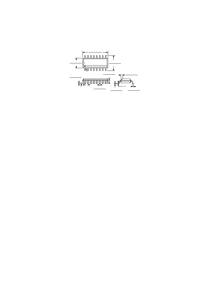
20
C3351810/98
PRINTED IN U.S.A.
ADP3801/ADP3802
REV. 0
OUTLINE DIMENSIONS
Dimensions shown in inches and (mm).
16-Lead Narrow Body (SOIC)
(R-16A)
16
9
8
1
0.3937 (10.00)
0.3859 (9.80)
0.2440 (6.20)
0.2284 (5.80)
0.1574 (4.00)
0.1497 (3.80)
PIN 1
SEATING
PLANE
0.0098 (0.25)
0.0040 (0.10)
0.0192 (0.49)
0.0138 (0.35)
0.0688 (1.75)
0.0532 (1.35)
0.0500
(1.27)
BSC
0.0099 (0.25)
0.0075 (0.19)
0.0500 (1.27)
0.0160 (0.41)
8°
0°
0.0196 (0.50)
0.0099 (0.25)
x 45°