REV. 0
Information furnished by Analog Devices is believed to be accurate and
reliable. However, no responsibility is assumed by Analog Devices for its
use, nor for any infringements of patents or other rights of third parties
which may result from its use. No license is granted by implication or
otherwise under any patent or patent rights of Analog Devices.
a
ADP3301
One Technology Way, P.O. Box 9106, Norwood, MA 02062-9106, U.S.A.
Tel: 617/329-4700
World Wide Web Site: http://www.analog.com
Fax: 617/326-8703
© Analog Devices, Inc., 1997
GENERAL DESCRIPTION
The ADP3301 is a member of the ADP330x family of precision
low dropout anyCAPTM* voltage regulators. The ADP3301
stands out from the conventional LDOs with a novel architec-
ture, an enhanced process and a new package. Its patented
design includes a noninverting wideband driver and a stage that
permits the use of an internal "pole splitting" capacitor to
stabilize the feedback loop with a single output capacitor as
small as 0.47
µ
F. This device is stable with any type of capacitor
regardless of its ESR (Equivalent Serial Resistance) value,
including ceramic types (MLCC) for space restricted applica-
tions. The ADP3301 achieves exceptional accuracy of
±
0.8% at
room temperature and
±
1.4% overall accuracy over tempera-
ture, line and load regulations. The dropout voltage of the
ADP3301 is only 100 mV (typical) at 100 mA.
In addition to the new architecture and process, ADI's new
proprietary thermally enhanced package (Thermal Coastline)
can handle 1 W of power dissipation without external heat sink
or large copper surface on the PC board. This keeps PC board
real estate to a minimum and makes the ADP3301 very
attractive for use in portable equipment.
High Accuracy anyCAPTM*
100 mA Low Dropout Linear Regulator
FEATURES
High Accuracy (Over Line and Load Regulations
at +25 C):
0.8%
Ultralow Dropout Voltage: 100 mV Typical @ 100 mA
Requires Only C
O
= 0.47 F for Stability
anyCAPTM* = Stable with All Types of Capacitors
Current and Thermal Limiting
Low Noise
Dropout Detector
Low Shutdown Current: 1
A
Several Fixed Voltage Options
3.0 V to 12 V Supply Range
20 C to +85 C Ambient Temperature Range
Thermally Enhanced SO-8 Package
Excellent Line and Load Regulations
APPLICATIONS
Cellular Telephones
Notebook, Palmtop Computers
Battery Powered Systems
Portable Instruments
Post Regulator for Switching Supplies
Bar Code Scanners
The ADP3301 operates with a wide input voltage range from
3 V to 12 V and delivers a load current in excess of 100 mA. It
features an error flag that signals when the device is about to
lose regulation or when the short circuit or thermal overload
protection is activated. Other features include shutdown and
optional noise reduction capabilities. The ADP330x anyCAPTM*
LDO family offers a wide range of output voltages and output
current levels from 50 mA to 300 mA:
ADP3300 (50 mA, SOT-23)
ADP3302 (100 mA, Dual Output)
ADP3304 (100 mA, Dual Output with Separate Grounds)
ADP3303 (200 mA)
ADP3306 (300 mA)
ADP3301-5.0
5
4
6
3
NR
OUT
IN
1
2
7
8
ERR
R1
330k
E
OUT
C2
0.47µF
V
OUT
= +5V
ON
OFF
GND
C1
0.47µF
V
IN
Figure 1. Typical Application Circuit
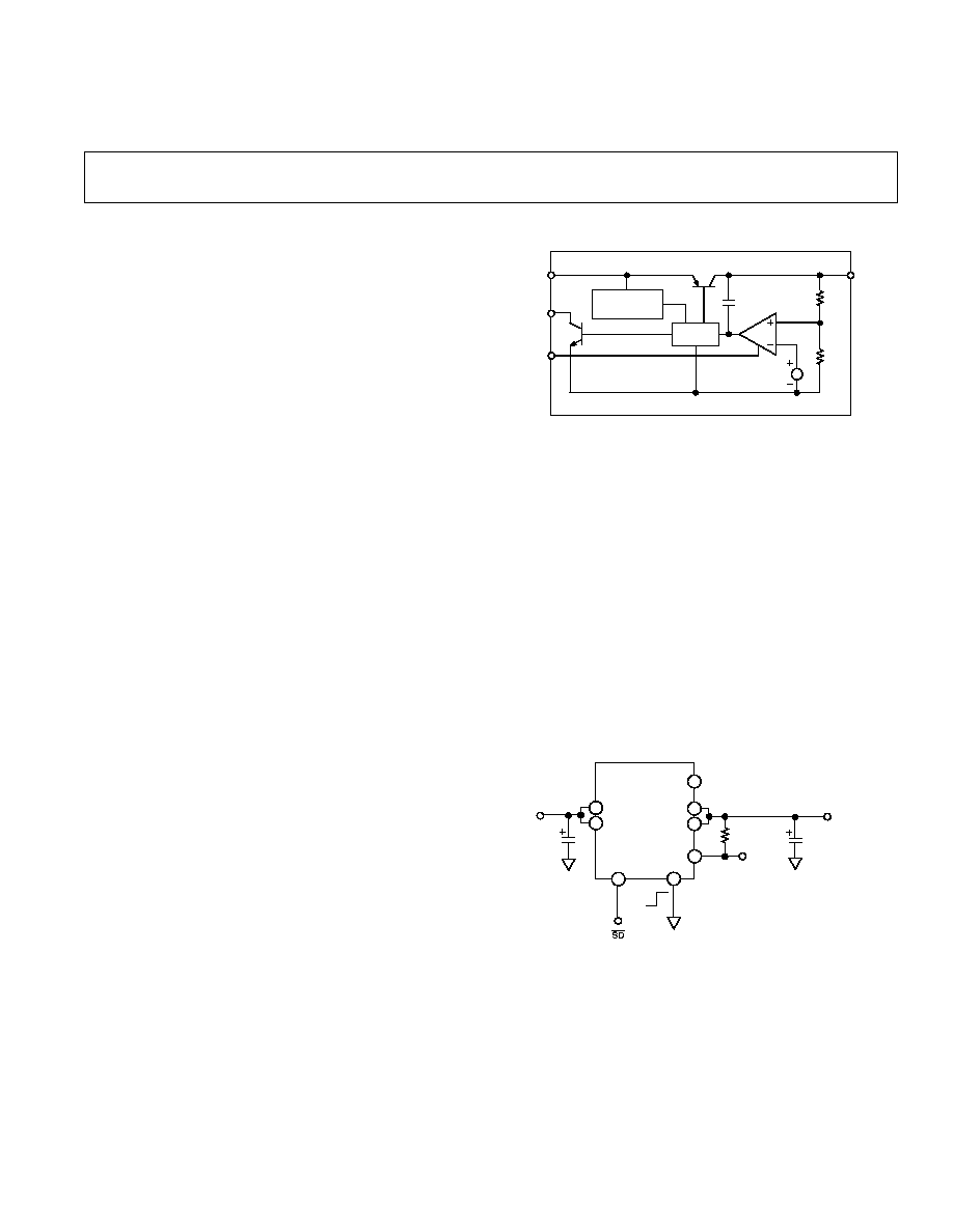
FUNCTIONAL BLOCK DIAGRAM
Q2
THERMAL
PROTECTION
Gm
Q1
CC
BANDGAP
REF
DRIVER
R1
R2
ADP3301
OUT
IN
ERR
SD
GND
*anyCAP is a trademark of Analog Devices Inc.

2
REV. 0
ADP3301xxSPECIFICATIONS
ELECTRICAL CHARACTERISTICS
Parameter
Symbol
Conditions
Min
Typ
Max
Units
OUTPUT VOLTAGE
V
OUT
V
IN
= Nom V
OUT
+0.3 V to 12 V
ACCURACY
I
L
= 0.1 mA to 100 mA
T
A
= +25
°
C
0.8
+0.8
%
V
IN
= Nom V
OUT
+0.3 V to 12 V
I
L
= 0.1 mA to 100 mA
1.4
+1.4
%
LINE REGULATION
V
O
V
IN
= Nom V
OUT
+0.3 V to 12 V
V
IN
T
A
= +25
°
C
0.024
mV/V
LOAD REGULATION
V
O
I
L
= 0.1 mA to 100 mA
I
L
T
A
= +25
°
C
0.014
mV/mA
GROUND CURRENT
I
GND
I
L
= 100 mA
0.85
2
mA
I
L
= 0.1 mA
0.18
0.3
mA
GROUND CURRENT
I
GND
V
IN
= 2.5 V
IN DROPOUT
I
L
= 0.1 mA
0.6
1.2
mA
DROPOUT VOLTAGE
V
DROP
V
OUT
= 98% of V
O
Nominal
I
L
= 100 mA
0.1
0.2
V
I
L
= 10 mA
0.02
0.07
V
I
L
= 1 mA
0.003
0.03
V
SHUTDOWN THRESHOLD
V
THSD
ON
2.0
0.9
V
OFF
0.9
0.3
V
SHUTDOWN PIN
I
SDIN
0 < V
SD
< 5 V
1
µ
A
INPUT
CURRENT
5
V
SD
12 V @ V
IN
= 12 V
22
µ
A
GROUND CURRENT IN
I
Q
V
SD
= 0, V
IN
= 12 V
SHUTDOWN MODE
T
A
= +25
°
C
1
µ
A
V
SD
= 0, V
IN
= 12 V
T
A
= +85
°
C
5
µ
A
OUTPUT CURRENT IN
I
OSD
T
A
= +25
°
C @ V
IN
= 12 V
2
µ
A
SHUTDOWN MODE
T
A
= +85
°
C @ V
IN
= 12 V
4
µ
A
ERROR PIN OUTPUT
LEAKAGE
I
EL
V
EO
= 5 V
13
µ
A
ERROR PIN OUTPUT
"LOW" VOLTAGE
V
EOL
I
SINK
= 400
µ
A
0.13
0.3
V
PEAK LOAD CURRENT
I
LDPK
V
IN
= Nom V
OUT
+ 1 V
200
mA
THERMAL REGULATION
V
O
V
IN
= 12 V, I
L
= 100 mA
V
O
T = 10 ms
0.015
%/W
OUTPUT NOISE
V
NOISE
f = 10 Hz100 kHz
@ 5 V OUTPUT
C
NR
= 0
100
µ
V
rms
C
NR
= 10 nF, C
L
= 10
µ
F
30
µ
V
rms
NOTES
1
Ambient temperature of +85
°
C corresponds to a typical junction temperature of +125
°
C under typical full load test conditions.
Specifications subject to change without notice.
(@ T
A
= 20 C to +85 C, V
IN
= 7 V, C
IN
= 0.47
F, C
OUT
= 0.47 F, unless otherwise noted)
1
ADP3301
3
REV. 0
WARNING!
ESD SENSITIVE DEVICE
CAUTION
ESD (electrostatic discharge) sensitive device. Electrostatic charges as high as 4000 V readily
accumulate on the human body and test equipment and can discharge without detection.
Although the ADP3301 features proprietary ESD protection circuitry, permanent damage may
occur on devices subjected to high energy electrostatic discharges. Therefore, proper ESD
precautions are recommended to avoid performance degradation or loss of functionality.
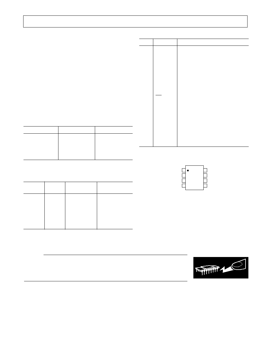
PIN FUNCTION DESCRIPTIONS
Pin
Mnemonic
Function
1 & 2
OUT
Output of the Regulator, fixed 2.7, 3.0,
3.2, 3.3 or 5 volts output voltage. By-
pass to ground with a 0.47
µ
F or larger
capacitor. Pins 1 and 2 must be con-
nected together for proper operation.
3
NR
Noise Reduction Pin. Used for further
reduction of the output noise. (See text
for details.) No connection if not used.
4
GND
Ground Pin.
5
SD
Active Low Shutdown Pin. Connect to
ground to disable the regulator output.
When shutdown is not used, this pin
should be connected to the input pin.
6
ERR
Open Collector Output which goes low
to indicate that the output is about to
go out of regulation.
7 & 8
IN
Regulator Input. Pins 7 and 8 must
be connected together for proper
operation.
PIN CONFIGURATION
1
2
3
4
8
7
6
5
TOP VIEW
(Not to Scale)
PIN FOR 5V DEVICE
OUT
OUT
NR
GND
IN
IN
ERR
SD
ADP3301
ABSOLUTE MAXIMUM RATINGS*
Input Supply Voltage . . . . . . . . . . . . . . . . . . . 0.3 V to +16 V
Shutdown Input Voltage . . . . . . . . . . . . . . . . 0.3 V to +16 V
Error Flag Output Voltage . . . . . . . . . . . . . . . 0.3 V to +16 V
Noise Bypass Pin Voltage . . . . . . . . . . . . . . . . 0.3 V to +5 V
Power Dissipation . . . . . . . . . . . . . . . . . . . Internally Limited
Operating Ambient Temperature Range . . . 55
°
C to +125
°
C
Operating Junction Temperature Range . . . 55
°
C to +125
°
C
JA
. . . . . . . . . . . . . . . . . . . . . . . . . . . . . . . . . . . . . . 96
°
C/W
JC
. . . . . . . . . . . . . . . . . . . . . . . . . . . . . . . . . . . . . . 55
°
C/W
Storage Temperature Range . . . . . . . . . . . . 65
°
C to +150
°
C
Lead Temperature Range (Soldering 10 sec) . . . . . . . . +300
°
C
Vapor Phase (60 sec) . . . . . . . . . . . . . . . . . . . . . . . . +215
°
C
Infrared (15 sec) . . . . . . . . . . . . . . . . . . . . . . . . . . . +220
°
C
*This is a stress rating only; functional operation of the device at these or any other
conditions above those indicated in the operation section of this specification is not
implied. Exposure to absolute maximum rating conditions for extended periods
may affect device reliability.
ORDERING GUIDE
Model
Voltage Output
Package Option*
ADP3301AR-2.7
2.7 V
SO-8
ADP3301AR-3
3.0 V
SO-8
ADP3301AR-3.2
3.2 V
SO-8
ADP3301AR-3.3
3.3 V
SO-8
ADP3301AR-5
5.0 V
SO-8
Contact the factory for the availability of other output voltage options.
*SO = Small Outline.
Other Members of anyCAPTM* Family
1
Output
Package
Model
Current
Option
2
Comments
ADP3300
50 mA
SOT-23
High Accuracy
ADP3302
100 mA
SO-8
Dual Output
ADP3304
100 mA
SO-8
Dual Output with
Separate Grounds
ADP3303
200 mA
SO-8
High Accuracy
ADP3306
300 mA
SO-8,TSSOP-14 High Accuracy,
High Current
NOTES
1
See individual data sheets for detailed ordering information.
2
SO = Small Outline, SOT = Surface Mount, TSSOP = Thin Shrink Small
Outline.

ADP3301
4
REV. 0
Typical Performance Characteristics
INPUT VOLTAGE Volts
5.0003
4.9985
4.9979
5.2
6
7
8
9
10 11 12 13 14
15 16
5.0000
4.9988
4.9982
4.9997
4.9994
4.9991
V
OUT
= 5V
I
L
= 100mA
OUTPUT VOLTAGE Volts
I
L
= 50mA
I
L
= 10mA
I
L
= 0mA
Figure 2. Line Regulation: Output
Voltage vs. Input Voltage
OUTPUT LOAD mA
GROUND CURRENT µA
370
0
10
100
20
30
40 50
60
70 80
90
970
470
270
170
670
570
870
770
I
L
= 0 TO 100mA
Figure 5. Quiescent Current vs. Load
Current
OUTPUT LOAD mA
200
160
0
0
20
200
40
60
80 100 120 140 160 180
120
80
40
INPUT-OUTPUT VOLTAGE mV
Figure 8. Dropout Voltage vs. Output
Current
OUTPUT LOAD mA
OUTPUT VOLTAGE Volts
5.00075
0
20
200
40
60
80 100 120 140 160 180
4.99925
4.99550
4.99850
4.99700
4.99775
4.99625
V
OUT
= 5V
V
IN
= 7V
5.00000
Figure 3. Output Voltage vs. Load
Current Up to 200 mA
TEMPERATURE
°
C
OUTPUT VOLTAGE %
0.2
0.4
45 25
135
5
15
35
75
95
115
55
0.1
0.0
0.1
0.2
0.3
I
L
= 0
Figure 6. Output Voltage Variation %
vs. Temperature
INPUT VOLTAGE Volts
5
0
0
3
0
4
3
2
4
2
1
3
2
1
1
INPUT-OUTPUT VOLTAGE Volts
R
L
= 33
V
OUT
= 3.3V
Figure 9. Power-Up/Power-Down
INPUT VOLTAGE Volts
GROUND CURRENT mA
1.0
0.3
0
1.2
12
2.4 3.6 4.8
6
7.2 8.4 9.6 10.8
0.9
0.4
0.2
0.1
0.6
0.5
0.8
0.7
0
V
OUT
= 5V
I
L
= 0
Figure 4. Quiescent Current vs. Sup-
ply Voltage
TEMPERATURE
°
C
GROUND CURRENT µA
1400
600
0
45 25 15
5
25
45
65
85 105
1200
1000
400
200
800
125
I
L
= 100mA
I
L
= 0
Figure 7. Quiescent Current vs.
Temperature
TIME µs
0
0
100
200
2.0
SD
= V
IN
OR 3V
R
L
= 33
÷
3.3k
C
L
= 0.47µF
V
OUT
= 3.3V
1.0
3.0
4.0
5.0
6.0
7.0
8.0
20
INPUT-OUTPUT VOLTAGE Volts
40 60
80
120 140 160 180
V
IN
V
OUT
Figure 10. Power-Up Overshoot
ADP3301
5
REV. 0
TIME µs
5.02
4.99
0
20
200
40
60
80 100 120 140 160 180
5.01
5.00
7.0
4.98
7.5
Volts
50
, 0.47µF LOAD
V
IN
V
OUT
= 5V
Figure 11. Line Transient Response
TIME µs
Volts 3.300
0
500
100
200
300
400
3.304
3.302
10
3.298
100
mA
C
L
= 10µF
V
OUT
= 3.3V
I(V
OUT
)
Figure 14. Load Transient for 10 mA
to 100 mA Pulse
TIME µs
Volts
4
1
0
5
50
10
15
20 25
30
35 40
45
3
2
0
0
5
V
OUT
V
SD
C = 0.47µF
R = 33
ON 3.3V OUTPUT
V
OUT
= 3.3V
Figure 17. Turn-Off
TIME µs
5.02
4.99
0
40
400
80 120 160 200 240 280 320 360
5.01
5.00
7.0
4.98
7.5
Volts
5k
, 0.47µF LOAD
V
IN
V
OUT
= 5V
Figure 12. Line Transient Response
Volts
TIME sec
3.5
0
0
5
1
2
3
4
0
300
100
400
200
3.3V
mA
V
OUT
I
OUT
Figure 15. Short Circuit Current
FREQUENCY Hz
RIPPLE REJECTION dB
0
100
10
100
10M
1k
10k
100k
1M
10
60
70
80
90
20
30
50
40
a. 0.47µF, R
L
= 33k
b. 0.47µF, R
L
= 33
c. 10µF, R
L
= 33k
d. 10µF, R
L
= 33
b d
a c
b
d
a
c
V
OUT
= 3.3V
Figure 18. Power Supply Ripple
Rejection
TIME µs
mA
5.00
0
1000
200
400
600
800
0.02
5.01
1
4.99
100
Volts
C
L
= 0.47µF
I(V
OUT
)
V
OUT
= 5V
Figure 13. Load Transient for 1 mA
to 100 mA Pulse
TIME µs
4
0
200
40
80
120
160
8
6
0
0
2
5
Volts
C
L
= 0.47µF, R
L
= 5k
C
L
= 10µF, R
L
= 5k
5.0V
V
OUT
= 5V
Figure 16. Turn-On
FREQUENCY Hz
VOLTAGE NOISE SPECTRAL DENSITY µV/ Hz
10
1
0.01
100
1k
100k
10k
0.1
0.47µF BYPASS
PIN 7, 8 TO PIN 3
VOUT = 3.3V, C
L
= 0.47µF,
I
L
= 1mA, C
NR
= 0
VOUT = 5V, C
L
= 0.47µF,
I
L
= 1mA, C
NR
= 0
VOUT = 2.7-5.0V, C
L
= 10µF,
I
L
= 1mA, C
NR
= 10nF
Figure 19. Output Noise Density
ADP3301
6
REV. 0
APPLICATION INFORMATION
anyCAPTM*
The ADP3301 is very easy to use. The only external component
required for stability is a small 0.47
µ
F bypass capacitor on the
output. Unlike the conventional LDO designs, the ADP3301 is
stable with virtually any type of capacitors (anyCAPTM*) indepen-
dent of the capacitor's ESR (Effective Series Resistance) value.
In a typical application, if the shutdown feature is not used, the
shutdown pin (Pin 5) should be tied to the input pin. Pins 7
and 8 must be tied together, as well as Pins 1 and 2, for proper
operation.
Capacitor Selection
Output Capacitors: as with any micropower device, output
transient response is a function of the output capacitance. The
ADP3301 is stable with a wide range of capacitor values, types
and ESR (anyCAPTM*). A capacitor as low as 0.47
µ
F is all that
is needed for stability. However, larger capacitors can be used if
high output current surges are anticipated. The ADP3301 is
stable with extremely low ESR capacitors (ESR
0), such as
multilayer ceramic capacitors (MLCC) or OSCON.
Input Bypass Capacitor: an input bypass capacitor is not
required; however, for applications where the input source is
high impedance or far from the input pins, a bypass capacitor is
recommended. Connecting a 0.47
µ
F capacitor from the input
pins (Pins 7 and 8) to ground reduces the circuit's sensitivity to
PC board layout. If a bigger output capacitor is used, the input
capacitor should be 1
µ
F minimum.
Low ESR capacitors offer better performance on a noisy supply;
however, for less demanding requirements a standard tantalum
or aluminum electrolythic capacitor is adequate.
Noise Reduction
A noise reduction capacitor (C
NR
) can be used to further reduce
the noise by 6 dB10 dB (Figure 20). Low leakage capacitors in
the 10 nF100 nF range provide the best performance. Since
the noise reduction pin (NR) is internally connected to a high
impedance node, any connection to this node should be carefully
done to avoid noise pickup from external sources. The pad
connected to this pin should be as small as possible. Long PC
board traces are not recommended.
IN
OUT
ERR
GND
ADP3301-5.0
NR
+
6
7
8
1
2
3
4
5
ON
OFF
+
SD
C
NR
10nF
C2
10µF
R1
330k
E
OUT
C1
1µF
V
OUT
= 5V
V
IN
Figure 20. Noise Reduction Circuit
Thermal Overload Protection
The ADP3301 is protected against damage due to excessive
power dissipation by its thermal overload protection circuit,
which limits the die temperature to a maximum of 165
°
C.
Under extreme conditions (i.e., high ambient temperature and
high power dissipation) where die temperature starts to rise
above 165
°
C, the output current is reduced until die tempera-
ture has dropped to a safe level. Output current is restored when
the die temperature is reduced.
Current and thermal limit protections are intended to protect
the device against accidental overload conditions. For normal
operation, device power dissipation should be externally limited
so that junction temperatures will not exceed 125
°
C.
Calculating Junction Temperature
Device power dissipation is calculated as follows :
PD = (V
IN
V
OUT
) I
LOAD
+ (V
IN
) I
GND
Where I
LOAD
and I
GND
are load current and ground current, V
IN
and V
OUT
are input and output voltages respectively.
Assuming I
LOAD
= 100 mA, I
GND
= 2 mA, V
IN
= 9 V and
V
OUT
= 5.0 V, device power dissipation is:
PD = (9 V 5 V) 100 mA + (9 V) 2 mA = 418 mW
The proprietary package used in ADP3301 has a thermal
resistance of 96
°
C/W, significantly lower than a standard
8-pin SOIC package at 170
°
C/W.
Junction temperature above ambient temperature will be
approximately equal to :
0.418 W
×
96
°
C/W = 40.1
°
C
To limit the maximum junction temperature to 125
°
C, maxi-
mum ambient temperature must be lower than:
T
A(MAX)
= 125
°
C 40.1
°
C = 84.9
°
C
Printed Circuit Board Layout Consideration
All surface mount packages rely on the traces of the PC board to
conduct heat away from the package.
In standard packages the dominant component of the heat
resistance path is the plastic between the die attach pad and the
individual leads. In typical thermally enhanced packages, one or
more of the leads are fused to the die attach pad, significantly
decreasing this component. However, to make the improvement
meaningful, a significant copper area on the PCB has to be
attached to these fused pins.
The ADP3301's patented thermal coastline lead frame design
uniformly minimizes the value of the dominant portion of the
thermal resistance. It ensures that heat is conducted away by all
pins of the package. This yields a very low 96
°
C/W thermal
resistance for an SO-8 package, without any special board
layout requirements, relying on the normal traces connected to
the leads. The thermal resistance can be decreased by approxi-
mately an additional 10% by attaching a few square cm of
copper area to the V
IN
pin of the ADP3301 package.

ADP3301
7
REV. 0
It is not recommended to use solder mask or silkscreen on the
PCB traces adjacent to the ADP3301's pins since it will increase
the junction to ambient thermal resistance of the package.
Shutdown Mode
Applying a TTL high signal to the shutdown pin, or tying it to
the input pin, will turn the output ON. Pulling the shutdown
pin low, or tying it to ground, will turn the output OFF. In
shutdown mode, quiescent current is reduced to less than 1
µ
A.
Error Flag Dropout Detector
The ADP3301 will maintain its output voltage over a wide
range of load, input voltage and temperature conditions. If, for
example, regulation is lost by reducing the supply voltage below
the combined regulated output and dropout voltages, the ERRor
flag will be activated. The ERR output is an open collector,
which will be driven low.
Once set, the ERRor flag's hysteresis will keep the output low
until a small margin of operating range is restored either by
raising the supply voltage or reducing the load.
APPLICATION CIRCUITS
Crossover Switch
The circuit in Figure 21 shows that two ADP3301s can be used
to form a mixed supply voltage system. The output switches
between two different levels selected by an external digital input.
Output voltages can be any combination of voltages from the
Ordering Guide.
Higher Output Current
The ADP3301 can source up to 100 mA without any heatsink
or pass transistor. If higher current is needed, an appropriate
pass transistor can be used, as in Figure 22, to increase the
output current to 1 A.
Step-Up/Step-Down Post Regulator
The circuit in Figure 23 provides a high precision, low dropout
regulated output voltage. It significantly reduces the ripple from
a switching regulator. The ADP3000 used in this circuit is a
switching regulator in the step-up configuration.
D1
1N5817
C2
100µF
10V
L1
6.8µH
R1
120
R2
19.6k
1%
R3
10k
1%
ADP3301-3.3
IN
OUT
GND
C3
2.2µF
3.3V @ 100mA
C1
100µF
10V
ADP3000-ADJ
I
LIM
V
IN
SW1
GND
SW2
FB
V
IN
= 2.5V TO 3.5V
Figure 23. Step-Up/Step-Down Post Regulator
V
OUT
= 5V/3.3V
V
IN
= 5.5V TO 12V
OUTPUT SELECT
5V
0V
C2
0.47µF
IN
OUT
GND
SD
ADP3301-5.0
+
+
IN
OUT
GND
SD
ADP3301-3.3
C1
1.0µF
Figure 21. Crossover Switch
V
IN
= 6V TO 8V
V
OUT
= 5V @ 1A
MJE253*
C2
10µF
C1
47µF
R1
50
*AAVID531002 HEAT SINK IS USED
IN
OUT
ERR
GND
SD
ADP3301-5
Figure 22. High Output Current Linear Regulator

ADP3301
8
REV. 0
OUTLINE DIMENSIONS
Dimensions shown in inches and (mm).
C2985-12-2/97
PRINTED IN U.S.A.
8-Pin Small Outline Package
(SO-8)
0.1968 (5.00)
0.1890 (4.80)
8
5
4
1
0.2440 (6.20)
0.2284 (5.80)
PIN 1
0.1574 (4.00)
0.1497 (3.80)
0.0688 (1.75)
0.0532 (1.35)
SEATING
PLANE
0.0098 (0.25)
0.0040 (0.10)
0.0192 (0.49)
0.0138 (0.35)
0.0500
(1.27)
BSC
0.0098 (0.25)
0.0075 (0.19)
0.0500 (1.27)
0.0160 (0.41)
8
°
0
°
0.0196 (0.50)
0.0099 (0.25)
x 45
°