Äîêóìåíòàöèÿ è îïèñàíèÿ www.docs.chipfind.ru
3.3 V Slew Rate Limited,
Half Duplex RS-485/RS-422 Transceiver
ADM3493
Rev. 0
Information furnished by Analog Devices is believed to be accurate and reliable. However, no
responsibility is assumed by Analog Devices for its use, nor for any infringements of patents or other
rights of third parties that may result from its use. Specifications subject to change without notice. No
license is granted by implication or otherwise under any patent or patent rights of Analog Devices.
Trademarks and registered trademarks are the property of their respective owners.
One Technology Way, P.O. Box 9106, Norwood, MA 02062-9106, U.S.A.
Tel: 781.329.4700
www.analog.com
Fax: 781.461.3113
©2005 Analog Devices, Inc. All rights reserved.
FEATURES
Operates with 3.3 V supply
Interoperable with 5 V logic
EIA RS-422 and RS-485 compliant over full CM range
Data rate: 250 kbps
Half duplex transceiver
Reduced slew rates for low EMI
2 nA supply current in shutdown mode
Up to 256 transceivers on a bus
-7 V to +12 V bus common-mode range
Specified over -40°C to +85°C temperature range
8 ns skew
Available in 8-lead SOIC
APPLICATIONS
Low power RS-485 applications
EMI sensitive systems
DTE-DCE interfaces
Industrial control
Packet switching
Local area networks
Level translators
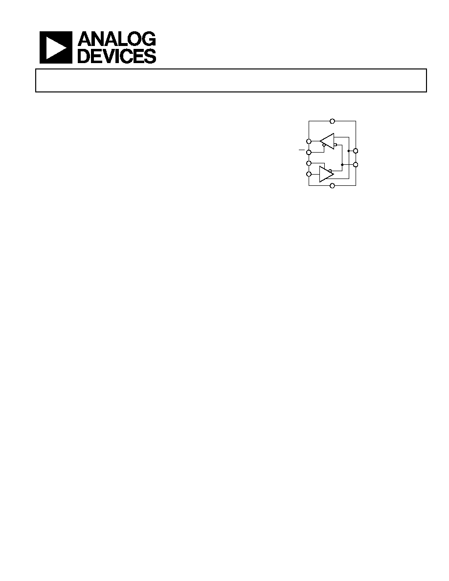
FUNCTIONAL BLOCK DIAGRAM
R
D
RO
V
CC
RE
DI
DE
ADM3493
A
GND
B
05
71
5-
00
1
Figure 1.
GENERAL DESCRIPTION
The ADM3493 is a low power, differential line transceiver
designed to operate using a single 3.3 V power supply. Low
power consumption, coupled with a shutdown mode, makes it
ideal for power-sensitive applications. The ADM3493 is suitable
for communication on multipoint bus transmission lines.
The device contains one driver and one receiver. Designed for
half-duplex communication, the ADM3493 features a slew rate
limited driver that minimizes EMI and reduces reflections
caused by improperly terminated cables, allowing error-free
data transmission at data rates up to 250 kbps.
The receiver input impedance is 96 k, allowing up to 256
transceivers to be connected on the bus. A thermal shutdown
circuit prevents excessive power dissipation caused by bus
contention or by output shorting. If a significant temperature
increase is detected in the internal driver circuitry during fault
conditions then the thermal shutdown circuit forces the driver
output into a high impedance state. The receiver contains a fail-
safe feature that results in a logic high output state, if the inputs
are unconnected (floating).
The ADM3493 is fully specified over the commercial and
industrial temperature ranges and is available in an 8-lead SOIC.

ADM3493
Rev. 0 | Page 2 of 12
TABLE OF CONTENTS
Features .............................................................................................. 1
Applications....................................................................................... 1
Functional Block Diagram .............................................................. 1
General Description ......................................................................... 1
Revision History ............................................................................... 2
Specifications..................................................................................... 3
Timing Specifications .................................................................. 4
Absolute Maximum Ratings............................................................ 5
ESD Caution.................................................................................. 5
Pin Configurations and Function Descriptions ........................... 6
Test Circuits....................................................................................... 7
Switching Characteristics .................................................................8
Typical Performance Characteristics ..............................................9
Circuit Description......................................................................... 11
Reduced EMI and Reflections .................................................. 11
Low Power Shutdown Mode..................................................... 11
Driver Output Protection.......................................................... 11
Propagation Delay ...................................................................... 11
Typical Applications................................................................... 11
Outline Dimensions ....................................................................... 12
Ordering Guide .......................................................................... 12
REVISION HISTORY
10/05--Rev. 0: Initial Version
ADM3493
Rev. 0 | Page 3 of 12
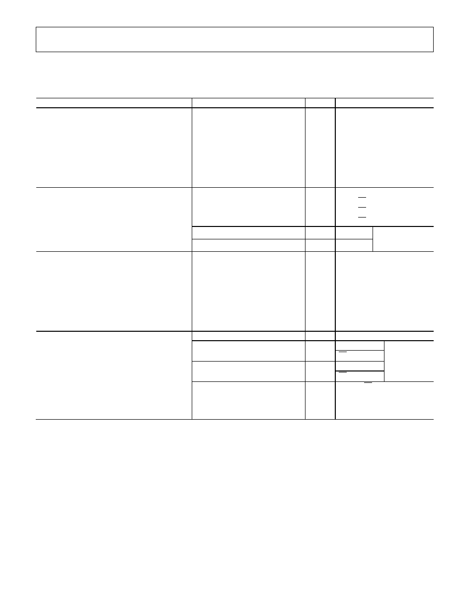
SPECIFICATIONS
V
CC
= 3.3 V ±0.3 V, T
A
= T
MIN
to T
MAX
, unless otherwise noted.
Table 1.
Parameter Min
Typ
Max
Units
Test
Conditions/Comments
DRIVER
Differential Output Voltage, V
OD
2.0
V
R
L
= 100 (RS-422), V
cc
= 3.3 V
±5% (see Figure 3)
1.5
V
R
L
= 54 (RS-485) (see Figure 3)
1.5
V
R
L
= 60
(RS-485), V
cc
= 3.3 V
(see Figure 4)
|V
OD
| for Complementary Output States
1
0.2
V
R
L
= 54 or 100 (see Figure 3)
Common-Mode Output Voltage, V
OC
3
V
R
L
= 54 or 100 (see Figure 3)
|V
OC
| for Common-Mode Output Voltage
1
0.2
V
R
L
= 54 or 100 (see Figure 3)
DRIVER INPUT LOGIC
CMOS Input Logic Threshold Low, V
IH
0.8
V
DE, DI, RE
CMOS Input Logic Threshold High, V
IL
2.0
V
DE, DI, RE
CMOS Logic Input Current, I
N1
±2
A
DE, DI, RE
60
A
V
IN
= 12 V
Input Current (A, B), I
N2
-60
A
V
IN
= -7 V
DE = 0 V
V
CC
= 0 V or 3.6 V
RECEIVER
Differential Input Threshold Voltage, V
TH
-0.2
0.2
V
-7V
<
V
CM
< + 12 V
Input Hysteresis,
V
TH
50
mV
V
CM
= 0 V
CMOS Output Voltage High, V
OH
V
cc
0.4
V
I
OUT
= -1.5 mA, V
ID
= 200 mV
(see Figure 5)
CMOS Output Voltage Low, V
OL
0.4
V
I
OUT
= 2.5mA, V
ID
= 200mV
(see Figure 5)
Three-State Output Leakage Current, I
OZR
±1
A
V
cc
= 3.6 V, 0 V
V
OUT
V
cc
Input Resistance, R
IN
96
k
-7 V < V
CM
< + 12 V
POWER SUPPLY CURRENT
DE = V
CC
1.1
2.2
mA
RE = 0 V or V
CC
DE = V
CC
Supply Current
0.95
1.9
mA
RE = 0 V
No load,
DI = 0 V or V
CC
Supply Current in Shutdown Mode, I
SHDN
0.002
1
A
DE = 0 V, RE = V
CC
, DI = V
CC
or 0 V
-250
mA
V
OUT
= -7 V
Driver Short-Circuit Output Current, I
OSD
250
mA
V
OUT
= 12 V
Receiver Short-Circuit Output Current, I
OSR
±8
±60
mA
0
V
<
V
RO
< V
CC
1
V
OD
and
V
OC
are the changes in V
OD
and V
OC
, respectively, when DI input changes state.

ADM3493
Rev. 0 | Page 4 of 12
TIMING SPECIFICATIONS
V
CC
= 3.3 V, T
A
= 25°C, unless otherwise noted.
Table 2.
Parameter Min
Typ
Max
Units
Test
Conditions/Comments
DRIVER
Differential Output Delay, t
DD
600
900
1400
ns
R
L
= 60
(see Figure 6 and Figure 12)
Differential Output Transition Time, t
TD
400 700
1200 ns
R
L
= 60
(see Figure 6 and Figure 12)
Propagation Delay, Low-to-High Level, t
PLH
700
1000
1500
ns
R
L
= 27
(see Figure 7 and Figure 13)
Propagation Delay, High-to-Low Level, t
PHL
700
1000
1500
ns
R
L
= 27
(see Figure 7 and Figure 13)
|t
PLH
t
PHL
| Propagation Delay Skew
1
, t
PDS
100
ns R
L
= 27 (see Figure 7 and Figure 13)
DRIVER OUTPUT ENABLE/DISABLE TIMES
Output Enable Time to Low Level, t
PZL
900
1300
ns
R
L
= 110
(see Figure 9 and Figure 15)
Output Enable Time to High Level, t
PZH
600
800
ns
R
L
= 110
(see Figure 8 and Figure 14)
Output Disable Time from High Level, t
PHZ
50 80
ns
R
L
= 110
(see Figure 8 and Figure 14)
Output Disable Time from Low Level, t
PLZ
50 80
ns
R
L
= 110
(see Figure 9 and Figure 15)
Output Enable Time from Shutdown to
Low Level, t
PSL
1.9
2.7
s
R
L
= 110
(see Figure 9 and Figure 15)
Output Enable Time from Shutdown to
High Level, t
PSH
2.2
3.0
s
R
L
= 110
(see Figure 8 and Figure 14)
RECEIVER
Time to Shutdown
2
, t
SHDN
80
190
300
ns
Propagation Delay, Low-to-High Level, t
RPLH
25
75
180
ns
V
ID
= 0 V to 3.0 V, C
L
= 15 pF (see Figure 10
and Figure 16)
Propagation Delay, High-to-Low Level, t
RPHL
25
75
180
ns
V
ID
= 0 V to 3.0 V, C
L
= 15 pF (see Figure 10
and Figure 16)
|t
PLH
t
PHL
| Propagation Delay Skew, t
RPDS
50
ns V
ID
= 0 V to 3.0 V, C
L
= 15 pF (see Figure 10
and Figure 16)
RECEIVER OUTPUT ENABLE/DISABLE TIMES
Output Enable Time to Low Level, t
PRZL
25
50 ns
C
L
= 15 pF (see Figure 11 and Figure 17)
Output Enable Time to High Level, t
PRZH
25
50
ns C
L
= 15 pF (see Figure 11 and Figure 17)
Output Disable Time from High Level, t
PRHZ
25
45
ns
C
L
= 15 pF (see Figure 11 and Figure 17)
Output Disable Time from Low Level, t
PRLZ
25
45
ns C
L
= 15 pF (see Figure 11 and Figure 17)
Output Enable Time from Shutdown to
Low Level, t
PRSL
720
1400
ns
C
L
= 15 pF (see Figure 11 and Figure 17)
Output Enable Time from Shutdown to
High Level, t
PRSH
720
1400
ns
C
L
= 15 pF (see Figure 11 and Figure 17)
1
Measured on |t
PLH
(A) - t
PHL
(A)| and |t
PLH
(B) - t
PHL
(B)|.
2
The transceivers are put into shutdown by bringing RE high and DE low. If the inputs are in this state for less than 80 ns, the parts are guaranteed not to enter
shutdown. If the inputs are in this state for at least 300 ns, the parts are guaranteed to enter shutdown.
ADM3493
Rev. 0 | Page 5 of 12
ABSOLUTE MAXIMUM RATINGS
T
A
= 25°C, unless otherwise noted.
Table 3.
Parameter
Rating
V
CC
to GND
7 V
Digital I/O Voltage (DE, RE, DI)
-0.3 V to V
CC
+ 0.3 V
Digital I/O Voltage (R
OUT
) V
CC
- 0.5 V to V
CC
+ 0.5 V
Driver Output/Receiver Input Voltage
-7.5 V to +12.5 V
Operating Temperature Range
-40°C to +85°C
Storage Temperature Range
-65°C to +125°C
JA
Thermal Impedance
8-Lead SOIC
121°C/W
Lead Temperature
Soldering (10 seconds)
300°C
Vapor Phase (60 seconds)
215°C
Infrared (15 seconds)
220°C
Stresses above those listed under Absolute Maximum Ratings
may cause permanent damage to the device. This is a stress
rating only; functional operation of the device at these or any
other conditions above those indicated in the operational
section of this specification is not implied. Exposure to absolute
maximum rating conditions for extended periods may affect
device reliability.
ESD CAUTION
ESD (electrostatic discharge) sensitive device. Electrostatic charges as high as 4000 V readily accumulate on
the human body and test equipment and can discharge without detection. Although this product features
proprietary ESD protection circuitry, permanent damage may occur on devices subjected to high energy
electrostatic discharges. Therefore, proper ESD precautions are recommended to avoid performance
degradation or loss of functionality.
ADM3493
Rev. 0 | Page 6 of 12
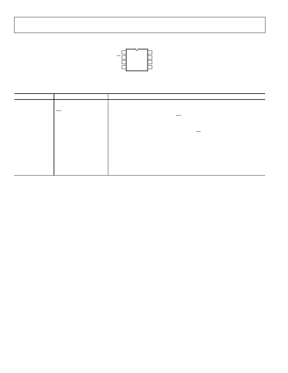
PIN CONFIGURATION AND FUNCTION DESCRIPTIONS
RO
1
RE
2
DE
3
DI
4
V
CC
8
B
7
A
6
GND
5
ADM3493
TOP VIEW
(Not to Scale)
05
71
5-
00
2
Figure 2. Pin Configuration
Table 4. . Pin Function Descriptions
Pin No.
Mnemonic
Description
1 RO
Receiver Output. When enabled, if A > B by 200 mV, then RO = high.
If A < B by 200 mV, then RO = low.
2
RE
Receiver Output Enable. A low level enables the receiver output, RO. A high level
places it in a high impedance state. If RE is high and DE is low, the device enters a low
power shutdown mode.
3 DE
Driver Output Enable. A high level enables the driver differential Outputs A and B.
A low level places it in a high impedance state. If RE is high and DE is low, the device
enters a low power shutdown mode.
4 DI
Driver Input. When the driver is enabled, a logic low on DI forces A low and B high
while a logic high on DI forces A high and B low.
5 GND
Ground.
6
A
Noninverting Receiver Input A and Noninverting Driver Output A.
7
B
Inverted Receiver Input B and Inverted Driver Output B.
8 V
CC
Power Supply, 3.3 V ± 0.3 V.
ADM3493
Rev. 0 | Page 7 of 12
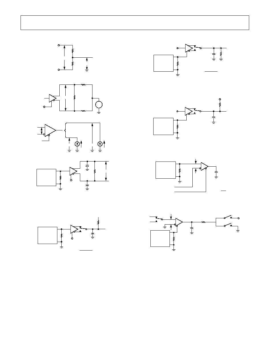
TEST CIRCUITS
R
L
/2
R
L
/2
V
OC
A
B
V
OD
05
71
5-
0
03
Figure 3. Driver V
OD
and V
OC
V
CM
=
7V TO +12V
V
CC
R
L
375
375
V
OD
D
05
71
5-
00
4
Figure 4. Driver V
OD
with Varying Common-Mode Voltage
0
57
15
-
00
5
I
OH
()
I
OL
(+)
V
OH
V
OL
R
0
V
ID
Figure 5. Receiver V
OH
and V
OL
D
GENERATOR
1
V
CC
50
C
L
R
L
=
60
C
L
= 15pF
2
05
71
5-
00
6
OUT
1
PPR = 250kHz, 50% DUTY CYCLE,
t
R
6.0ns, Z
O
= 50.
2
C
L
INCLUDES PROBE AND STRAY CAPACITANCE.
Figure 6. Driver Differential Output Delay and Transition Times
D
V
OM
R
L
= 27
OUT
C
L
= 15pF
2
GENERATOR
1
V
CC
50
S1
V
OM
=
V
OH
+ V
OL
2
1.5V
05
71
5-
00
7
1
PPR = 250kHz, 50% DUTY CYCLE,
t
R
6.0ns, Z
O
= 50.
2
C
L
INCLUDES PROBE AND STRAY CAPACITANCE.
Figure 7. Driver Propagation Delays
D
OUT
C
L
= 50pF
2
GENERATOR
1
50
S1
V
OM
=
V
OH
+ V
OL
2
1.5V
R
L
= 110
0V OR 3V
05
71
5-
00
8
1
PPR = 250kHz, 50% DUTY CYCLE,
t
R
6.0ns, Z
O
= 50.
2
C
L
INCLUDES PROBE AND STRAY CAPACITANCE.
Figure 8. Driver Enable and Disable Times (t
PZH
, t
PSH
, t
PHZ
)
D
OUT
C
L
= 50pF
2
GENERATOR
1
50
S1
0V OR 3V
V
CC
R
L
= 110
05
71
5-
0
09
1
PPR = 250kHz, 50% DUTY CYCLE,
t
R
6.0ns, Z
O
= 50.
2
C
L
INCLUDES PROBE AND STRAY CAPACITANCE.
Figure 9. Driver Enable and Disable Times (t
PZL
, t
PSL
, t
PLZ
)
0
571
5-
0
10
GENERATOR
1
50
C
L
= 15pF
2
R
1.5V
0
V
OM
=
V
CC
2
OUT
V
ID
1
PPR = 250kHz, 50% DUTY CYCLE,
t
R
6.0ns, Z
O
= 50.
2
C
L
INCLUDES PROBE AND STRAY CAPACITANCE.
Figure 10. Receiver Propagation Delay
R
GENERATOR
1
50
C
L
2
S3
S1
S2
V
CC
+1.5V
1.5V
V
ID
1k
0
571
5-
0
1
1
1
PPR = 250kHz, 50% DUTY CYCLE,
t
R
6.0ns, Z
O
= 50.
2
C
L
INCLUDES PROBE AND STRAY CAPACITANCE.
Figure 11. Receiver Enable and Disable Times
ADM3493
Rev. 0 | Page 8 of 12
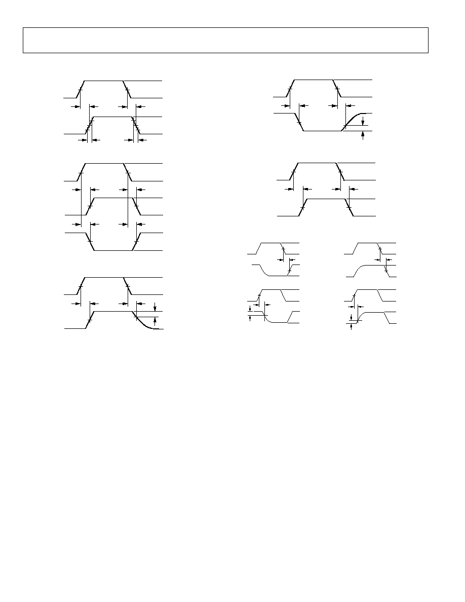
SWITCHING CHARACTERISTICS
IN
OUT
1.5V
1.5V
+3V
0
+2V
2V
t
DD
t
DD
t
TD
t
TD
50%
50%
10%
10%
90%
90%
05
71
5-
0
12
Figure 12. Driver Differential Output Delay and Transition Times
3V
0V
V
OH
V
OL
V
OH
V
OL
V
OM
V
OM
V
OM
V
OM
IN
A
OUT
B
OUT
1.5V
1.5V
t
PLH
t
PHL
t
PHL
t
PLH
05
71
5-
01
3
Figure 13. Driver Propagation Delays
0
V
OH
0
3V
1.5V
1.5V
0.25V
IN
OUT
V
OM
t
PZH
t
PHZ
05
71
5
-
01
4
Figure 14. Driver Enable and Disable Times (t
PZH
, t
PSH
, t
PHZ
)
V
OL
V
CC
0
3V
0.25V
IN
OUT
1.5V
1.5V
t
PSL
t
PLZ
V
OM
05
71
5-
0
15
Figure 15. Driver Enable and Disable Times (t
PZL
, t
PSL
, t
PLZ
)
05
71
5-
0
16
3V
0
V
CC
0
IN
OUT
V
OM
V
OM
1.5V
1.5V
t
RPHL
t
RPLH
Figure 16. Receiver Propagation Delay
+3V
0
V
OH
0
S1 OPEN
S2 CLOSED
S3 = +1.5V
S1 CLOSED
S2 OPEN
S3 = 1.5V
S1 OPEN
S2 CLOSED
S3 = +1.5V
S1 CLOSED
S2 OPEN
S3 = 1.5V
+3V
0
V
CC
V
OL
+3V
0
V
CC
V
OL
+3V
0
V
OH
0
+1.5V
+1.5V
+1.5V
IN
OUT
IN
OUT
IN
OUT
IN
OUT
t
PRZL
t
PRSL
t
PRLZ
t
PRHZ
+0.25V
+0.25V
+1.5V
+1.5V
+1.5V
t
PRZH
t
PRSH
0
57
15-
01
7
Figure 17. Receiver Enable and Disable Times
ADM3493
Rev. 0 | Page 9 of 12
05
71
5-
0
18
OUTPUT VOLTAGE (V)
O
U
T
P
U
T
CUR
RE
NT
(
m
A)
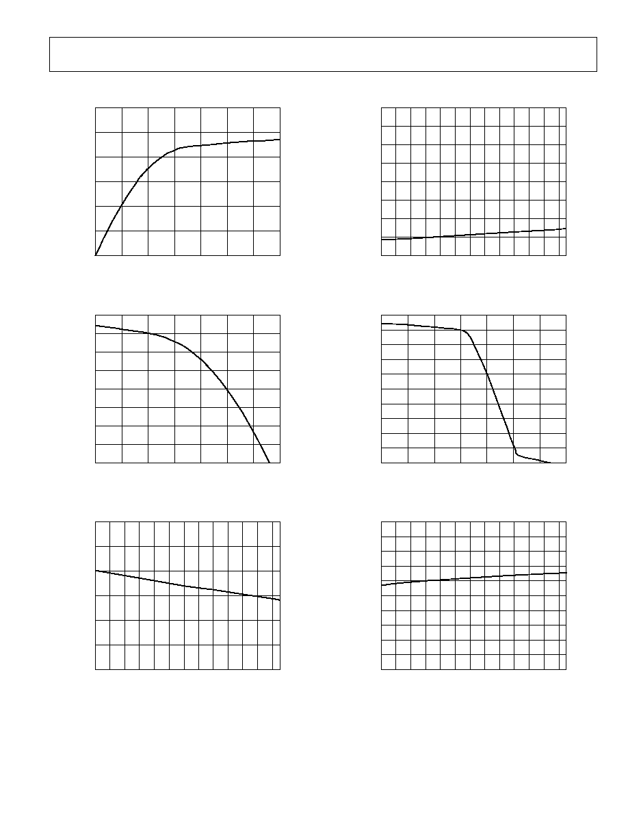
TYPICAL PERFORMANCE CHARACTERISTICS
30
0
0
3.5
0.8
0
40
05
71
5-
0
21
TEMPERATURE (°C)
O
UT
P
UT
V
O
L
T
AG
E
(
V
)
0.7
0.6
0.5
0.4
0.3
0.2
0.1
25
20
15
10
5
0.5
1.0
1.5
2.0
2.5
3.0
30 20 10
0
10
20
30
40
50
60
70
80
Figure 18. Output Current vs. Receiver Output Low Voltage
16
0
0
3.5
05
71
5-
0
19
OUTPUT VOLTAGE (V)
O
U
T
P
U
T
CUR
RE
NT
(
m
A)
14
12
10
8
6
4
2
0.5
1.0
1.5
2.0
2.5
3.0
Figure 19. Output Current vs. Receiver Output High Voltage
3.30
3.00
40
05
71
5-
0
20
TEMPERATURE (°C)
O
UT
P
UT
V
O
L
T
AG
E
(
V
)
3.25
3.20
3.15
3.10
3.05
30 20 10
0
10
20
30
40
50
60
70
80
Figure 20. Receiver Output High Voltage vs. Temperature, I
O
= 1.5 mA
Figure 21. Receiver Output Low Voltage vs. Temperature, I
O
= 2.5 mA
100
0
0
3.5
05
71
5-
0
22
OUTPUT VOLTAGE (V)
O
U
T
P
U
T
CUR
RE
NT
(
m
A)
90
80
70
60
50
40
30
20
10
0.5
1.0
1.5
2.0
2.5
3.0
Figure 22. Driver Output Current vs. Differential Output Voltage
2.6
1.6
40
05
71
5-
0
23
TEMPERATURE (°C)
O
UT
P
UT
V
O
L
T
AG
E
(
V
)
30 20 10
0
10
20
30
40
50
60
70
80
2.5
2.4
2.3
2.2
2.1
2.0
1.9
1.8
1.7
Figure 23. Driver Differential Output Voltage vs. Temperature, RI = 54
ADM3493
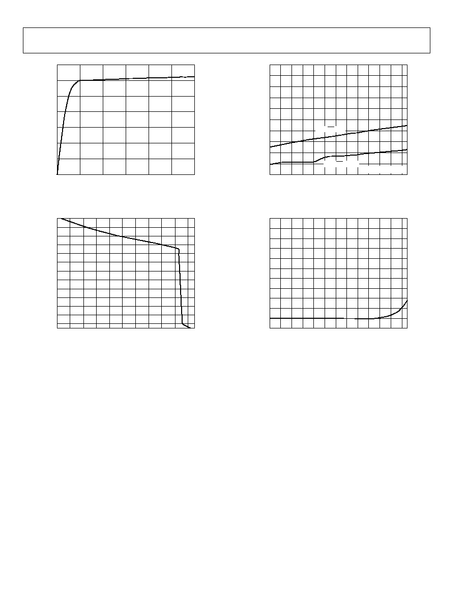
Rev. 0 | Page 10 of 12
05
71
5-
0
24
OUTPUT VOLTAGE (V)
O
U
T
P
U
T
CUR
RE
NT
(
m
A)
140
0
0
12
1.2
0.2
40
05
71
5-
0
26
TEMPERATURE (°C)
S
UP
P
L
Y
C
URRE
N
T
(
m
A)
1.1
120
100
80
60
40
20
2
4
6
8
10
1.0
0.9
0.8
0.7
Figure 24. Output Current vs. Driver Output Low Voltage
125
5
7
3
05
71
5-
0
25
OUTPUT VOLTAGE (V)
O
U
T
P
U
T
CUR
RE
NT
(
m
A)
115
105
95
85
75
65
55
45
35
25
15
6
5
4
3
2
1
0
1
2
Figure 25. Output Current vs. Driver Output High Voltage
30 20 10
0
10
20
30
40
50
60
70
80
0.6
0.5
0.4
DE = RE = X*
0.3
DE = RE = GND
*X = DON'T CARE
Figure 26. Supply Current vs. Temperature
40
05
71
5-
0
27
TEMPERATURE (°C)
S
HUT
DO
W
N CUR
RE
NT
(
n
A)
30 20 10
0
10
20
30
40
50
60
70
80
80
70
60
50
40
30
20
10
0
10
100
90
Figure 27. Shutdown Current vs. Temperature, V
CC
= 3.3 V
ADM3493
Rev. 0 | Page 11 of 12
CIRCUIT DESCRIPTION
The ADM3493 is a low power transceiver for RS-485 and
RS-422 communications. The ADM3493 can transmit and
receive at data rates up to 250 kbps in a half duplex
configuration. Driver Enable (DE) and Receiver Enable (RE)
pins are included when disabled; the driver and receiver
outputs are high impedance.
Table 5. Transmitting Truth Table
Transmitting Inputs
Transmitting
Outputs
RE
DE DI B A
Mode
X
1
1 1 0 1
Normal
X
1
1 0 1 0
Normal
0 0 X
1
High-Z
2
High-Z
2
Normal
1 0 X
1
High-Z
2
High-Z
2
Shutdown
1
X = Don't care.
2
High-Z = High Impedance.
Table 6. Receiving Truth Table
Receiving Inputs
Receiving
Outputs
RE
DE
A - B
RO
Mode
0 0 +0.2
V 1 Normal
0 0 -0.2
V 0 Normal
0 0
Inputs
Open 1 Normal
1 0
X
1
High-Z
2
Shutdown
1
X = Don't care.
2
High-Z = High Impedance
REDUCED EMI AND REFLECTIONS
The ADM3493 is a slew rate limited transceiver, minimizing
EMI and reducing reflections caused by improperly terminated
cables.
LOW POWER SHUTDOWN MODE
A low power shutdown mode is initiated by bringing both RE
high and DE low. The ADM3493 does not shut down unless
both the driver and receiver are disabled (high impedance). In
shutdown, the ADM3493 typically draws only 2 nA of supply
current. For the ADM3493, the t
PSH
and t
PSL
enable times assume
the part was in the low power shutdown mode; the t
PZH
and t
PZL
enable times assume the receiver or driver was disabled, but the
part was not shut down.
DRIVER OUTPUT PROTECTION
Two methods are implemented to prevent excessive output
current and power dissipation caused by faults or by bus
contention. Current limit protection on the output stage
provides immediate protection against short circuits over the
whole common-mode voltage range (see Typical Performance
Characteristics). In addition, a thermal shutdown circuit forces
the driver outputs into a high impedance state if the die
temperature rises excessively.
PROPAGATION DELAY
Skew time is simply the difference between the low-to-high and
high-to-low propagation delay. Small driver/receiver skew times
help maintain a symmetrical mark-space ratio (50% duty cycle).
The receiver skew time, |t
PRLH
- t
PRHL
|, is 20 ns for the ADM3493.
The driver skew time is typically under 100 ns.
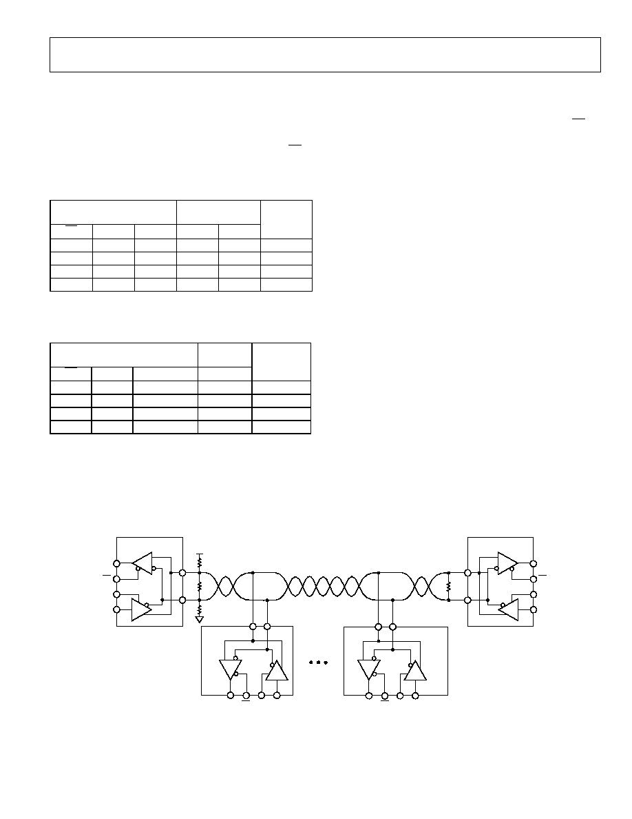
TYPICAL APPLICATIONS
The ADM3493 transceiver is designed for bidirectional data
communications on multipoint bus transmission lines. Figure
22 shows a typical network application's circuits. To minimize
reflections, the line should be terminated at both ends in its
characteristic impedance, and stub lengths off the main line
should be kept as short as possible. The slew rate limited
ADM3493 is tolerant of imperfect termination.
B
A
R
D
RO
RE
DI
DE
ADM3493
ADM3493
ADM3493
ADM3493
B
A
R
D
RO
RE
DI
DE
B
A
R
D
RO RE
DI
DE
B
A
R
D
RO
RE
DI
DE
05
71
5
-
02
8
MAXIMUM NUMBER OF TRANSCEIVERS ON BUS = 256
R
T
R
T
NOTES
1. R
T
IS EQUAL TO THE CHARACTERISTIC IMPEDANCE OF THE CABLE.
V
CC
R1
R2
Figure 28. ADM3493 Typical Half Duplex RS-485 Network
ADM3493
Rev. 0 | Page 12 of 12
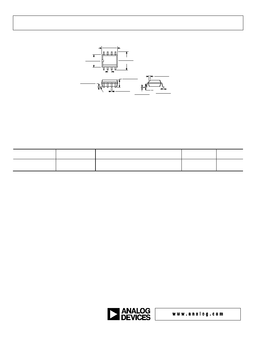
OUTLINE DIMENSIONS
0.25 (0.0098)
0.17 (0.0067)
1.27 (0.0500)
0.40 (0.0157)
0.50 (0.0196)
0.25 (0.0099)
× 45°
8°
0°
1.75 (0.0688)
1.35 (0.0532)
SEATING
PLANE
0.25 (0.0098)
0.10 (0.0040)
4
1
8
5
5.00 (0.1968)
4.80 (0.1890)
4.00 (0.1574)
3.80 (0.1497)
1.27 (0.0500)
BSC
6.20 (0.2440)
5.80 (0.2284)
0.51 (0.0201)
0.31 (0.0122)
COPLANARITY
0.10
CONTROLLING DIMENSIONS ARE IN MILLIMETERS; INCH DIMENSIONS
(IN PARENTHESES) ARE ROUNDED-OFF MILLIMETER EQUIVALENTS FOR
REFERENCE ONLY AND ARE NOT APPROPRIATE FOR USE IN DESIGN
COMPLIANT TO JEDEC STANDARDS MS-012-AA
Figure 29. 8-Lead Standard Small Outline Package [SOIC_N]
Narrow Body
(R-8)
Dimensions shown in millimeters and (inches)
ORDERING GUIDE
Model
Temperature Range
Package Description
Package Options
Ordering
Quantity
ADM3493ARZ
1
-40°C to +85°C
8-Lead Standard Small Outline Package [SOIC_N]
R-8
ADM3493ARZ-REEL7
1
-40°C to +85°C
8-Lead Standard Small Outline Package [SOIC_N]
R-8
1,000
1
Z = Pb-free part.
© 2005 Analog Devices, Inc. All rights reserved. Trademarks and
registered trademarks are the property of their respective owners.
D05715-0-10/05(0)
Document Outline
- þÿ
- þÿ
- FUNCTIONAL BLOCK DIAGRAM
- þÿ
- þÿ
- þÿ