ADM1203 Simple Tracker with Circuit Breaker Preliminary Data Sheet (Rev. PrD)
Simple Tracker
TM
with
Circuit Breaker
Preliminary Technical Data
ADM1203
FEATURES
Enables Power Supply Tracking of multiple Supplies
Monitors Current on Supply being Tracked
Up/Down Tracking limits Supply Differences to ~100mV
Capacitor Adjustable Slew Rate
On Board Charge Pump Fully enhances FET
Ability to Track Down Supplies (ADM1203-1/3)
Emergency Shutdown Feature (ADM1203-2/4)
Auto retry after Current Fault (ADM1203-1/2)
Latch off after Current Fault (ADM1203-3/4)
Packaged in tiny 8-Lead TSOT Package
APPLICATIONS
Multi-Voltage Supply Rail Tracker
Telecoms and Datacom s Systems
Multi voltage Network Processors , FPGAs, ASICs, DSPs
PC/Server Applications
GENERAL DESCRIPTION
The ADM1203 is a cascadable Simple Tracker
TM
device which
ensures that voltage rails track within ~100mV of each other in
multi supply systems. Any number of these devices can be
cascaded to form a multi supply tracking solution.
The ADM1203 requires 2.7V to 16.5V on its Vcc pin to operate.
An on-board charge pump generates a high voltage GATE drive
to fully enhance FETs in the power path.
The Slew Rate of the ramp is adjustable via an external capacitor
on the C
SLEW
pin and can be programmed from 100V/s to
1000V/s. When multiple devices are cascaded the C
SLEW
pin of
each subsequent device should be tied to the output rail of the
previous device to ensure that supply will track up and down
with the previous supply.
The ADM1203 is offered in four variants. The ADM1203-1/3
features an UP/DOWNb pin and the ADM1203-2/4 features an
Up/STOPb pin. The ADM1203-1/2 features an auto retry on
current RS fault and the ADM1203-3/4 latches off. For all
devices, a high level on the input will initiate tracking power up
sequence. A low on the UP/DOWNb pin of the ADM1203-1/3
will initiate a tracking down of the supply rails, while a low on
the UP/STOPb pin of the ADM1203-2/4 will initiate an
emergency fast shutdown of all supply rails simultaneously.
The ADM1203 features a current sense comparator, which
monitors for an over current condition on the supply. In the
event of an over current condition, a fault is flagged and the gate
is switched off. The ADM1203-1/2 will auto retry this fault at
every cycle determined by the capacitor on the TIMER pin and
the ADM1203-3/4 will latch off the gate until the
up/down(stop) pin is toggled.
The ADM1203 is packaged in a tiny 8-pin TSOT package.
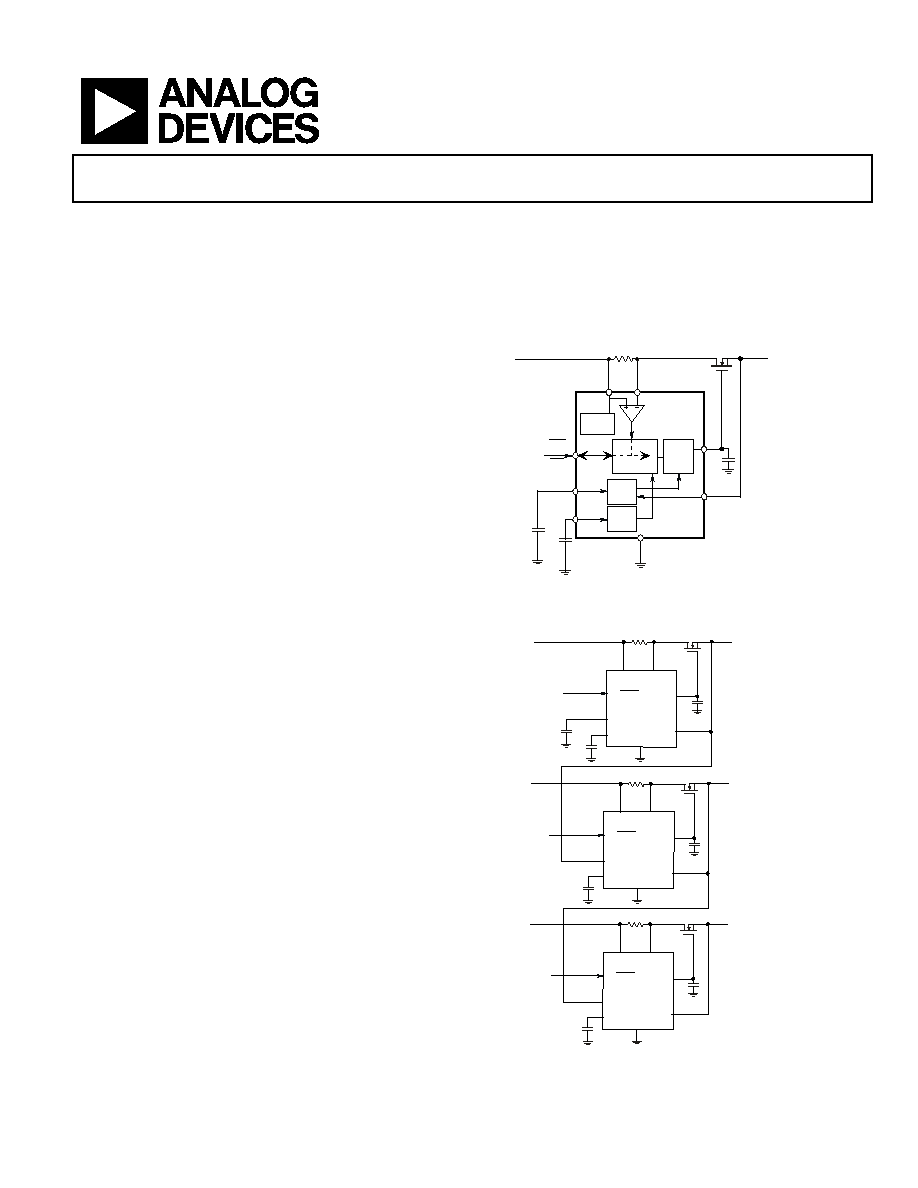
Functional Block Diagram
Q1
GATE
VCC
V
CC
V
OUT
GND
UP/DOWN
FET
DRIVER
V
OUT
LOGIC
V
IN
ADM1203
SLEW RATE
CONTROL
C
SLEW
C
SLEW
UP/STOP
(ADM1203-1/3)
(ADM1203-2/4)
20nF
R
s
TIMER
CONTROL
C
TIMER
C
TIMER
RS-
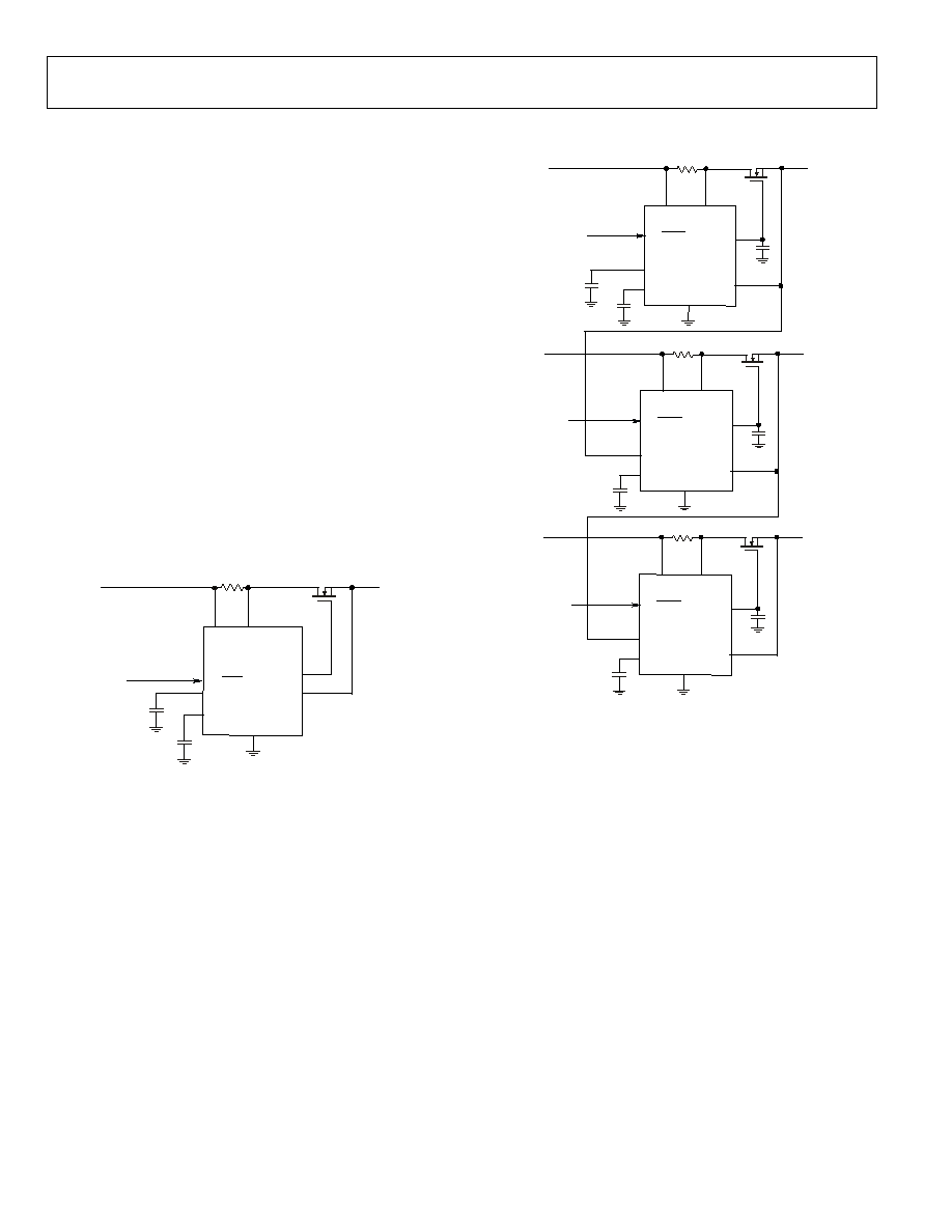
Applications Diagram
Q1
GATE
TIMER
UP/DOWN
V
OUTFB
5VIN
5VOUT
ADM1203-1
GND
POWER ON/OFF
1nF
C
TIMER
V
cc
SLEW
CSLEW
RS-
Q1
GATE
TIMER
UP/DOWN
V
OUTFB
3.3VIN
3.3VOUT
ADM1203-1
GND
POWER ON/OFF
1nF
C
TIMER
V
cc
SLEW
RS-
Q1
GATE
TIMER
UP/DOWN
V
OUTFB
2.7VIN
2.7VOUT
ADM1203-1
GND
POWER ON/OFF
1nF
C
TIMER
V
cc
SLEW
RS-
RSENSE
RSENSE
RSENSE
Rev. PrD
Information furnished by Analog Devices is believed to be accurate and reliable.
However, no responsibility is assumed by Analog Devices for its use, nor for any
infringements of patents or other rights of third parties that may result from its use.
Specifications subject to change without notice. No license is granted by implication
or otherwise under any patent or patent rights of Analog Devices. Trademarks and
registered trademarks are the property of their respective companies.
One Technology Way, P.O. Box 9106, Norwood, MA 02062-9106, U.S.A.
Tel: 781.329.4700
www.analog.com
Fax: 781.326.8703
© 2003 Analog Devices, Inc. All rights reserved.
© 2005

Rev. PrD | Page 2 of 8
ADM1203--SPECIFICATIONS
Table 1. V
CC
= Full Operating Range, T
A
= -40°C to +85°C, unless otherwise noted.
Parameter Min
Typ
Max
Units
Conditions
V
CC
Pin
Operating Voltage Range Vcc
2.7
16.5
V
Undervoltage Lockout, V
UVLO
2.4
2.525
2.65
V
Vcc Rising
UVLO
Hysteresis
25 mV
Switched Voltage Range
0.65
16.5
V
Quiesent Current
0.65
1.0
m
A
Up/Downb Pin
Input Threshold
0.58
0.6
0.62
V
Rising
Input Threshold Hysteresis
60
mV
Input Current
-100 100 nA
RS- Pin
Hot Swap Voltage
2.7
16.5
V
RS- Pin Input Current, I
INRS
TBD -200 TBD
µ
A
V
RS
= V
CC
, V
HOTSWAP
= 0.6 V,
10 20 30
µ
A
V
RS
= V
CC
, V
HOTSWAP
> 2.2 V
Circuit Breaker Limit Voltage, V
CB
34 47 60
mV
V
CB
= (V
CC
V
RS
) ,V
HOTSWAP
= 0.6 V
44 47 53
mV
V
CB
= (V
CC
V
RS
) ,V
HOTSWAP
> 2.2 V
Over Current Limit Voltage, V
OC
40 53 66
mV
V
HOTSWAP
= 0.6 V
50 53 59
mV
V
HOTSWAP
> 2.2 V
C
SLEW
Pin
Slew up Current
-10
µ
A
Slew down Current
10
µ
A
Tracking Gain
1
V/V
V
SLEW
/V
OUTFB
Minimum Tracking Voltage
0.1
V
Maximum Tracking voltage
Vcc 0.3
V
Slew Rate
100 1000
V/s
V
OUTFB
Pin
Input Current
-10 10
µ
A
Voltage Range
0
Vcc
V
GATE Pin
Gate Pullup Current
12
µ
A
Vslew Vout > 100mV
Gate Pulldown Current
12
µ
A
Vout Vslew > 100mV
Gate Pulldown Current
2
m
A
ADM1203-2 only vgate = 3.0V
GATE Voltage, V
GATE
5
6.5
10
V
V
GATE
V
CC
; V
CC
= 2.7V
6
8
12
V
V
GATE
V
CC
; V
CC
= 5.0V
5
6.5
10
V
V
GATE
V
CC
; V
CC
= 16.5V
TIMER Pin
TIMER Pin Pull-Up Current, I
TIMERUP
-4 -5 -6
µ
A
Initial Cycle, V
TIMER
= 1V
-48 -60 -72
µ
A
During Current Fault, V
TIMER
= 1V
TIMER Pin Pull-Down Current, I
TIMERDN
2
2.5
µ
A
After Current Fault, V
TIMER
= 1V
100
µ
A
Normal Operation, V
TIMER
= 1V
TIMER Pin Threshold High, V
TIMERH
1.235 1.3 1.365
V
TIMER rising
TIMER Pin Threshold Low, V
TIMERL
0.18
0.2
0.22
V
TIMER falling
NOTES:
Preliminary Technical Data

Preliminary Technical Data
ADM1203
Rev. PrD | Page 3 of 8
Absolute Maximum Ratings
Table 2. ADM1203 Absolute Maximum Ratings
Parameter
Rating
V
CC
Pin
20V
TIMER Pin
20V
UP/DOWNb, UP/STOPb
20V
RS- Pin
20V
C
SLEW
Pin
20V
Gate Pin
Vcc + 11V
V
OUTFB
Pin
20V
Power Dissipation
TBD
Storage Temperature
65°C to +125°C
Operating Temperature Range
40°C to +85°C
Lead Temperature Range
(Soldering 10 sec)
300°C
Junction Temperature
150°C
ADM1203
Preliminary Technical Data
Rev. PrD | Page 4 of 8
ENABLING A SINGLE SUPPLY
The ADM1203 requires a supply voltage of 2.7V to 16.5V on its
Vcc pin for operation. The device may be powered from the
input supply rail that is being switched or from an auxiliary
supply.
An internal charge pump ensures that the ADM1203 is capable
of fully enhancing an external FET via the GATE pin, turning
on the output. An external capacitor may be required on the
GATE node for stability.
Power up can be externally initiated by driving the
UP/DOWNb (ADM1203-1) or UP/STOPb (ADM12032)
logic pin high. A low on this pin will initiate a power down.
The V
OUTFB
pin monitors the output voltage.
A single ADM1203 device may be used where a single supply
rail is required to switch on at a controlled slew rate (see Figure
1). The value of the slew rate capacitor, C
SLEW
, will dictate the
slew rate of the GATE voltage at startup. An internal current
10
µ
A source charges C
SLEW
and the GATE voltage is ramped at
the same rate.
Q1
GATE
V
cc
C
SLEW
UP/STOP
V
OUT
3.3VIN
3.3VOUT
ADM1203-2
GND
POWER ON/OFF
C
SLEW
R
s
RS-
C
TIMER
C
TIMER
Figure 1. ADM1203 Switching on a Single Supply
MULTI-SUPPLY TRACKING
The primary function of the ADM1203 is to provide a voltage
tracking solution for multiple supply rails. The implementation
in Figure 2 will provide this function. Each voltage rail has its
own ADM1203 device driving a FET.
The UP/DOWNb (ADM1203-1/3) or UP/STOPb (ADM1203-
2/4) pins of all devices can be driven by a single logic input
which will initiate a system power-up going high or power-
down going low.
In figure 2, the ADM1203 is configured to control the ramp of
the largest supply first. The output of the first device is
connected to the slew pin on the second device to allow the rate
of the first supply to control the rate of the second and so on.
Q1
GATE
TIMER
UP/DOWN
V
OUTFB
5VIN
5VOUT
ADM1203-1
GND
POWER ON/OFF
1nF
C
TIMER
V
cc
SLEW
C
SLEW
RS-
Q1
GATE
TIMER
UP/DOWN
V
OUTFB
3.3VIN
3.3VOUT
ADM1203-1
GND
POWER ON/OFF
1nF
C
TIMER
V
cc
SLEW
RS-
Q1
GATE
TIMER
UP/DOWN
V
OUTFB
2.7VIN
2.7VOUT
ADM1203-1
GND
POWER ON/OFF
1nF
C
TIMER
V
cc
SLEW
RS-
R
S
R
S
R
S
Figure 2. ADM1203 Solution for Tracking 3 Supplies
A low-to-high transition on the UP/DOWNb or UP/STOPb pin
will initiate turn-on of the supplies. The ADM1203 will begin to
source current into the C
SLEW
capacitor. The voltages on all
GATE pins will begin to rise, or "track" up, at the same rate, as
set by the value of C
SLEW
. All supply voltages will remain within
100mV of the C
SLEW
voltage until they level off at their full
potentials.
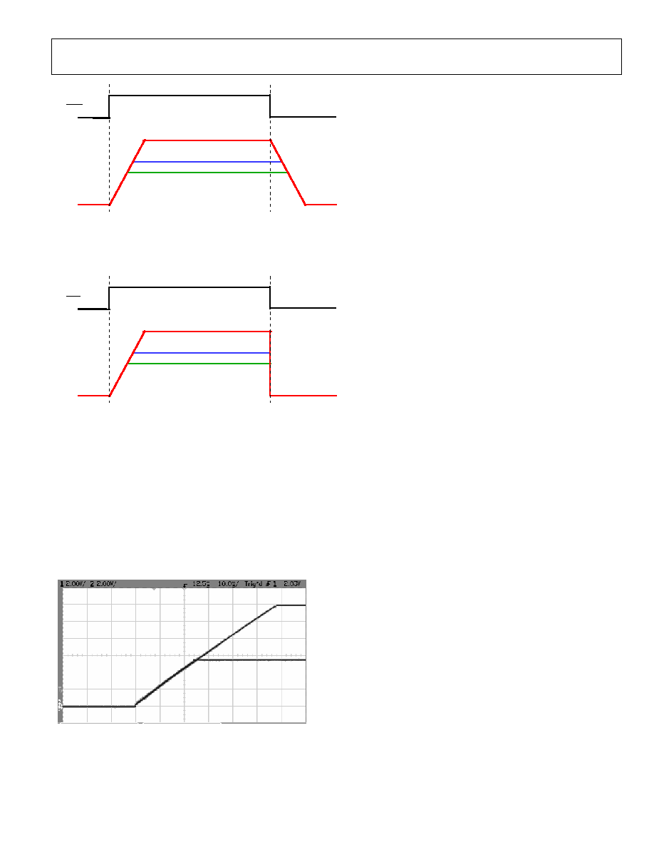
A high-to-low on the UP/DOWNb pin of the ADM1203-1 will
initiate a tracking down of the supply rails. The voltages will
attempt to stay with ~100mV of each other assuming the load
current will be sufficient to discharge the capacitors at the
required rate. (See Figure 3.)
A high-to-low on the UP/STOPb pin of the ADM1203-2 will
initiate an emergency fast shutdown of all supply rails
simultaneously. (See Figure 4.) Note that while the pass FETs
will be turned off immediately the actual discharge rate of each
supply rail will depend on the load.
Preliminary Technical Data
ADM1203
Rev. PrD | Page 5 of 8
2.5V
1.5V
3.3V
UP/DO WN
OUTP UT
VOLTAGE S
Figure 3. ADM1203-1 Power-Up and Power-Down Waveforms
2.5V
1.5V
3.3V
UP/STOP
OUTP UT
V OLTAGE S
Figure 4. ADM1203-2 Power-Up and Power-Down Waveforms
SLEW RATE CONTROL
Voltage tracking is achieved by controlling the slew rate of a
rising or falling supply by an external capacitor on the SLEW
pin. Alternatively, this pin can be overdriven with a supply
which will result in the output following this supply. The gate
responds to maintain ~100mV between the VOUTFB pin and
the SLEW pin
Figure 6. Tracking up Waveforms
CURRENT LIMIT CIRCUIT BREAKER FUNCTION
The ADM1203 features a current limiting circuit breaker.
When there is a sudden load current surge, such as a low
impedance fault, the bus supply voltage can drop significantly
to a point where the power to an adjacent card is
affected, causing system malfunctions. The ADM1203 fast
response current RS amplifier instantly limits current by
reducing the external FET GATE pin voltage. This
minimizes the bus supply voltage drop and permits power
budgeting and fault isolation without affecting neighboring
cards. A compensation circuit should be connected to
the GATE pin for current limit loop stability.
CALCULATING CURRENT LIMIT
The nominal fault current limit is determined by a RS
resistor connected between V
CC
and the RS- pin as
given by the equation below:
I
LIMIT(NOM)
= V
CB(NOM)
/ R
RS
(1)
The minimum load current is given by Equation 2:
I
LIMIT(MIN)
= V
CB(MIN)
/ R
RS(MAX)
(2)
The maximum load current is given by Equation 3:
I
LIMIT(MAX)
= V
CB(MAX)
/ R
RS(MIN)
(3)
Note: The power rating of the RS resistor should be rated at the
fault current level. The RS resistor power rating must exceed
V
CB(MAX
)
2
/R
RS(MIN).
ADM1203
Preliminary Technical Data
Rev. PrD | Page 6 of 8
TIMER FUNCTION
The TIMER pin handles several key functions with an external
capacitor, C
TIMER
. There are two comparator thresholds:
COMP1 (0.2V) and COMP2 (1.3V). The four timing current
sources are:
·
5µA pull-up
·
60µA pull-up
·
2µA pull-down
·
100µA pull-down
The 100µA is a non-ideal current source approximating a 7k
resistor below 0.4V.
INITIAL TIMING CYCLE
When the card is being inserted into the bus connector, the
long pins mate first which brings up the supply VIN at time
point 1 of Figure 7. The ADM1203 is in reset mode as the ON
pin is low. GATE is pulled low and the TIMER pin is pulled low
with a 100µA source. At time point 2, the short pin makes
contact and ON is pulled high. At this instant, a start-up check
requires that the supply voltage be above UVLO, the ON pin
beabove1.3Vand the TIMER pin voltage be less than 0.2V.
When these three conditions are fulfilled, the initial cycle
begins and the TIMER pin is pulled high with 5µA. At time
point 3, the TIMER reaches the COMP2 threshold and the first
portion of the initial cycle ends. The 100µA current source then
pulls down the TIMER pin until it reaches 0.2V at time point 4.
The initial cycle delay (time point 2 to time point 4) is related to
C
TIMER
by equation:
t
INITIAL
~= 272.9 x C
TIMER
ms/uF (4)
When the initial cycle terminates, a start-up cycle is activated
and the GATE pin ramps high. The TIMER pin continues to be
pulled down towards ground.
VIN
VON
VGATE
VOUT
RESET
MODE
VTIMER
INITIAL
CYCLE
START -UP
CYCLE
NORM AL
CYCLE
Figure 7: Normal Start-up
VIN
VON
VGATE
VOUT
RESET
MODE
VTIMER
INITIAL
CYCLE
START-UP
CYCLE
NORMAL
CYCLE
IRSENSE
5µA
100µA
60µA
2µA
100µA
VTH
Figure 8: Current Limiting at Start-up
Preliminary Technical Data
ADM1203
Rev. PrD | Page 7 of 8
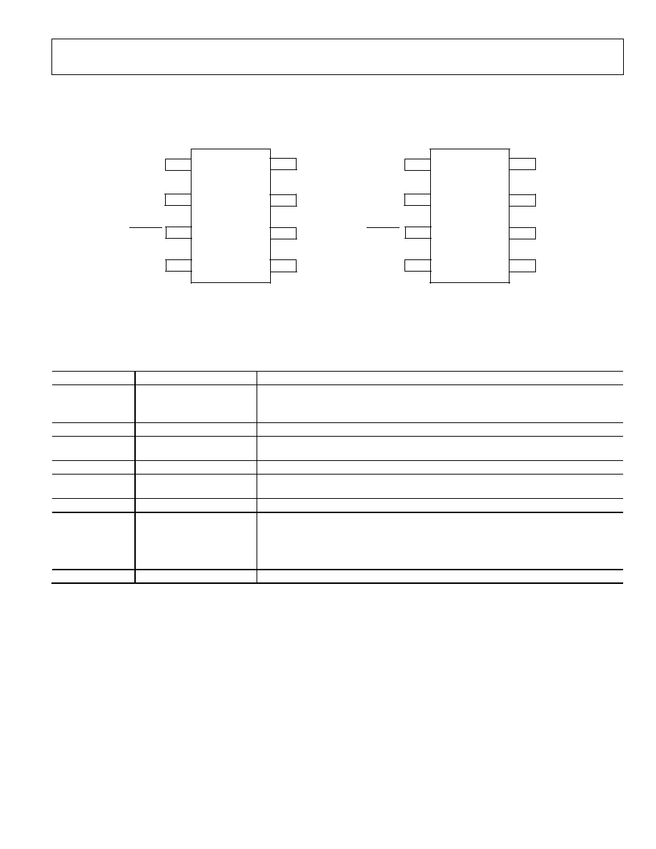
PIN CONFIGURATIONS
1
2
3
V
CC
RS-
GND
ADM1203-1AUJ
TOP VIEW
(Not to Scale)
C
SLEW
TIMER
8
7
GATE
V
OUT
4
5
6
UP / DOWN
1
2
3
V
CC
GND
ADM1203-2AUJ
TOP VIEW
(Not to Scale)
8
7
V
OUT
4
5
6
UP / STOP
TIMER
RS-
GATE
C
SLEW
PIN FUNCTIONAL DESCRIPTIONS
Pin No.
Name
Description
1 TIMER
Timer Input Pin. An external capacitor
C
TIMER
sets a 272.9ms/
µ
F initial timing delay and a
21.7ms/
µ
F circuit breaker delay. The GATE pin turns off whenever the TIMER pin is pulled
beyond the upper threshold, such as for overvoltage detection with an external zener.
2
GND
Chip Ground Pin.
3
UP/DOWNb or UP/STOPb
Logic Pin. Drive high to initiate track up off all ADM1203 controlled rails. Drive low to
initiate track down of all rails (ADM1203-1) or a fast shutdown of all rails (ADM1203-2).
4
VOUT
Monitors the Source of the external FET
5 CSLEW
Connect to an external capacitor to control the slew rate of the of the GATE at turn on
(and turn-off for ADM1203-1).
6
GATE
Drives the GATE node of the external FET
7 RS-
Current Limit Sense Input Pin. A sense resistor between the Vcc and RS- pins sets the
analog current limit. In overload, the EA controls the external FET gate to maintain the
SENSE voltage at 47mV. When the EA is maintaining current limit, the TIMER circuit
breaker mode is activated. The current limit loop/circuit breaker mode can be disabled
by connecting the Vcc pin and RS- pin together..
8
VCC
Chip Power Supply, 2.7V to 16.5V.
Rev. PrD | Page 8 of 8
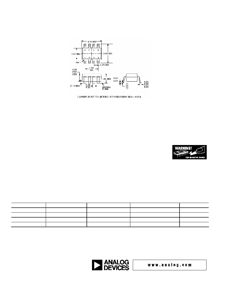
OUTLINE DIMENSIONS
Figure XX. 8-Lead TSOT Package (UJ-8)--Dimensions shown in millimeters
ESD CAUTION
ESD (electrostatic discharge) sensitive device. Electrostatic charges as high as 4000 V readily accumulate on the
human body and test equipment and can discharge without detection. Although this product features
proprietary ESD protection circuitry, permanent damage may occur on devices subjected to high energy
electrostatic discharges. Therefore, proper ESD precautions are recommended to avoid performance
degradation or loss of functionality.
Table 3. Ordering Guide
Part Number
Variant
Temperature Package
Package Description
Package Outline
ADM1203-1AUJ
UP/DOWNb logic input
40°C to +85°C
TSOT
UJ-8
ADM1203-2AUJ UP/STOPb
logic
input
40°C to +85°C
TSOT
UJ-8
ADM1203-3AUJ
UP/DOWNb logic input
40°C to +85°C
TSOT
UJ-8
ADM1203-4AUJ UP/STOPb
logic
input
40°C to +85°C
TSOT
UJ-8
003 Analog Devices, Inc. All rights reserved. Trademarks and
registered trademarks are the property of their respective companies.
Printed in the U.S.A.
Preliminary Technical Data
2005
PR05140-0-2/05(PrD)
ADM1203