Äîêóìåíòàöèÿ è îïèñàíèÿ www.docs.chipfind.ru
Simple Sequencers
TM
in 6-Lead SC70
ADM1085/ADM1086/ADM1087/ADM1088
Rev. 0
Information furnished by Analog Devices is believed to be accurate and reliable.
However, no responsibility is assumed by Analog Devices for its use, nor for any
infringements of patents or other rights of third parties that may result from its use.
Specifications subject to change without notice. No license is granted by implication
or otherwise under any patent or patent rights of Analog Devices. Trademarks and
registered trademarks are the property of their respective owners.
One Technology Way, P.O. Box 9106, Norwood, MA 02062-9106, U.S.A.
Tel: 781.329.4700
www.analog.com
Fax: 781.326.8703
© 2004 Analog Devices, Inc. All rights reserved.
FEATURES
Provide programmable time delays between enable
signals
Can be cascaded with power modules for multiple
supply sequencing
Power supply monitoring from 0.6 V
Output stages:
High voltage (up to 22 V) open-drain output
(ADM1085/ADM1087)
Push-pull output (ADM1086/ADM1088)
Capacitor-adjustable time delays
High voltage (up to 22 V) Enable and V
IN
inputs
Low power consumption (15 µA)
Specified over 40°C to +125°C temperature range
6-lead SC70 package
APPLICATIONS
Desktop/notebook computers, servers
Low power portable equipment
Routers
Base stations
Line cards
Graphics cards
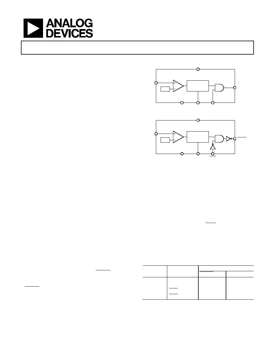
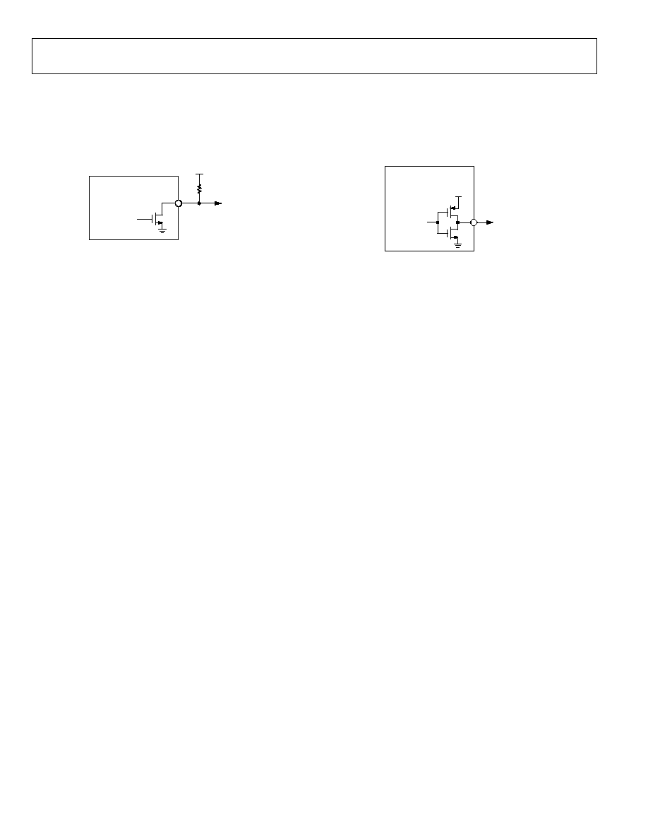
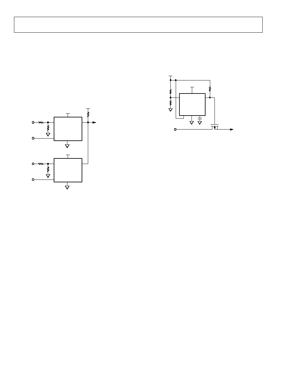
FUNCTIONAL BLOCK DIAGRAMS
04591-P
r
G-001
CAPACITOR
ADJUSTABLE
DELAY
0.6V
ADM1085/ADM1086
V
IN
ENOUT
ENIN
CEXT
V
CC
GND
CAPACITOR
ADJUSTABLE
DELAY
0.6V
ADM1087/ADM1088
V
IN
ENOUT
ENIN
CEXT
V
CC
GND
Figure 1.
GENERAL DESCRIPTION
The ADM1085/ADM1086/ADM1087/ADM1088 are simple
sequencing circuits that provide a time delay between the
enabling of voltage regulators and/or dc-dc converters at power-
up in multiple supply systems. When the output voltage of the
first power module reaches a preset threshold, a time delay is
initiated before an enable signal allows subsequent regulators to
power up. Any number of these devices can be cascaded with
regulators to allow sequencing of multiple power supplies.
Threshold levels can be set with a pair of external resistors in a
voltage divider configuration. By choosing appropriate resistor
values, the threshold can be adjusted to monitor voltages as low
as 0.6 V.
The ADM1086 and ADM1088 have push-pull output stages,
with active-high (ENOUT) and active-low (ENOUT) logic
outputs, respectively. The ADM1085 has an active-high
(ENOUT) logic output; the ADM1087 has an active-low
(ENOUT) output. Both the ADM1085 and ADM1087 have
open-drain output stages that can be pulled up to voltage levels
as high as 22 V through an external resistor. This level-shifting
property ensures compatibility with enable input logic levels of
different regulators and converters.
All four models have a dedicated enable input pin that allows
the output signal to the regulator to be controlled externally.
This is an active-high input (ENIN) for the ADM1085 and
ADM1086, and an active-low input (ENIN) for the ADM1087
and ADM1088.
The simple sequencers are specified over the extended -40°C to
+125°C temperature range. With low current consumption of 15
µA (typ) and 6-lead SC70 packaging, the parts are suitable for
low-power portable applications.
Table 1. Selection Table
Output Stage
Part No.
Enable Input
ENOUT
ENOUT
ADM1085
ENIN
Open-Drain
ADM1086
ENIN
Push-Pull
ADM1087
ENIN
Open-Drain
ADM1088
ENIN
Push-Pull

ADM1085/ADM1086/ADM1087/ADM1088
Rev. 0 | Page 2 of 16
TABLE OF CONTENTS
Specifications..................................................................................... 3
Absolute Maximum Ratings............................................................ 4
ESD Caution.................................................................................. 4
Pin Configuration and Function Descriptions............................. 5
Typical Performance Characteristics ............................................. 6
Circuit Information .......................................................................... 9
Timing Characteristics and Truth Tables.................................. 9
Capacitor-Adjustable Delay Circuit........................................... 9
Open-Drain and Push-Pull Outputs ....................................... 10
Application Information................................................................ 11
Sequencing Circuits ................................................................... 11
Dual LOFO Sequencing ............................................................ 13
Simultaneous Enabling.............................................................. 13
Power Good Signal Delays........................................................ 13
Quad-Supply Power Good Indicator....................................... 14
Sequencing with FET Switches................................................. 14
Outline Dimensions ....................................................................... 15
Ordering Guide .......................................................................... 15
REVISION HISTORY
7/04--Revision 0: Initial Version
ADM1085/ADM1086/ADM1087/ADM1088
Rev. 0 | Page 3 of 16
SPECIFICATIONS
V
CC
= full operating range, T
A
= -40°C to +125°C, unless otherwise noted.
Table 2.
Parameter
Min
Typ
Max
Unit
Test Conditions/Comments
SUPPLY
V
CC
Operating Voltage Range
2.25
3.6
V
V
IN
Operating Voltage Range
0
22
V
Supply Current
10
15
µA
V
IN
Rising Threshold, V
TH_RISING
0.56
0.6
0.64
V
V
CC
= 3.3 V
V
IN
Falling Threshold, V
TH_FALLING
0.545
0.585
0.625
V
V
CC
= 3.3 V
V
IN
Hysteresis
15
mV
V
IN
to ENOUT/ENOUT Delay
V
IN
Rising
35
µs
CEXT floating, C = 20 pF
2
ms
CEXT = 470 pF
V
IN
Falling
20
µs
V
IN
= V
TH_FALLING
to (V
TH_FALLING
100 mV)
V
IN
Leakage Current
170
µA
V
IN
= 22 V
CEXT Charge Current
125
250
375
nA
Threshold Temperature Coefficient
30
ppm/°C
ENIN/ENIN TO ENOUT/ENOUT Propagation
Delay
0.5
µs
V
IN
> V
TH_RISING
ENIN/ENIN Voltage Low
0.3
V
CC
- 0.2
V
ENIN/ENIN Voltage High
0.3 V
CC
+ 0.2
V
ENIN/ENIN Leakage Current
170
µA
ENIN/ENIN = 22 V
ENOUT/ENOUT Voltage Low
0.4
V
V
IN
< V
TH_FALLING
(ENOUT),
V
IN
> V
TH_RISING
(ENOUT),
I
SINK
= 1.2 mA
ENOUT/ENOUT Voltage High
(ADM1086/ADM1088)
0.8 V
CC
V
V
IN
> V
TH_RISING
(ENOUT),
V
IN
< V
TH_FALLING
(ENOUT),
I
SOURCE
= 500 µA
ENOUT/ENOUT Open-Drain Output Leakage
Current (ADM1085/ADM1087)
0.4
µA
ENOUT/ENOUT = 22 V
ADM1085/ADM1086/ADM1087/ADM1088
Rev. 0 | Page 4 of 16
ABSOLUTE MAXIMUM RATINGS
T
A
= 25°C, unless otherwise noted.
Table 3.
Parameter Rating
V
CC
-0.3 V to +6 V
V
IN
-0.3 V to +25 V
CEXT
-0.3 V to +6 V
ENIN, ENIN
-0.3 V to +25 V
ENOUT, ENOUT (ADM1085, ADM1087)
-0.3 V to +25 V
ENOUT, ENOUT (ADM1086, ADM1088)
-0.3 V to +6 V
Operating Temperature Range
-40°C to +125°C
Storage Temperature Range
-65°C to +150°C
JA
Thermal Impedance, SC70
146°C/W
Lead Temperature
Soldering (10 s)
300°C
Vapor Phase (60 s)
215°C
Infrared (15 s)
220°C
Stresses above those listed under Absolute Maximum Ratings
may cause permanent damage to the device. This is a stress
rating only and functional operation of the device at these or
any other conditions above those indicated in the operational
section of this specification is not implied. Exposure to absolute
maximum rating conditions for extended periods may affect
device reliability.
ESD CAUTION
ESD (electrostatic discharge) sensitive device. Electrostatic charges as high as 4000 V readily accumulate on
the human body and test equipment and can discharge without detection. Although this product features
proprietary ESD protection circuitry, permanent damage may occur on devices subjected to high energy
electrostatic discharges. Therefore, proper ESD precautions are recommended to avoid performance
degradation or loss of functionality.
ADM1085/ADM1086/ADM1087/ADM1088
Rev. 0 | Page 5 of 16
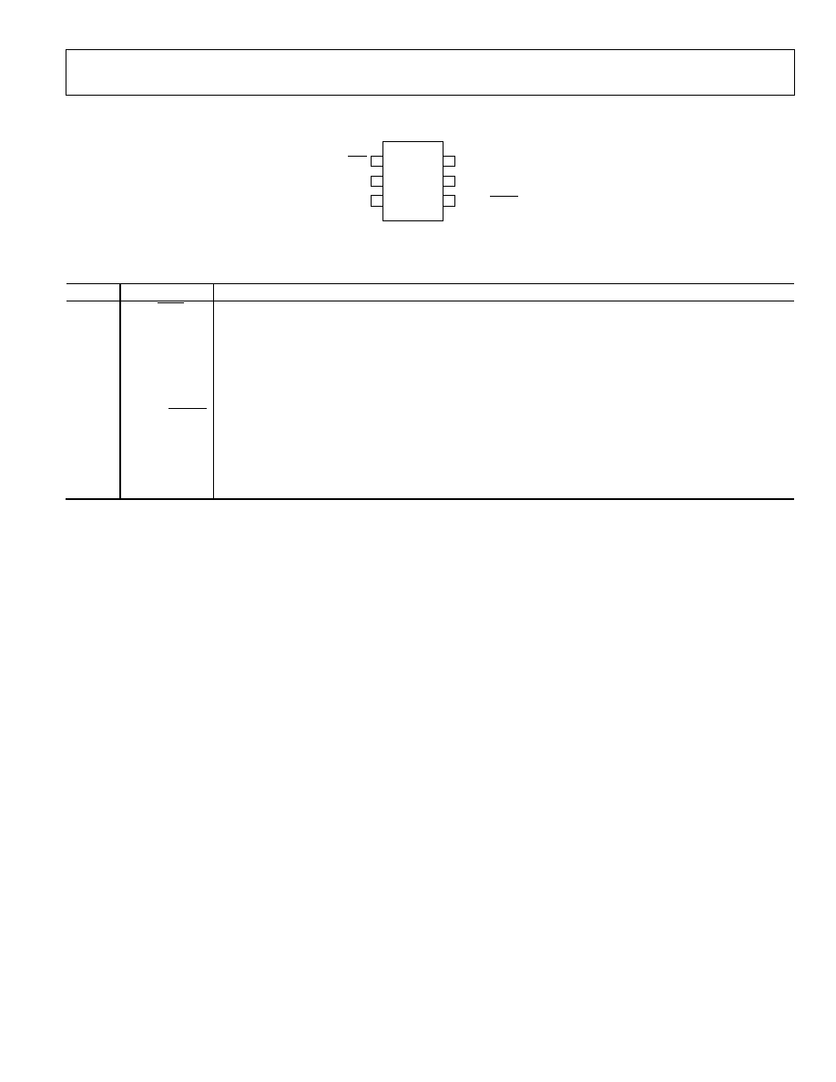
PIN CONFIGURATION AND FUNCTION DESCRIPTIONS
04591-P
r
G-002
ENIN/ENIN
1
GND
2
V
IN
3
V
CC
6
CEXT
5
ENOUT/ENOUT
4
ADM1085/
ADM1086/
ADM1087/
ADM1088
TOP VIEW
(Not to Scale)
Figure 2. Pin Configuration
Table 4. Pin Function Descriptions
Pin No.
Mnemonic
Description
1
ENIN, ENIN
Enable Input. Controls the status of the enable output. Active high for ADM1085/ADM1086. Active low for
ADM1087/ADM1088.
2 GND
Ground.
3 V
IN
Input for the Monitored Voltage Signal. Can be biased via a voltage divider resistor network to customize the
effective input threshold. Can precisely monitor an analog power supply output signal and detect when it has
powered up. The voltage applied at this pin is compared with a 0.6 V on-chip reference. With this reference,
digital signals with various logic-level thresholds can also be detected.
4
ENOUT, ENOUT Enable Output. Asserted when the voltage at V
IN
is above V
TH_RISING
and the time delay has elapsed, provided
that the enable input is asserted. Active high for the ADM1085/ADM1086. Active low for the
ADM1087/ADM1088.
5 CEXT
External Capacitor Pin. The capacitance on this pin determines the time delay on the enable output. The delay
is seen only when the voltage at V
IN
rises past V
TH_RISING
, and not when it falls below V
TH_FALLING
.
6 V
CC
Power Supply.
ADM1085/ADM1086/ADM1087/ADM1088
Rev. 0 | Page 6 of 16
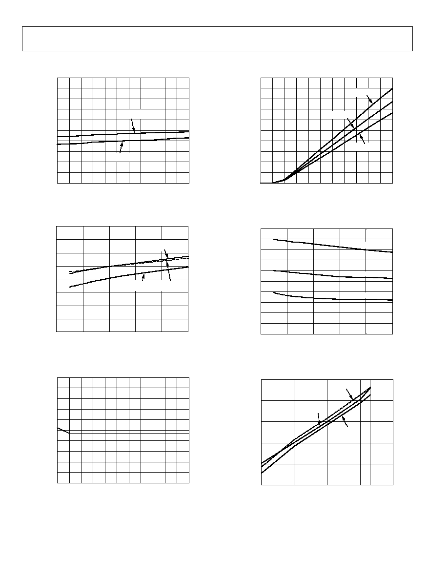
TYPICAL PERFORMANCE CHARACTERISTICS
700
500
520
540
560
580
600
620
640
660
680
40 25 10
5
20
35
50
65
80
95
110 125
04591-P
r
G-003
TEMPERATURE (
°
C)
V
TRIP
(mV
)
V
TRIP
RISING
V
TRIP
FALLING
Figure 3. V
IN
Threshold vs. Temperature
12.0
8.0
8.5
9.0
9.5
10.0
10.5
11.0
11.5
2.10
2.40
2.70
3.00
3.30
3.60
04591-P
r
G-004
V
CC
(V)
I
CC
(
µ
A)
T
A
= +125
°
C
T
A
= +25
°
C
T
A
= 40
°
C
Figure 4. Supply Current vs. Supply Voltage
20
18
16
14
12
10
8
6
4
2
0
0
2
4
6
8
10
12
14
16
18
20
22
04591-P
r
G-005
V
IN
(V)
S
U
P
P
L
Y
CURRE
NT (
µ
A)
Figure 5. Supply Current vs. V
IN
Voltage
200
180
160
140
120
100
80
60
40
20
0
0
2
4
6
8
10
12
14
16
18
20
22
04591-P
r
G-006
V
IN
(V)
V
IN
LE
AKAGE
CURRE
NT (
µ
A)
T
A
= +125
°
C
T
A
= +25
°
C
T
A
= 40
°
C
Figure 6. V
IN
Leakage Current vs. V
IN
Voltage
200
190
180
170
160
150
140
130
120
110
100
2.10
3.60
3.30
3.00
2.70
2.40
04591-P
r
G-007
V
CC
(V)
V
IN
LE
AKAGE
CURRE
NT (
µ
A)
T
A
= +125
°
C
T
A
= +25
°
C
T
A
= 40
°
C
Figure 7. V
IN
Leakage Current vs. V
CC
Voltage
10000
1
10
100
1000
0.1
0.01
100
20
10
1
0.1
04591-P
r
G-008
OUTPUT SINK CURRENT (mA)
OUTPUT VOLTAGE (mV)
T
A
= +125
°
C
T
A
= +25
°
C
T
A
= 40
°
C
Figure 8. Output Voltage vs. Output Sink Current
ADM1085/ADM1086/ADM1087/ADM1088
Rev. 0 | Page 7 of 16
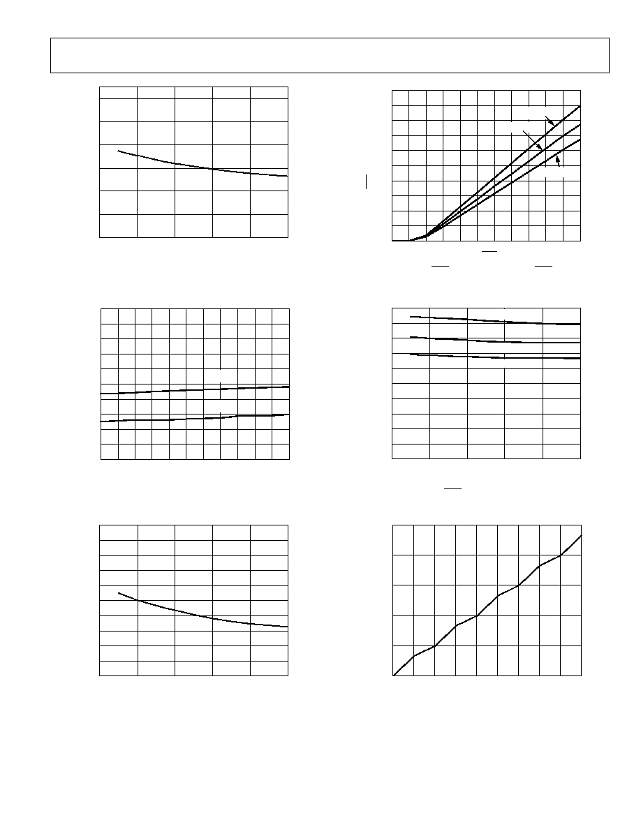
120
100
80
60
40
20
0
2.10
2.40
2.70
3.00
3.30
3.60
04591-P
r
G-009
SUPPLY VOLTAGE (V)
OU
TPU
T
LOW
VOLTA
G
E (
m
V)
Figure 9. Output Low Voltage vs. Supply Voltage
100
0
10
20
30
40
50
60
70
80
90
40 25 10
5
20
35
50
65
80
95
110 125
04591-P
r
G-010
TEMPERATURE (
°
C)
P
R
OP
AGATION DE
LAY
(
µ
s)
1mV/
µ
s
10mV/
µ
s
Figure 10. V
CC
Falling Propagation Delay vs. Temperature
500
450
400
350
300
250
200
150
100
50
0
2.10
2.40
2.70
3.00
3.30
3.60
04591-P
r
G-011
SUPPLY VOLTAGE (V)
FALL TIME (ns)
Figure 11. Output Fall Time vs. Supply Voltage
200
180
160
140
120
100
80
60
40
20
0
0
2
4
6
8
10
12
14
16
18
20
22
04591-P
r
G-012
ENIN/ENIN (V)
ENIN/ENIN LEAKAGE (
µ
A)
T
A
= +125
°
C
T
A
= +25
°
C
T
A
= 40
°
C
Figure 12. ENIN/ENIN Leakage Current vs. ENIN/ENIN Voltage
200
180
160
140
120
100
80
60
40
20
0
2.10
3.60
3.30
3.00
2.70
2.40
04591-P
r
G-013
V
CC
(V)
E
N
IN LE
AKAGE
(
µ
A)
T
A
= +125
°
C
T
A
= +25
°
C
T
A
= 40
°
C
Figure 13. ENIN/ENIN Leakage Current vs. V
CC
Voltage
10000
1000
100
10
1
0.1
0.562
26200
4480
2350
520
241
53.2
22.9
5.02
2.390
04591-P
r
G-014
TIMEOUT DELAY (ms)
C
EXT
(nF)
Figure 14. CEXT Capacitance vs. Timeout Delay
ADM1085/ADM1086/ADM1087/ADM1088
Rev. 0 | Page 8 of 16
300
100
120
140
160
180
200
220
240
260
280
40 25 10
5
20
35
50
65
80
95
110 125
04591-P
r
G-015
TEMPERATURE (
°
C)
CHARGE
CURRE
NT (nA)
Figure 15. CEXT Charge Current vs. Temperature
100
0
10
20
30
40
50
60
70
80
90
40 25 10
5
20
35
50
65
80
95
110 125
04591-P
r
G-016
TEMPERATURE (
°
C)
P
R
OP
AGATION DE
LAY
(
µ
s)
Figure 16. V
IN
to ENOUT/ENOUT Propagation Delay
(CEXT Floating) vs. Temperature
100
0
10
20
30
40
50
60
70
80
90
1
10
100
1000
04591-P
r
G-017
COMPARATOR OVERDRIVE (mV)
TRANS
IE
NT DURATION (
µ
s)
Figure 17. Maximum V
IN
Transient Duration vs. Comparator Overdrive
ADM1085/ADM1086/ADM1087/ADM1088
Rev. 0 | Page 9 of 16
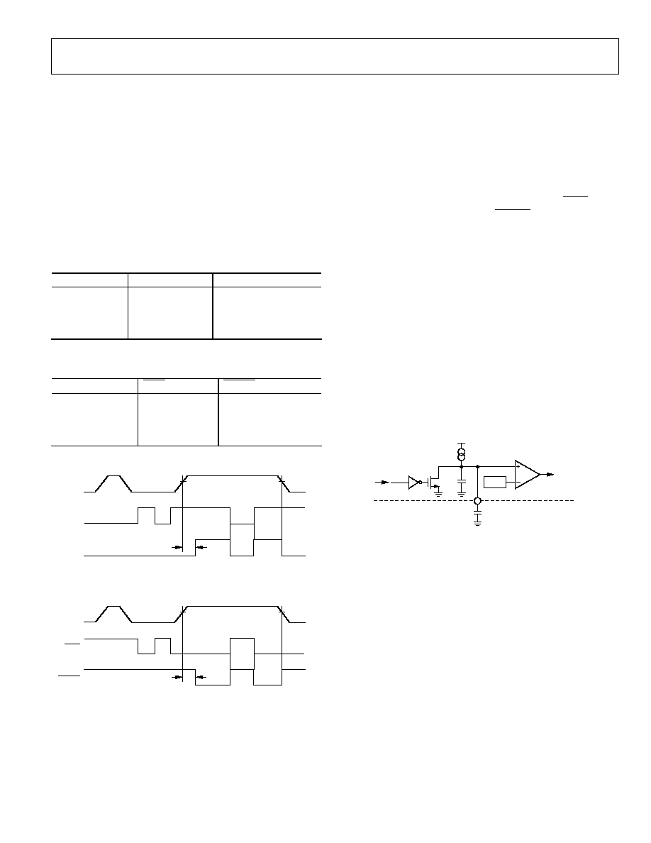
CIRCUIT INFORMATION
TIMING CHARACTERISTICS AND TRUTH TABLES
The enable outputs of the ADM1085/ADM1086/ADM1087/
ADM1088 are related to the V
IN
and enable inputs by a simple
AND function. The enable output is asserted only if the enable
input is asserted and the voltage at V
IN
is above V
TH_RISING
, with
the time delay elapsed. Table 5 and Table 6 show the enable
output logic states for different V
IN
/enable input combinations
when the capacitor delay has elapsed. The timing diagrams in
Figure 18 and Figure 19 give a graphical representation of how
the ADM1085/ADM1086/ADM1087/ADM1088 enable outputs
respond to V
IN
and enable input signals.
Table 5. ADM1085/ADM1086 Truth Table
V
IN
ENIN ENOUT
<V
TH_FALLING
0
0
<V
TH_FALLING
1
0
>V
TH_RISING
0
0
>V
TH_RISING
1
1
Table 6. ADM1087/ADM1088 Truth Table
V
IN
ENIN
ENOUT
<V
TH_FALLING
1
1
<V
TH_FALLING
0
1
>V
TH_RISING
1
1
>V
TH_RISING
0
0
04591-P
r
G-023
V
IN
ENIN
ENOUT
t
EN
V
TH_RISING
V
TH_FALLING
Figure 18. ADM1085/ADM1086 Timing Diagram
04591-PrG
-
024
V
IN
ENIN
ENOUT
t
EN
V
TH_RISING
V
TH_FALLING
Figure 19. ADM1087/ADM1088 Timing Diagram
When V
IN
reaches the upper threshold voltage (V
TH_RISING
), an
internal circuit generates a delay (t
EN
) before the enable output
is asserted. If V
IN
drops below the lower threshold voltage
(V
TH_FALLING
), the enable output is deasserted immediately.
Similarly, if the enable input is disabled while V
IN
is above the
threshold, the enable output deasserts immediately. Unlike V
IN
, a
low-to-high transition on ENIN (or high-to-low on ENIN) does
not yield a time delay on ENOUT (ENOUT).
CAPACITOR-ADJUSTABLE DELAY CIRCUIT
Figure 20 shows the internal circuitry used to generate the time
delay on the enable output. A 250 nA current source charges a
small internal parasitic capacitance, C
INT
. When the capacitor
voltage reaches 1.2 V, the enable output is asserted. The time
taken for the capacitor to reach 1.2 V, in addition to the propa-
gation delay of the comparator, constitutes the enable timeout,
which is typically 35 µs.
To minimize the delay between V
IN
falling below V
TH_FALLING
and
the enable output de-asserting, an NMOS transistor is con-
nected in parallel with C
INT
. The output of the voltage detector
is connected to the gate of this transistor so that, when V
IN
falls
below V
TH_FALLING
, the transistor switches on and C
INT
discharges
quickly.
04591-P
r
G-024
1.2V
C
C
INT
CEXT
SIGNAL FROM
VOLTAGE
DETECTOR
TO AND GATE
AND OUTPUT
STAGE
V
CC
250nA
Figure 20. Capacitor-Adjustable Delay Circuit
Connecting an external capacitor to the CEXT pin delays the
rise time--and therefore the enable timeout--further. The
relationship between the value of the external capacitor and the
resulting timeout is characterized by the following equation:
t
EN
= (C × 4.8 ×10
6
) + 35 µs
ADM1085/ADM1086/ADM1087/ADM1088
Rev. 0 | Page 10 of 16
OPEN-DRAIN AND PUSH-PULL OUTPUTS
The ADM1085 and ADM1087 have open-drain output stages
that require an external pull-up resistor to provide a logic-high
voltage level. The geometry of the NMOS transistor enables the
output to be pulled up to voltage levels as high as 22 V.
04591-P
r
G-026
ADM1085/ADM1087
LOGIC
V
CC
(
22V)
Figure 21. Open-Drain Output Stage
The ADM1086 and ADM1088 have push-pull (CMOS) output
stages that require no external components to drive other logic
circuits. An internal PMOS pull-up transistor provides the
logic-high voltage level.
04591-P
r
G-027
ADM1086/ADM1088
V
CC
LOGIC
Figure 22. Push-Pull Output Stage
ADM1085/ADM1086/ADM1087/ADM1088
Rev. 0 | Page 11 of 16
APPLICATION INFORMATION
SEQUENCING CIRCUITS
The ADM1085/ADM1086/ADM1087/ADM1088 are
compatible with voltage regulators and dc-to-dc converters that
have active-high or active-low enable or shutdown inputs, with
a choice of open-drain or push-pull output stages. Figure 23 to
Figure 25 illustrate how each of the ADM1085/ADM1086/
ADM1087/ADM1088 simple sequencers can be used in
multiple-supply systems, depending on which regulators are
used and which output stage is preferred.
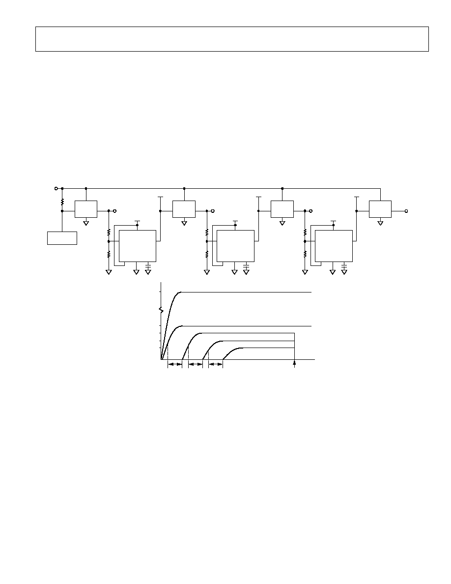
In Figure 23, three ADM1085s are used to sequence four
supplies on power-up. Separate capacitors on the CEXT pins
determine the time delays between enabling of the 3.3 V, 2.5 V,
1.8 V, and 1.2 V supplies. Because the dc/dc converters and
ADM1085s are connected in cascade, and the output of any
converter is dependent on that of the previous one, an external
controller can disable all four supplies simultaneously by
disabling the first dc/dc converter in the chain.
For power-down sequencing, an external controller dictates
when the supplies are switched off by accessing the ENIN
inputs individually.
04591-P
r
G-028
3.3V
DC/DC
IN
OUT
EN
ADM1085
V
CC
ENOUT
3.3V
ENIN
CEXT
V
IN
3.3V
2.5V
DC/DC
IN
OUT
EN
ADM1085
V
CC
ENOUT
3.3V
ENIN
CEXT
V
IN
3.3V
1.8V
DC/DC
IN
OUT
EN
ADM1085
V
CC
ENOUT
3.3V
ENIN
CEXT
V
IN
3.3V
1.2V
DC/DC
IN
OUT
EN
ENABLE
CONTROL
12V
t
EN1
t
EN2
t
EN3
EXTERNAL
DISABLE
12V
3.3V
2.5V
1.8V
1.2V
Figure 23. Typical ADM1085 Application Circuit
ADM1085/ADM1086/ADM1087/ADM1088
Rev. 0 | Page 12 of 16
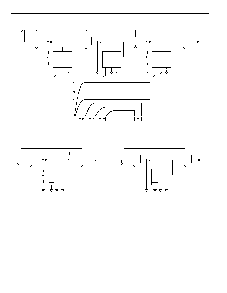
04591-P
r
G-029
3.3V
DC/DC
IN
OUT
EN
ADM1086
V
CC
ENOUT
3.3V
ENIN
CEXT
V
IN
2.5V
DC/DC
IN
OUT
EN
ADM1086
V
CC
ENOUT
3.3V
ENIN
CEXT
V
IN
1.8V
DC/DC
IN
OUT
EN
ADM1086
V
CC
ENOUT
3.3V
ENIN
CEXT
V
IN
1.2V
DC/DC
IN
OUT
EN
ENABLE
CONTROL
12V
t
EN1
t
EN2
t
EN3
EXTERNAL
DISABLE
12V
3.3V
2.5V
1.8V
1.2V
Figure 24. Typical ADM1086 Application Circuit
04591-P
r
G-030
3.3V
ADP3334
IN
OUT
SD
ADM1087
V
CC
ENOUT
3.3V
ENIN
CEXT
V
IN
2.5V
ADP3334
IN
OUT
SD
12V
Figure 25. Typical ADM1087 Application Circuit Using
ADP3334 Voltage Regulators
04591-P
r
G-031
3.3V
ADP3334
IN
OUT
SD
ADM1088
V
CC
ENOUT
3.3V
ENIN
CEXT
V
IN
2.5V
ADP3334
IN
OUT
SD
12V
Figure 26. Typical ADM1088 Application Circuit Using
ADP3334 Voltage Regulators
ADM1085/ADM1086/ADM1087/ADM1088
Rev. 0 | Page 13 of 16
DUAL LOFO SEQUENCING
A power sequencing solution for a portable device, such as a
PDA, is shown in Figure 27. This solution requires that the
microprocessor's power supply turn on before the LCD display
turns on, and that the LCD display power-down before the
microprocessor powers down. In other words, the last power
supply to turn on is the first one to turn off (LOFO).
An RC network connects the battery and the SD input of the
ADP3333 voltage regulator. This causes power-up and power-
down transients to appear at the SD input when the battery is
connected and disconnected. The 3.3 V microprocessor supply
turns on quickly on power-up and turns off slowly on power-
down. This is due to two factors: Capacitor C1 charges up to 9 V
on power-up and charges down from 9 V on power-down, and
the SD pin has logic-high and logic-low input levels of 2 V and
0.4 V.
For the display power sequencing, the ADM1085 is equipped
with capacitor C2, which creates the delay between the micro-
processor and display power turning on. When the system is
powered down, the ADM1085 turns off the display power
immediately, while the 3.3 V regulator waits for C1 to discharge
to 0.4 V before switching off.
04591-P
r
G-032
ADM1086
ENOUT
3.3V
C2
ENIN
CEXT
V
IN
C1
DISPLAY
POWER
ADP3333
5V
SD
9V
MICROPROCESSOR
POWER
ADP3333
2.5V
SD
9V
9V
SYSTEM
POWER SWITCH
SYSTEM
POWER
9V
0V
9V
0V
2.5V
0V
5V
0V
V
C1
MICROPROCESSOR
POWER
DISPLAY
POWER
Figure 27. Dual LOFO Power-Supply Sequencing
SIMULTANEOUS ENABLING
The enable output can drive multiple enable or shutdown
regulator inputs simultaneously.
04591-P
r
G-033
3.3V
ADP3333
IN
OUT
SD
ADM1085
V
CC
ENOUT
3.3V
3.3V
ENIN
CEXT
V
IN
2.5V
ADP3333
IN
OUT
SD
ENABLE
CONTROL
12V
1.8V
ADP3333
IN
OUT
SD
12V
Figure 28. Enabling a Pair of Regulators from a Single ADM1085
POWER GOOD SIGNAL DELAYS
Sometimes sequencing is performed by asserting Power Good
signals when the voltage regulators are already on, rather than
sequencing the power supplies directly. In these scenarios, a
simple sequencer IC can provide variable delays so that
enabling separate circuit blocks can be staggered in time.
For example, in a notebook PC application, a dedicated
microcomputer asserts a Power Good signal for North BridgeTM
and South BridgeTM ICs. The ADM1086 delays the south bridge's
signal, so that it is enabled after the north bridge.
04591-P
r
G-034
ADM1086
SOUTH
BRIDGE
IC
ENOUT
EN
5V
ENIN
CEXT
V
IN
NORTH
BRIDGE
IC
EN
5V
MICROCOMPUTER
5V
3.3V
POWER_GOOD
Figure 29. Power Good Delay
ADM1085/ADM1086/ADM1087/ADM1088
Rev. 0 | Page 14 of 16
QUAD-SUPPLY POWER GOOD INDICATOR
The enable output of the simple sequencers is equivalent to an
AND function of V
IN
and ENIN. ENOUT is high only when the
voltage at V
IN
is above the threshold and the enable input
(ENIN) is high as well. Although ENIN is a digital input, it can
tolerate voltages as high as 22 V and can detect if a supply is
present. Therefore, a simple sequencer can monitor two supplies
and assert what can be interpreted as a Power Good signal
when both supplies are present. The outputs of two ADM1085s
can be wire-ANDed together to make a quad-supply Power
Good indicator.
04591-PrG
-
035
ADM1085
ENOUT
3.3V
3.3V
ENIN
V
IN
9V
5V
ADM1085
ENOUT
3.3V
ENIN
V
IN
2.5V
1.8V
POWER_GOOD
Figure 30. Quad-Supply Power Good Indicator
SEQUENCING WITH FET SWITCHES
The open-drain outputs of the ADM1085 and ADM1087 can
drive external FET transistors, which can switch on power-
supply rails. All that is needed is a pull-up resistor to a voltage
source that is high enough to turn on the FET.
04591-
Pr
G-
036
ADM1085
ENOUT
3.3V
12V
ENIN
CEXT
V
IN
2.5V
Figure 31. Sequencing with a FET Switch
ADM1085/ADM1086/ADM1087/ADM1088
Rev. 0 | Page 15 of 16
OUTLINE DIMENSIONS
0.22
0.08
0.46
0.36
0.26
8°
4°
0°
0.30
0.15
1.00
0.90
0.70
SEATING
PLANE
1.10 MAX
2.00 BSC
PIN 1
2.10 BSC
0.65 BSC
1.25 BSC
1.30 BSC
0.10 MAX
0.10 COPLANARITY
COMPLIANT TO JEDEC STANDARDS MO-203AB
3
5
4
2
6
1
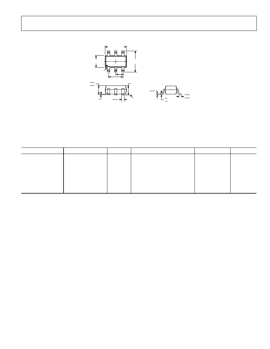
Figure 32. 6-Lead Plastic Surface-Mount Package [SC70]
(KS-6)
Dimensions shown in millimeters
ORDERING GUIDE
Model
Temperature Range
Quantity
Package Description
Package Option
Branding
ADM1085AKS-REEL7
-40°C to +125°C
3k
6-Lead Thin Shrink Small Outline
Transistor Package (SC70)
KS-6 M0V
ADM1086AKS-REEL7
-40°C to +125°C
3k
6-Lead Thin Shrink Small Outline
Transistor Package (SC70)
KS-6 M0W
ADM1087AKS-REEL7
-40°C to +125°C
3k
6-Lead Thin Shrink Small Outline
Transistor Package (SC70)
KS-6 M0X
ADM1088AKS-REEL7
-40°C to +125°C
3k
6-Lead Thin Shrink Small Outline
Transistor Package (SC70)
KS-6 M0Y

ADM1085/ADM1086/ADM1087/ADM1088
Rev. 0 | Page 16 of 16
NOTES
© 2004 Analog Devices, Inc. All rights reserved. Trademarks and
registered trademarks are the property of their respective owners.
D0459107/04(0)
Document Outline
- FEATURES
- APPLICATIONS
- GENERAL DESCRIPTION
- FUNCTIONAL BLOCK DIAGRAMS
- þÿ
- þÿ
- þÿ
- þÿ
- þÿ
- þÿ
- þÿ