LF to 4 GHz
High Linearity Y-Mixer
Preliminary Technical Data
ADL5350
Rev. PrC
Information furnished by Analog Devices is believed to be accurate and reliable. However, no
responsibility is assumed by Analog Devices for its use, nor for any infringements of patents or other
rights of third parties that may result from its use. Specifications subject to change without notice. No
license is granted by implication or otherwise under any patent or patent rights of Analog Devices.
Trademarks and registered trademarks are the property of their respective owners.
One Technology Way, P.O. Box 9106, Norwood, MA 02062-9106, U.S.A.
Tel: 781.329.4700
www.analog.com
Fax: 781.461.3113
© 2005 Analog Devices, Inc. All rights reserved.
FEATURES
Broadband RF, IF, and LO ports
Conversion loss: 6 dB
Noise figure: 6 dB
High input IP3: 26 dBm
High input P
1dB
: 17 dBm
Low LO drive level
Single-ended design: no need for baluns
Single-supply operation: 3 V @ 10 mA
Miniature 8-lead 3 mm x 2 mm LFCSP package
RoHS compliant
APPLICATIONS
Cellular base station
Point-to-point radio links
RF instrumentation
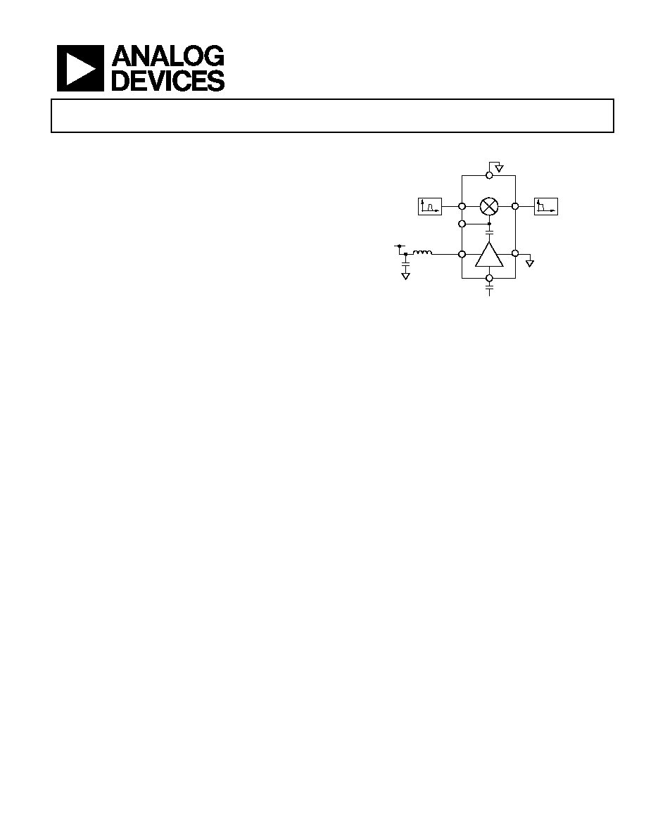
FUNCTIONAL BLOCK DIAGRAM
05
61
5-
0
0
1
RF
INPUT OR
OUTPUT
IF
OUTPUT OR
INPUT
3V
RF
IF
GND
GND
LO
LO
INPUT
VPOS
GC
ADL5350
Figure 1.
GENERAL DESCRIPTION
The ADL5350 is a high linearity, up-and-down converting mixer
capable of operating over a broad input frequency range. It is well
suited for demanding cellular base-station mixer designs that
require high sensitivity and efficient blocker immunity. Based
on a GaAs pHEMT single-ended mixer architecture, the ADL5350
provides excellent input linearity and low noise figure without
the need for a high power level, local oscillator (LO) drive.
In 850 MHz/900 MHz receive applications, the ADL5350
provides a typical conversion loss of only 6 dB. The integrated
LO amplifier allows a low LO drive level, typically only 4 dBm
for most applications. The input IP3 is typically greater than
25 dBm, with an input compression point of 17 dBm. The high
input linearity of the ADL5350 makes the device an excellent
mixer for communications systems that require high blocker
immunity, such as GSM 850/900 and 800 MHz CDMA2000. At
2 GHz, a slightly greater supply current is required to obtain
similar performance.
For low frequency applications, the ADL5350 provides access to
the gate contact of the output-mixing device. This allows an
external LO coupling capacitor to be applied between the
VPOS pin and GC pin, helping to improve the LO drive to the
switching device. Using a single 100 pF capacitor allows high
performance at the lower LO frequencies.
The single-ended broadband RF/IF port allows the device to be
customized for a desired band of operation using simple
external filter networks. The LO to RF isolation is based on the
LO rejection of the RF port filter network. Greater isolation
may be achieved using higher order filter networks as described
in the Applications section of this data sheet.
The ADL5350 is fabricated on a GaAs pHEMT high
performance IC process. The ADL5350 is available in a
3 mm × 2 mm 8-lead LFCSP package. It operates over a
-40°C to +85°C temperature range. An evaluation board is also
available.

ADL5350
Preliminary Technical Data
Rev. PrC | Page 2 of 24
TABLE OF CONTENTS
Features .............................................................................................. 1
Applications....................................................................................... 1
Functional Block Diagram .............................................................. 1
General Description ......................................................................... 1
Specifications..................................................................................... 3
820 MHz Receive Performance .................................................. 3
1950 MHz Receive Performance ................................................ 3
Spur Tables......................................................................................... 4
450 MHz Spur Table..................................................................... 4
820 MHz Spur Table..................................................................... 4
1950 MHz Spur Table................................................................... 5
Absolute Maximum Ratings............................................................ 6
ESD Caution.................................................................................. 6
Pin Configuration and Function Descriptions............................. 7
Typical Performance Characteristics ..............................................8
820 MHz Characteristics..............................................................8
1950 MHz Characteristics......................................................... 13
Functional Description.................................................................. 18
Circuit Description .................................................................... 18
Implementation Procedure ....................................................... 18
Applications..................................................................................... 20
Low Frequency Applications .................................................... 20
70 MHz Receive Performance .................................................. 21
High Frequency Applications ................................................... 22
Evaluation Board ............................................................................ 23
Outline Dimensions ....................................................................... 24
Ordering Guide .......................................................................... 24

Preliminary Technical Data
ADL5350
PrC | Page 3 of 24
SPECIFICATIONS
820 MHz RECEIVE PERFORMANCE
V
S
= 3 V, T
A
= 25°C, LO power = 4 dBm, re: 50 , unless otherwise noted.
Table 1.
Parameter
Min
Typ
Max
Unit
Conditions
RF Frequency Range
750
850
975
MHz
LO Frequency Range
500
780
945
MHz
Low Side LO
IF Frequency Range
30
70
250
MHz
Conversion Loss
6.3
dB
f
RF
= 820 MHz, f
LO
= 750 MHz, f
IF
= 70 MHz
SSB Noise Figure
5.6
dB
f
RF
= 820 MHz, f
LO
= 750 MHz, f
IF
= 70 MHz
Input Third-Order Intercept
27.6
dBm
f
RF1
= 819 MHz, f
RF2
= 821 MHz, f
LO
= 750 MHz
f
IF
= 70 MHz, each RF tone 0 dBm
Input 1 dB Compression Point
17.8
dBm
f
RF
= 820 MHz, f
LO
= 750 MHz, f
IF
= 70 MHz
LO to IF Leakage
-28
dBc
LO Power = 4 dBm, f
RF
= 820 MHz, f
LO
= 750 MHz
LO to RF Leakage
-16
dBc
LO Power = 4 dBm, f
RF
= 820 MHz, f
LO
= 750 MHz
RF to IF Leakage
-17
dBc
RF Power = 0 dBm, f
RF
= 820 MHz, f
LO
= 750 MHz
IF/2 Spurious
-50
dBc
RF Power = 0 dBm, f
RF
= 820 MHz, f
LO
= 750 MHz
Supply Voltage
2.7
3
5.5
V
Supply Current
10
mA
LO Power = 4 dBm
1950 MHz RECEIVE PERFORMANCE
V
S
= 3 V, T
A
= 25°C, LO power = 6 dBm, re: 50 , unless otherwise noted.
Table 2.
Parameter
Min
Typ
Max
Unit
Conditions
RF Frequency Range
1800
1950
2050
MHz
LO Frequency Range
1420
1760
2000
MHz
Low Side LO
IF Frequency Range
50
190
380
MHz
Conversion
Loss
7.2
dB
f
RF
= 1950 MHz, f
LO
= 1760 MHz, f
IF
=190 MHz
SSB Noise Figure
6.8
dB
f
RF
= 1950 MHz, f
LO
= 1760 MHz, f
IF
=190 MHz
Input Third-Order Intercept
26.6
dBm
f
RF1
= 1949 MHz, f
RF2
= 1951 MHz, f
LO
= 1760 MHz
f
IF
= 190 MHz, each RF tone 0 dBm
Input 1 dB Compression Point
16
dBm
f
RF
= 1950 MHz, f
LO
= 1760 MHz, f
IF
=190 MHz
LO to IF Leakage
-12.5
dBc
LO Power = 6 dBm, f
RF
= 1950 MHz, f
LO
= 1760 MHz
LO to RF Leakage
-10.5
dBc
LO Power = 6 dBm, f
RF
= 1950 MHz, f
LO
= 1760 MHz
RF to IF Leakage
-10
dBc
RF Power = 0 dBm, f
RF
= 1950 MHz, f
LO
= 1760 MHz
IF/2 Spurious
-54
dBc
RF Power = 0 dBm, f
RF
= 1950 MHz, f
LO
= 1760 MHz
Supply
Voltage
2.7 3 5.5 V
Supply Current
24
mA
LO Power = 6 dBm

ADL5350
Preliminary Technical Data
PrC | Page 4 of 24
SPUR TABLES
All spur tables are N × f
RF
- M × f
LO
-mixer spurious products for 0 dBm input power, unless otherwise noted.
450 MHz SPUR TABLE
Table 3.
M
0 1 2 3 4 5 6 7 8 9 10
11 12
13
14
15
0
-5.7 -16.2 -25.5 -16.2 -23.9 -22.3 -27.1 -24.7 -27.1 -26.8 -38.6 -30.2 -29.9 -27.2 -29.2 -34.8
1
-24.9 -5.7 -30.1 -18.8 -25.2 -24.0 -24.3 -37.1 -26.5 -53.1 -32.0 -44.0 -59.3 -46.0 -52.3 -43.3
2
-47.4 -57.5 -51.1 -60.2 -53.8 -55.2 -52.5 -50.8 -57.7 -51.4 -65.0 -53.1 -63.9 -77.5 -68.7 -75.5
3
-70.5 -75.3 -70.2 -79.7 -69.5 -76.6 -66.9 -74.5 -73.0 -74.7 -75.5 -71.4 -74.6 -75.3 -75.6 -76.1
4
-78.4 -73.1 -82.4 -79.3 -79.5 -77.5 -84.5 -77.8 -82.2 -77.6 -88.4 -82.7 -77.9 -72.8 -77.1 -83.6
5
-82.7 -76.6 -77.1 -89.8 -77.6 -76.1 -79.3 -79.3 -83.1 -81.1 -78.4 -79.6 -80.2 -77.9 -85.6 -79.1
6
-90.6 -79.2 -82.2 -84.3 -81.2 -96.3 -75.8 -80.1 -80.7 -76.9 -82.5 -74.4 -84.0 -88.9 -89.6 -77.9
N 7 -78.9 -74.4 -77.0 -83.2 -80.1 -86.3 -78.9 -87.2 -76.5 -81.5 -82.8 -83.6 -88.7 -73.5 -78.3 -78.4
8
-77.3 -73.6 -79.0 -80.4 -78.6 -79.6 -83.3 -81.0 -77.4 -70.4 -77.0 -79.7 -90.7 -78.0 -76.2 -77.0
9
-80.8 -78.5 -76.7 -78.7 -84.8 -80.4 -81.1 -76.9 -80.7 -79.6 -76.0 -91.3 -90.5 -91.4 -96.8 -75.7
10
-78.9 -77.1 -77.0 -84.0 -87.0 -81.2 -84.4 -90.2 -75.8 -77.5 -90.4 -82.8 -83.0 -87.9 -81.9 -83.1
11
-77.5 -80.4 -78.7 -86.7 -79.1 -76.4 -85.9 -78.7 -83.4 -85.2 -78.6 -92.3 -80.3 -75.7 -78.3 -75.4
12
-81.3 -81.6 -81.3 -76.8 -81.5 -78.5 -78.5 -89.7 -74.4 -73.3 -77.0 -78.5 -75.2 -75.4 -91.3 -90.7
13
-79.9 -81.3 -77.4 -78.7 -79.7 -76.7 -77.7 -85.8 -77.0 -78.9 -84.5 -75.0 -81.0 -78.6 -75.8 -82.0
14
-82.7 -77.6 -79.6 -76.3 -82.3 -79.8 -79.2 -83.5 -83.5 -91.4 -78.9 -102.8 -75.6 -80.2 -79.5 -87.4
15
-79.7 -82.9 -79.6 -75.7 -78.8 -78.6 -78.7 -79.8 -77.7 -78.4 -78.7 -80.6 -79.0 -80.4 -87.0 -80.3
820 MHz SPUR TABLE
Table 4.
M
0 1 2 3 4 5 6 7 8 9 10
11
12
13
14
15
0
-6.22 -14.7 -12.8 -13.3 -14.2 -30.1 -27.1 -20.4 -20.2 -22.1 N.M.
1
N.M.
1
N.M.
1
N.M.
1
N.M.
1
N.M.
1
1
-18.8 -6.22 -33 -20.3 -21.4 -44.5 -38.5 -43.1 -39 -31.3 -33.1 N.M.
1
N.M.
1
N.M.
1
N.M.
1
N.M.
1
2
-44.6 -71.6 -50 -64.8 -51.7 -53.7 -60.1 -64.3 -74.8 -61.5 -56.8 -55.1 N.M.
1
N.M.
1
N.M.
1
N.M.
1
3
-73.4 -76.8 -69.8 -72.8 -75.5 -79.6 -97.5 -72.3 -79.5 -84.4 -77.8 -74.9 -74.5 N.M.
1
N.M.
1
N.M.
1
4
-78.2 -77.8 -85.8 -91.3 -80.8 -78.2 -80.9 -76.1 -80.3 -79.4 -81.1 -79.3 -78.1 -77.6 N.M.
1
N.M.
1
5
-82.1 -80.8 -85.2 -81.4 -87.1 -79.5 -84.7 -108 -90.2 -84.5 -76.4 -75.1 -80.9 -78.8 -83.3 N.M.
1
6
-77.6 -78.6 -80.6 -78.3 -83.2 -70.8 -77.5 -86.8 -84.9 -81.7 -76.7 -81 -79.4 -78.6 -77.1 -79.5
N 7 -80.2 -76.6 -83.1 -75.8 -82.4 -78.2 -78.7 -80.7 -83 -76.5 -88.9 -77.7 -77.3 -80.2 -78.9 -78.1
8
-83.5 -80.6 -81.7 -79 -84.1 -78.4 -79.5 -86.3 -79 -76.1 -86.7 -79.5 -88.8 -73.9 -79.7 -77.4
9
N.M.
1
-78.7 -76.3 -78.1 -82.6 -78.2 -78.5 -87.7 -82.1 -76.7 -94.1 -81.2 -87.5 -80.3 -81.9 -74.9
10
N.M.
1
N.M.
1
-78.7 -78.4 -80.8 -75.4 -76.6 -86 -84 -81.2 -75.5 -72.5 -78.1 -77.1 -81.8 -78.5
11
N.M.
1
N.M.
1
N.M.
1
-79 -76.7 -81.5 -79.1 -78.2 -76.1 -83 -75 -77.8 -84.1 -79.1 -79.1 -84.2
12
N.M.
1
N.M.
1
N.M.
1
N.M.
1
-76.4 -78.8 -77 -79.4 -81.8 -78.6 -82.8 -79.3 -76.8 -75.8 -82.2 -81.2
13
N.M.
1
N.M.
1
N.M.
1
N.M.
1
N.M.
1
-82 -77.7 -80.8 -79.8 -76.6 -79.3 -82.1 -94.9 -74.6 -83.3 -75.9
14
N.M.
1
N.M.
1
N.M.
1
N.M.
1
N.M.
1
N.M.
1
-84.2 -78 -81.7 -80.3 -79.3 -77.7 -75.8 -86.9 -77.3 -77
15
N.M.
1
N.M.
1
N.M.
1
N.M.
1
N.M.
1
N.M.
1
N.M.
1
N.M.
1
-77 -79.5 -82.2 -80.7 -75.3 -76.1 -79.7 -78.6
1
N.M. indicates that a frequency was not measured. N.M. spurs are either less than -100 dBm or correspond to a frequency greater than 5995 MHz.

Preliminary Technical Data
ADL5350
PrC | Page 5 of 24
1950 MHz SPUR TABLE
Table 5.
M
0 1 2 3 4 5 6 7 8 9 10
11
12
13
14
15
0
-7.8 -2.08 -16.6 -31.7 N.M.
1
N.M.
1
N.M.
1
N.M.
1
N.M.
1
N.M.
1
N.M.
1
N.M.
1
N.M.
1
N.M.
1
N.M.
1
N.M.
1
1
-9.6 -7.81 -36.2 -27.2 -41.1 -28 N.M.
1
N.M.
1
N.M.
1
N.M.
1
N.M.
1
N.M.
1
N.M.
1
N.M.
1
N.M.
1
N.M.
1
2
-54.7 -74.9 -54 -62 -58.5 -78.6 -57.2 N.M.
1
N.M.
1
N.M.
1
N.M.
1
N.M.
1
N.M.
1
N.M.
1
N.M.
1
N.M.
1
3
-81.1 -78.6 -78.7 -85.4 -82.1 -75.6 -79.6 -79.4 N.M.
1
N.M.
1
N.M.
1
N.M.
1
N.M.
1
N.M.
1
N.M.
1
N.M.
1
4
N.M.
1
-78 -83.8 -86.4 -84.1 -79.2 -77.5 -77.2 -81.9 N.M.
1
N.M.
1
N.M.
1
N.M.
1
N.M.
1
N.M.
1
N.M.
1
5
N.M.
1
N.M.
1
-73.9 -82.8 -82.3 -87.8 -80.1 -74.7 -79.3 -82.1 N.M.
1
N.M.
1
N.M.
1
N.M.
1
N.M.
1
N.M.
1
6
N.M.
1
N.M.
1
N.M.
1
-80.1 -82.1 -86.7 -83.4 -80.7 -88.2 -79.5 -86.3 N.M.
1
N.M.
1
N.M.
1
N.M.
1
N.M.
1
7
N.M.
1
N.M.
1
N.M.
1
N.M.
1
-79 -80.6 -80 -76.5 -81.4 -81.8 -75.2 -77.4 N.M.
1
N.M.
1
N.M.
1
N.M.
1
8
N.M.
1
N.M.
1
N.M.
1
N.M.
1
N.M.
1
-79.6 -83.2 -81.5 -81.5 -85.5 -80.9 -79.3 -79.5 N.M.
1
N.M.
1
N.M.
1
9
N.M.
1
N.M.
1
N.M.
1
N.M.
1
N.M.
1
N.M.
1
-83.7 -89 -83.1 -79.7 -80.6 -81 -82.9 -78.7 N.M.
1
N.M.
1
10
N.M.
1
N.M.
1
N.M.
1
N.M.
1
N.M.
1
N.M.
1
N.M.
1
N.M.
1
-80.9 -76.4 -82.7 -79.2 -78.8 -77.9 -80.7 -79.6
11
N.M.
1
N.M.
1
N.M.
1
N.M.
1
N.M.
1
N.M.
1
N.M.
1
N.M.
1
N.M.
1
-77.8 -81.8 -79.7 -88.3 -73.9 -80.9 -79.5
12
N.M.
1
N.M.
1
N.M.
1
N.M.
1
N.M.
1
N.M.
1
N.M.
1
N.M.
1
N.M.
1
N.M.
1
-79.6 -78.7 -77.6 -87.1 -86.6 -76.7
13
N.M.
1
N.M.
1
N.M.
1
N.M.
1
N.M.
1
N.M.
1
N.M.
1
N.M.
1
N.M.
1
N.M.
1
N.M.
1
-74.4 -81.6 -83 -82.9 -80.7
14
N.M.
1
N.M.
1
N.M.
1
N.M.
1
N.M.
1
N.M.
1
N.M.
1
N.M.
1
N.M.
1
N.M.
1
N.M.
1
N.M.
1
-78.9 -82 -74.6 -80.4
15
N.M.
1
N.M.
1
N.M.
1
N.M.
1
N.M.
1
N.M.
1
N.M.
1
N.M.
1
N.M.
1
N.M.
1
N.M.
1
N.M.
1
N.M.
1
-78.7 -73.1 -78.1
1
N.M. indicates that a frequency was not measured. N.M. spurs are either less than -100 dBm or correspond to a frequency greater than 5995 MHz.

ADL5350
Preliminary Technical Data
PrC | Page 6 of 24
ABSOLUTE MAXIMUM RATINGS
Table 6.
Parameter
Rating
Supply Voltage, V
S
6.0 V
RF Input Level
20 dBm
LO Input Level
20 dBm
Internal Power Dissipation
324 mW
JA
154.3 °C/W
Maximum Junction Temperature
135°C
Operating Temperature Range
-40°C to +85°C
Storage Temperature Range
-65°C to +150°C
Stresses above those listed under Absolute Maximum Ratings
may cause permanent damage to the device. This is a stress
rating only; functional operation of the device at these or any
other conditions above those indicated in the operational
section of this specification is not implied. Exposure to absolute
maximum rating conditions for extended periods may affect
device reliability.
ESD CAUTION
ESD (electrostatic discharge) sensitive device. Electrostatic charges as high as 4000 V readily accumulate on the
human body and test equipment and can discharge without detection. Although this product features
proprietary ESD protection circuitry, permanent damage may occur on devices subjected to high energy
electrostatic discharges. Therefore, proper ESD precautions are recommended to avoid performance
degradation or loss of functionality.

Preliminary Technical Data
ADL5350
PrC | Page 7 of 24
PIN CONFIGURATION AND FUNCTION DESCRIPTIONS
0
56
15
-
0
02
1
RF/IF
2
GND2
3
LOIN
4
GND1
8 RF/IF
7 GC
6 VPOS
5 GND1
ADL5350
TOP VIEW
(Not to Scale)
Figure 2. Pin Configuration
Table 7. Pin Function Descriptions
Pin No.
Mnemonic
Function
1, 8
RF/IF
RF and IF Input/Output Ports. These nodes are internally tied together. RF and IF port separation is achieved
using external tuning networks.
2
GND2
Device Common (DC Ground) for RFIF Switching Circuitry.
3
LOIN
LO Input, AC-Coupled.
4, 5
GND1
Device Common (DC Ground) for LO Buffer Circuitry.
6 VPOS Positive Supply Voltage for the Drain of the LO Buffer. A series RF choke is needed on the supply line to provide
proper ac-loading of the LO buffer amplifier.
7 GC Gate Contact of Mixing Device. Typically not connected for high frequency mixing. Connecting capacitor
between GC and VPOS permits low frequency applications.

ADL5350
Preliminary Technical Data
Rev. PrC | Page 8 of 24
TYPICAL PERFORMANCE CHARACTERISTICS
820 MHz CHARACTERISTICS
V
POS
= 3 V, RF Frequency = 820 MHz, IF Frequency = 70 MHz, RF Level = -10 dBm, LO Level = 4 dBm, Temperature = 25°C,
unless otherwise noted.
15
14
13
12
11
10
9
8
7
6
5
40
20
0
20
40
60
80
05
61
5-
00
3
S
U
P
P
L
Y
C
URRE
NT
(
m
A)
TEMPERATURE (°C)
Figure 3. Current vs. Temperature
10
2
3
4
5
6
7
8
9
40
20
0
20
40
60
80
05
61
5-
00
4
C
O
N
VER
S
I
O
N
L
O
SS
(
d
B
)
TEMPERATURE (°C)
Figure 4. Conversion Loss vs. Temperature
30
29
28
20
21
22
23
24
25
26
27
40
20
0
20
40
60
80
05
61
5-
00
5
IN
P
U
T
IP
3
(
d
B
m
)
TEMPERATURE (°C)
Figure 5. IIP3 vs. Temperature
22
21
20
12
13
14
15
16
17
18
19
40
20
0
20
40
60
80
05
61
5-
00
6
I
N
PU
T
P1
d
B
(d
B
m
)
TEMPERATURE (°C)
Figure 6. Input Compression vs. Temperature
14
0
2
4
6
8
10
12
2.7
3.2
3.7
4.2
4.7
5.2
05
61
5-
00
7
S
U
P
P
L
Y
C
URRE
NT
(
m
A)
SUPPLY VOLTAGE (V)
40°C
+25°C
+85°C
Figure 7. Current vs. VPOS
7.4
6.0
6.2
6.4
6.6
6.8
7.0
7.2
2.7
3.2
3.7
4.2
4.7
5.2
05
61
5-
00
8
C
O
N
VER
S
I
O
N
L
O
SS
(
d
B
)
SUPPLY VOLTAGE (V)
40°C
+25°C
+85°C
Figure 8. Conversion Loss vs. VPOS

Preliminary Technical Data
ADL5350
PrC | Page 9 of 24
820 MHz CHARACTERISTICS
29.0
25.5
26.0
26.5
27.0
27.5
28.0
28.5
2.7
3.2
3.7
4.2
4.7
5.2
05
61
5-
00
9
IN
P
U
T
IP
3
(
d
B
m
)
SUPPLY VOLTAGE (V)
40°C
+25°C
+85°C
Figure 9. IIP3 vs. VPOS
20
10
11
12
13
14
15
16
17
18
19
2.7
3.2
3.7
4.2
4.7
5.2
05
61
5-
01
0
I
N
PU
T
P1
d
B
(d
B
m
)
SUPPLY VOLTAGE (V)
40°C
+25°C
+85°C
Figure 10. Input Compression vs. VPOS
12
0
4
2
6
8
10
2.7
3.0
3.5
4.0
4.5
5.5
5.0
05
61
5-
01
1
NO
I
S
E
F
I
G
U
R
E
(
d
B)
SUPPLY VOLTAGE (V)
Figure 11. Noise Figure vs. VPOS
16
14
12
10
8
6
4
2
0
750
800
850
900
950
05
61
5-
01
2
S
U
P
P
L
Y
C
URRE
NT
(
m
A)
RF FREQUENCY (MHz)
40°C
+25°C
+85°C
Figure 12. Current vs. RF Frequency
10
9
8
7
6
5
4
3
2
1
0
750
800
850
900
950
05
61
5-
01
3
C
O
N
VER
S
I
O
N
L
O
SS
(
d
B
)
RF FREQUENCY (MHz)
40°C
+25°C
+85°C
Figure 13. Conversion Loss vs. RF Frequency
34
32
30
28
26
24
22
20
750
800
850
900
950
05
61
5-
01
4
IN
P
U
T
IP
3
(
d
B
m
)
RF FREQUENCY (MHz)
40°C
+25°C
+85°C
Figure 14. IIP3 vs. RF Frequency

ADL5350
Preliminary Technical Data
Rev. PrC | Page 10 of 24
820 MHz CHARACTERISTICS
22
15
16
17
18
19
20
21
750
800
850
900
950
05
61
5-
01
5
I
N
P
U
T P
1
dB
(
d
B
m
)
RF FREQUENCY (MHz)
40°C
+25°C
+85°C
Figure 15. Input Compression vs. RF Frequency
9
8
7
6
5
4
3
2
1
0
700
750
800
850
900
950
1000
05
61
5-
01
6
NO
I
S
E
F
I
G
U
R
E
(
d
B)
RF FREQUENCY (MHz)
Figure 16. Noise Figure vs. RF Frequency
16
14
12
10
8
6
4
2
0
30
80
130
180
230
05
61
5-
01
7
S
U
P
P
L
Y
C
URRE
NT
(
m
A)
IF FREQUENCY (MHz)
+85°C
40°C
+25°C
Figure 17. Current vs. IF Frequency
9
8
6
7
4
5
3
2
1
0
30
80
130
180
230
05
61
5-
01
8
C
O
N
VER
S
I
O
N
L
O
SS
(
d
B
)
IF FREQUENCY (MHz)
+85°C
40°C
+25°C
Figure 18. Conversion Loss vs. IF Frequency
32
31
29
30
28
27
26
30
80
130
180
230
05
61
5-
01
9
IN
P
U
T
IP
3
(
d
B
m
)
IF FREQUENCY (MHz)
+85°C
40°C
+25°C
Figure 19. IIP3 vs. IF Frequency
22
21
20
19
18
17
16
15
30
50
150
100
200
250
05
61
5-
02
0
I
N
PU
T
P1
d
B
(d
B
m
)
IF FREQUENCY (MHz)
+85°C
+25°C
40°C
Figure 20. Input Compression vs. IF Frequency

Preliminary Technical Data
ADL5350
PrC | Page 11 of 24
820 MHz CHARACTERISTICS
8
7
6
5
4
3
2
1
0
50
380
350
300
250
200
150
100
05
61
5-
02
1
NO
I
S
E
F
I
G
U
R
E
(
d
B)
IF FREQUENCY (MHz)
Figure 21. Noise Figure vs. IF Frequency
70
60
50
40
30
20
10
0
5
3
1
3
5
7
9
11
13
15
05
61
5-
02
2
S
U
P
P
L
Y
C
URRE
NT
(
m
A)
LO LEVEL (dBm)
Figure 22. Current vs. LO Level
7.4
7.2
7.0
6.8
6.6
6.4
6.2
6.0
5
3
1
3
5
7
9
11
13
15
05
61
5-
02
3
C
O
N
VER
S
I
O
N
L
O
SS
(
d
B
)
LO LEVEL (dBm)
40°C
+25°C
+85°C
Figure 23. Conversion Loss vs. LO Level
30
29
28
27
26
25
24
23
22
21
20
5
3
1
3
1
5
7
9
11
13
15
05
61
5-
02
4
IN
P
U
T
IP
3
(
d
B
m
)
LO LEVEL (dBm)
Figure 24. IIP3 vs. LO Level
22
21
20
19
18
17
16
15
5
3
1
3
1
5
7
9
11
13
15
05
61
5-
02
5
I
N
PU
T
P1
d
B
(d
B
m
)
LO LEVEL (dBm)
Figure 25. Input Compression vs. LO Level
12
10
8
6
4
2
0
6
4
2
0
2
4
10
8
6
05
61
5-
02
6
NO
I
S
E
F
I
G
U
R
E
(
d
B)
LO LEVEL (dBm)
V
POS
= 5V
V
POS
= 3V
Figure 26. Noise Figure vs. LO Level

ADL5350
Preliminary Technical Data
Rev. PrC | Page 12 of 24
820 MHz CHARACTERISTICS
0
5
10
15
20
25
30
700
750
800
850
900
950
1000
05
61
5-
02
7
RF
F
E
E
D
T
HRO
UG
H
(
d
Bc)
RF FREQUENCY (MHz)
Figure 27. RF to IF Feedthrough vs. RF Frequency
0
5
10
15
20
25
40
30
35
630
680
730
780
830
880
930
05
61
5-
02
8
L
O
F
E
E
D
T
HRO
UG
H (
d
Bc)
LO FREQUENCY (MHz)
Figure 28. LO to IF Feedthrough vs. LO Frequency
0
2
6
4
8
10
12
14
20
16
18
630
680
730
780
830
880
930
05
61
5-
02
9
L
O
L
E
AKAG
E
(
d
Bc)
LO FREQUENCY (MHz)
Figure 29. LO to RF Leakage vs. LO Frequency

Preliminary Technical Data
ADL5350
PrC | Page 13 of 24
1950 MHz CHARACTERISTICS
V
POS
= 3 V, RF Frequency = 1950 MHz, IF Frequency = 190 MHz, RF Level = -10 dBm, LO Level = 6 dBm, Temperature = 25°C,
unless otherwise noted.
25
20
15
10
0
5
40
20
0
20
40
60
80
05
61
5-
03
0
S
U
P
P
L
Y
C
URRE
NT
(
m
A)
TEMPERATURE (°C)
Figure 30. Current vs. Temperature
10
9
8
7
6
5
4
3
2
1
0
40
20
0
20
40
60
80
05
61
5-
03
1
C
O
N
VER
S
I
O
N
L
O
SS
(
d
B
)
TEMPERATURE (°C)
Figure 31. Conversion Loss vs. Temperature
30
29
28
27
26
25
24
23
22
21
20
40
20
0
20
40
60
80
05
61
5-
03
2
IN
P
U
T
IP
3
(
d
B
m
)
TEMPERATURE (°C)
Figure 32. IIP3 vs. Temperature
20
18
16
14
12
10
8
6
4
2
0
40
20
0
20
40
60
80
05
61
5-
03
3
I
N
P
U
T P
1
dB
(
d
B
m
)
TEMPERATURE (°C)
Figure 33. Input Compression vs. Temperature
45
40
35
30
25
20
15
10
5
0
2.7
3.2
3.7
4.2
4.7
5.2
05
61
5-
03
4
S
U
P
P
L
Y
C
URRE
NT
(
m
A)
SUPPLY VOLTAGE (V)
40°C
+25°C
+85°C
Figure 34. Current vs. VPOS
0
2
4
6
8
10
12
2.7
3.2
3.7
4.2
4.7
5.2
05
61
5-
03
5
C
O
N
VER
S
I
O
N
L
O
SS
(
d
B
)
SUPPLY VOLTAGE (V)
40°C
+25°C
+85°C
Figure 35. Conversion Loss vs. VPOS

ADL5350
Preliminary Technical Data
Rev. PrC | Page 14 of 24
1950 MHz CHARACTERISTICS
34
32
30
28
26
24
22
20
2.7
3.2
3.7
4.2
4.7
5.2
05
61
5-
03
6
IN
P
U
T
IP
3
(
d
B
m
)
SUPPLY VOLTAGE (V)
40°C
+25°C
+85°C
Figure 36. IIP3 vs. VPOS
20
18
16
14
12
10
8
6
4
2
0
2.7
3.2
3.7
4.2
4.7
5.2
05
61
5-
03
7
I
N
PU
T
P1
d
B
(d
B
m
)
SUPPLY VOLTAGE (V)
40°C
+25°C
+85°C
Figure 37. Input Compression vs. VPOS
14
12
10
8
6
4
2
0
2.7
3.0
5.5
4.5
5.0
4.0
3.5
05
61
5-
03
8
NO
I
S
E
F
I
G
U
RE
(
d
B)
SUPPLY VOLTAGE (V)
Figure 38. Noise Figure vs. VPOS
35
30
25
20
15
10
5
0
1800
1850
1900
1950
2000
2050
05
61
5-
03
9
S
U
P
P
L
Y
CURRE
NT
(
m
A
)
RF FREQUENCY (MHz)
40°C
+25°C
+85°C
Figure 39. Current vs. RF Frequency
12
10
8
6
4
2
0
1800
1850
1900
1950
2000
2050
40°C
+25°C
+85°C
05
61
5-
04
0
C
O
N
VER
SI
O
N
L
O
SS
(d
B
)
RF FREQUENCY (MHz)
Figure 40. Conversion Loss vs. RF Frequency
34
30
32
28
26
24
22
20
1800
1850
1900
1950
2000
2050
40°C
+25°C
+85°C
05
61
5-
04
1
IN
P
U
T
IP
3
(
d
B
m
)
RF FREQUENCY (MHz)
Figure 41. IIP3 vs. RF Frequency

Preliminary Technical Data
ADL5350
PrC | Page 15 of 24
1950 MHz CHARACTERISTICS
20
0
2
4
6
8
10
12
14
16
18
1800
1850
1900
1950
2000
2050
05
61
5-
04
2
I
N
PU
T
P1
d
B
(d
B
m
)
RF FREQUENCY (MHz)
40°C
+25°C
+85°C
Figure 42. Input Compression vs. RF Frequency
14
0
2
4
6
8
10
12
2.7
3.0
3.5
4.0
4.5
5.0
5.5
05
61
5-
04
3
NO
I
S
E
F
I
G
U
RE
(
d
B)
RF FREQUENCY (MHz)
Figure 43. Noise Figure vs. RF Frequency
35
0
5
10
15
20
25
30
50
100
150
200
250
300
350
05
61
5-
04
4
S
U
P
P
L
Y
CURRE
NT
(
m
A
)
IF FREQUENCY (MHz)
40°C
+25°C
+85°C
Figure 44. Current vs. IF Frequency
12
0
2
4
6
8
10
50
100
150
200
250
300
350
05
61
5-
04
5
C
O
N
VER
SI
O
N
L
O
SS
(d
B
)
IF FREQUENCY (MHz)
40°C
+25°C
+85°C
Figure 45. Conversion Loss vs. IF Frequency
34
32
30
28
26
24
22
20
50
100
150
200
250
300
350
05
61
5-
04
6
IN
P
U
T
IP
3
(
d
B
m
)
IF FREQUENCY (MHz)
40°C
+25°C
+85°C
Figure 46. IIP3 vs. IF Frequency
20
0
2
4
6
8
10
12
14
16
18
50
100
150
200
250
300
350
05
61
5-
04
7
I
N
PU
T
P1
d
B
(d
B
m
)
IF FREQUENCY (MHz)
40°C
+25°C
+85°C
Figure 47. Input Compression vs. IF Frequency

ADL5350
Preliminary Technical Data
Rev. PrC | Page 16 of 24
1950 MHz CHARACTERISTICS
20
0
2
4
6
8
10
12
14
16
18
50
100
150
200
250
300
350
380
05
61
5-
04
8
NO
I
S
E
F
I
G
U
R
E
(
d
B)
IF FREQUENCY (MHz)
Figure 48. Noise Figure vs. IF Frequency
70
60
50
40
30
20
10
0
5
3
1
1
3
5
7
9
11
13
15
05
61
5-
04
9
S
U
P
P
L
Y
C
U
RRE
NT
(
m
A)
LO LEVEL (dBm)
Figure 49. Current vs. LO Level
10
9
8
7
6
5
4
3
2
1
0
5
15
10
5
0
05
61
5-
05
0
C
O
N
VER
S
I
O
N
L
O
SS
(
d
B
)
LO LEVEL (dBm)
Figure 50. Conversion Loss vs. LO Level
28
26
24
22
20
18
16
14
12
10
5
3
1
1
3
5
7
9
11
13
15
05
61
5-
05
1
IN
P
U
T
IP
3
(
d
B
m
)
LO LEVEL (dBm)
Figure 51. IIP3 vs. LO Level
20
18
16
14
12
10
8
6
4
2
0
5
3
1
1
3
5
7
9
11
13
15
05
61
5-
05
2
I
N
PU
T
P1
d
B
(d
B
m
)
LO LEVEL (dBm)
Figure 52. Input Compression vs. LO Level
18
16
14
12
10
8
6
4
2
0
6
4
2
0
2
4
6
8
10
05
61
5-
05
3
NO
I
S
E
F
I
G
U
R
E
(
d
B)
LO LEVEL (dBm)
V
POS
= 3V
V
POS
= 5V
Figure 53. Noise Figure vs. LO Level

Preliminary Technical Data
ADL5350
PrC | Page 17 of 24
1950 MHz CHARACTERISTICS
0
5
10
15
20
25
1750
1800
1850
1900
1950
2000
2050
2100
2150
05
61
5-
05
4
RF
F
E
E
D
T
H
RO
UG
H
(
d
Bc)
RF FREQUENCY (MHz)
Figure 54. RF to IF Feedthrough vs. RF Frequency
0
18
16
14
12
10
8
6
4
2
1560
1610
1660
1710
1760
1810
1860
1910
1960
05
61
5-
05
5
L
O
F
E
E
D
T
H
RO
UG
H (
d
Bc)
LO FREQUENCY (MHz)
Figure 55. LO to IF Feedthrough vs. LO Frequency
0
14
12
10
8
6
4
2
1560
1610
1660
1710
1760
1810
1860
1910
1960
05
61
5-
05
6
L
O
L
E
AKAG
E
(
d
Bc)
LO FREQUENCY (MHz)
Figure 56. LO to RF Leakage vs. LO Frequency

ADL5350
Preliminary Technical Data
Rev. PrC | Page 18 of 24
FUNCTIONAL DESCRIPTION
CIRCUIT DESCRIPTION
The ADL5350 is a GaAs MESFET, single-ended passive mixer
with an integrated LO buffer amplifier. The device relies on the
varying drain to source channel conductance of a FET junction
to modulate an RF signal. A simplified schematic is shown in
Figure 57.
05
61
5-
0
5
7
RF
GND
GND
LO
LO
INPUT
VPOS
V
S
GC
RF
INPUT
OR OUTPUT
IF
IF
OUTPUT
OR INPUT
Figure 57. Simplified Schematic
The LO signal is applied to the gate contact of a FET-based buffer
amplifier. The buffer amplifier provides sufficient gain of the LO
signal to drive the resistive switch. Additionally, feedback
circuitry provides the necessary bias to the FET buffer amplifier
and RF/IF ports to achieve optimum modulation efficiency for
common cellular frequencies. The GC node is the "gate-contact"
of the RF/IF port resistive switch. The GC node enables external
control of the bias level of the switching FET, allowing the user to
override the internal bias generation circuitry, and allow further
optimization of the mixer's dynamic performance at frequencies
outside of the 800 MHz to 2000 MHz band.
The mixing of RF and LO signals is achieved by switching the
channel conductance from the RF/IF port to ground at the rate
of the LO. The RF signal is passed through an external band-
pass network to help reject image bands and reduce the
broadband noise presented to the mixer. The band-limited RF
signal is presented to the time-varying load of the RF/IF port,
which causes the envelope of the RF signal to be amplitude
modulated at the rate of the LO. A filter network applied to the
IF port is necessary to reject the RF signal and pass the wanted
mixing product. In a down-conversion application, the IF filter
network is designed to pass the difference frequency and
present an open circuit to the incident RF frequency. Similarly,
for an up-conversion application, the filter is designed to pass
the sum frequency and reject the incident RF. As a result, the
frequency response of the mixer is determined by the response
characteristics of the external RF/IF filter networks.
IMPLEMENTATION PROCEDURE
The ADL5350 is a simple single-ended mixer that relies on off-
chip circuitry to achieve effective RF dynamic performance.
The following steps should be followed to achieve optimum
performance (see Figure 58 for component designations):
05
61
5-
05
8
RF/IF
GND2
LOIN
GND1
RF/IF
GC
VPOS
L4
C4
C2
L2
C6
C1
LO
C3
L3
L1
RF
V
S
IF
GND1
ADL5350
1
2
3
4
8
7
6
5
Figure 58. Reference Schematic
1.
Tune LO buffer supply inductor for lowest supply current.
To start this procedure, it is necessary to provide an initial
guess. Table 8 can be used as a starting point. It is not necessary
to terminate or populate the RF and IF port networks to
complete this first step. The RFIF pins can be left open while
tuning the LO buffer networks.
Table 8. Recommended LO Bias Inductor
Desired LO Frequency
Recommended LO Bias Inductor (L4)
1
380 MHz
68 nH
750 MHz
24 nH
1000 MHz
18 nH
1750 MHz
3.8 nH
2000 MHz
2.1 nH
1
The bias inductor should have a self-resonant frequency greater than the
intended frequency of operation.
To test the supply current consumption, power up the device
and apply the desired LO signal. Next, attempt to increase and
decrease the LO frequency. If the current consumption
increases as the LO frequency is decreased, then increase the
value of L4. If the current consumption decreases as the LO
frequency also decreases, then decrease the value of L4. After
determining the optimum inductor value, the current
consumption should be minimized at the desired LO frequency.

Preliminary Technical Data
ADL5350
PrC | Page 19 of 24
2.
Tune the LO port input network for optimum return loss.
Typically, a bandpass network is used to pass the LO signal to
the LOIN pin. It is desirable to block high frequency harmonics
of the LO from the mixer core. LO harmonics cause higher RF
frequency images to be down converted to the desired IF
frequency, and result in a sensitivity degradation. If the
intended LO source has poor harmonic distortion and spectral
purity, it may be necessary to employ a higher order bandpass
filter network. Figure 58 illustrates a simple L-C bandpass filter
used to pass the fundamental frequency of the LO source.
Capacitor C3 is a simple DC block, while the series-inductor
(L3), along with the gate-to-source capacitance of the buffer
amplifier, form a low-pass network. The native gate input of the
LO buffer (FET) presents a rather high input impedance alone.
The gate bias is generated internally using feedback that can
result in a positive return loss at the intended LO frequency. If a
better than -10 dB return loss is desired, it may be necessary to
add shunt resistor to ground before the coupling capacitor (C3)
to present a lower loading impedance to the LO source .
3.
Design the RF and IF filter networks.
Figure 58 depicts simple LC tank filter networks for the IF and
RF port interfaces. The RF port LC network is designed to pass
the RF input signal. The series LC tank has a resonant
frequency at 1/(2LC). At resonance, the series reactances
cancel, which presents a series short to the RF signal. A parallel
LC tank is used on the IF port to reject the RF and LO signals.
At resonance, the parallel LC tank presents an open circuit.
It is necessary to accommodate for the board parasitics, finite Q,
and self-resonant frequencies of the LC components when
designing the RF, IF, and LO filter networks. Table 9 provides
suggested values for initial prototyping.
Table 9. Suggested RF, IF, and LO Filter Networks for Low-Side LO Injection
RF Frequency
L1
1
C1 L2 C2 L3 C3
450 MHz
8.3 nH
10 pF
10 nH
10 pF
10 nH
100 pF
850 MHz
6.8 nH
4.7 pF
4.7 nH
5.6 pF
8.2 nH
100 pF
1950 MHz
1.7 nH
1.5 pF
1.7 nH
1.2 pF
3.5 nH
100 pF
2400 MHz
0.67 nH
1 pF
1.5 nH
0.7pF
3.0 nH
100 pF
1
The inductor should have a self-resonant frequency greater than the intended frequency of operation. L1 should be a high Q inductor for optimum
NF performance.

ADL5350
Preliminary Technical Data
Rev. PrC | Page 20 of 24
APPLICATIONS
LOW FREQUENCY APPLICATIONS
Using an external capacitor from the GC pin to VPOS makes it
possible to operate the ADL5350 at frequencies below 100 MHz.
This capacitor is required because the internal capacitor
between the LO buffer and the gate of the device is only 4 pF.
This capacitance combined with the gate resistance causes a
high-pass filter corner of 80 MHz.
05
61
5-
0
6
0
RF
GND
GND
LO
LO
INPUT
VPOS
V
S
GC
RF
INPUT
OR OUTPUT
IF
IF
OUTPUT
OR INPUT
Figure 59. Block Diagram
This high-pass filter corner decreases the LO energy that is
reaching the mixer core. Using a 47 pF capacitor between VPOS
and GC reduces this corner frequency to 7 MHz.
The circuit in Figure 60 is designed for a RF of 70 MHz and an
IF of 10.7 MHz. The LO is at 59.3 MHz (Low Side LO). The
series resonant circuit is designed for 70 MHz and the parallel
resonant circuit is designed for 65 MHz.
05
61
5-
0
6
1
RF/IF
GND2
LOIN
GND1
RF/IF
GC
VPOS
270nH
10nF
4.7µF
56pF 47pF
100nH
10nF
47pF
LO
10nF
100nH
RF
3V
IF
GND1
ADL5350
1
2
3
4
8
7
6
5
ALL INDUCTORS
ARE 0603CS
SERIES FROM
COILCRAFT
+
Figure 60. 70 MHz to 10.7 MHz Down-Conversion Schematic

Preliminary Technical Data
ADL5350
PrC | Page 21 of 24
70 MHz RECEIVE PERFORMANCE
V
S
= 3 V, T
A
= 25°C, LO power = 4 dBm, re: 50 , unless
otherwise noted.
Table 10.
Parameter
Unit
RF Frequency
60
MHz
LO Frequency
59.3
MHz
IF Frequency
10.7
MHz
Conversion Loss
6.7
dB
SSB Noise Figure
6.7
dB
Input Third-Order Intercept
27.3
dBm
Supply Voltage
3
V
Supply Current
18
mA
Table 11 shows the spur performance for RF = 70 MHz and
LO = 59.3 MHz; RFin = -5 dBm, Loin=4 dBm; all values in dBc
referenced to RFin.
Note that higher order spurious components falling in-band do
become an issue as the bandwidth of the desired signal
increases. Therefore, while operation at IF frequencies as low as
10 MHz is possible, the bandwidth of this signal needs to be
taken into consideration.
.
Table 11. N × f
RF
- M × f
LO
-Mixer Spurious Products
M
0.0 1.0 2.0 3.0 4.0 5.0 6.0 7.0 8.0 9.0 10.0
11.0
12.0
13.0
14.0
15.0
0.0 -6.8 -30.5 -23.3 -30.5 -28.9 -34.9 -41.1 -45.7 -37.8 -39.7 -42.3 -37.5 -48.8 -40.1 -39.1 -37.4
1.0 -15.3 -6.8 -18.1 -37.3 -19.8 -22.6 -41.5 -24.2 -26.9 -42.4 -27.7 -30.1 -43.4 -30.2 -32.9 -44.3
2.0 -51.5 -66.0 -57.8 -57.4 -63.1 -57.8 -55.6 -59.2 -56.3 -55.7 -61.3 -57.1 -55.7 -58.3 -56.8 -57.6
3.0 -71.4 -78.8 -73.1 -75.1 -80.6 -81.8 -78.3 -78.2 -72.3 -82.3 -77.7 -82.4 -76.3 -73.3 -74.3 -79.2
4.0 -82.9 -78.6 -81.0 -84.2 -79.7 -77.5 -76.6 -79.0 -74.9 -75.0 -75.8 -76.3 -89.2 -76.7 -87.9 -76.1
5.0 -76.2 -82.9 -78.6 -75.4 -78.7 -84.9 -77.6 -79.2 -84.5 -85.0 -75.9 -81.3 -74.9 -98.6 -73.6 -90.4
6.0 -88.6 -74.6 -79.1 -80.2 -77.1 -76.1 -85.8 -76.2 -81.2 -82.9 -89.7 -75.4 -82.9 -85.4 -78.1 -75.9
N
7.0 -90.6 -76.7 -79.9 -80.6 -81.0 -83.4 -73.1 -76.8 -77.9 -84.6 -80.0 -78.4 -73.2 -75.2 -79.3 -90.9
8.0 -81.8 -80.4 -84.6 -84.9 -79.5 -83.1 -80.1 -78.6 -89.9 -78.7 -75.3 -77.0 -81.6 -86.3 -85.0 -77.1
9.0 -90.2 -78.3 -80.2 -71.9 -73.9 -85.8 -82.2 -86.6 -80.2 -78.7 -79.1 -71.2 -78.8 -76.0 -84.5 -81.8
10.0 -78.2 -82.1 -80.3 -73.5 -86.6 -86.1 -81.0 -86.0 -78.2 -86.2 -87.1 -83.7 -79.8 -75.0 -83.8 -82.4
11.0 -77.6 -85.8 -78.4 -85.1 -86.6 -80.1 -79.4 -78.8 -69.3 -82.8 -81.6 -94.2 -81.7 -80.5 -84.1 -77.2
12.0 -89.4 -90.8 -80.8 -71.7 -73.4 -75.5 -82.2 -76.8 -72.1 -78.0 -76.3 -84.9 -85.6 -78.7 -71.8 -85.1
13.0 -80.0 -82.5 -79.6 -82.0 -78.9 -78.5 -73.4 -80.4 -84.9 -81.5 -79.4 -79.1 -76.1 -82.8 -77.8 -71.7
14.0 -86.3 -85.6 -89.2 -85.6 -82.7 -74.4 -88.1 -77.6 -74.4 -79.0 -85.4 -89.1 -88.4 -77.2 -81.1 -80.0
15.0 -84.4 -81.9 -81.1 -87.9 -77.7 -83.3 -78.4 -81.9 -90.0 -73.3 -84.6 -77.8 -81.7 -81.2 -93.2 -71.4

ADL5350
Preliminary Technical Data
Rev. PrC | Page 22 of 24
HIGH FREQUENCY APPLICATIONS
The ADL5350 can be used at extended frequencies with some
careful attention to board and component parasitics. Figure 61
is an example of a 2.3 GHz to 2.5 GHz down-conversion using a
low-side LO. The performance of this circuit is depicted in
Figure 62. Note that the inductor and capacitor values are very
small, especially for the RF and IF ports. Above 2.5 GHz, it is
necessary to consider alternate solutions to avoid unreasonably
small inductor and capacitor values.
0
56
15
-
0
6
2
RF/IF
GND2
LOIN
GND1
RF/IF
GC
VPOS
2.1nH
100pF
4.7µF
0.7pF
1.5nH
1nF
1pF
0.67nH
RF
3V
IF
GND1
ADL5350
1
2
3
4
8
7
6
5
3.0nH
LO
100pF
ALL INDUCTORS
ARE 0302CS
SERIES FROM
COILCRAFT
+
Figure 61. 2.3 GHz to 2.5 GHz Down-Conversion Schematic
30
25
20
15
10
5
0
5
10
12
9
6
3
0
3
6
9
12
2200
2250
2300
2350
2400
2450
2500
GAIN
IP1dB
IIP3
05
61
5-
06
3
IIP
3
,
IP
1
d
B
(
d
B
m
)
CO
NV
E
R
S
I
O
N
G
A
I
N
(
d
B)
RF FREQUENCY (MHz)
Figure 62. Measured Performance for Circuit in Figure 61
Using Low-Side LO Injection and 374 MHz IF
The typical networks used for cellular applications below
2.5 GHz utilize band-select and band-reject networks on the RF
and IF ports. At higher RF frequencies, these networks are not
easily realized using lumped element components (discrete Ls
and Cs). As a result, it is necessary to consider alternate filter
network topologies to allow more reasonable values of
inductors and capacitors.
Figure 63 depicts a cross-over filter network approach to
provide isolation between the RF and IF ports for a down-
converting application. The cross-over network essentially
provides a high-pass filter to allow the RF signal to pass to the
RF/IF node (Pin 1 and Pin 8), while presenting a low-pass filter,
(which is actually band-pass when considering the DC blocking
capacitor, C
AC
). This allows the difference component (f
RF
f
LO
)
to be passed to the desired IF load.
05
61
5-
06
4
RF/IF
GND2
LOIN
GND1
RF/IF
GC
VPOS
3.8nH
100pF
C2
1.8pF
L2
1.5nH
C
AC
100pF
C1
1.2pF
LO
100pF
3.5nH
RF
3V
IF
GND1
ADL5350
1
2
3
4
8
7
6
5
L1
3.5nH
4.7µF
+
ALL
INDUCTORS
ARE 0302CS
SERIES FROM
COILCRAFT
Figure 63. 3.3 GHz to 3.8 GHz Down-Conversion Schematic
When designing the RF and IF port networks, it is important to
remember that the networks share a common node (the RF/IF
pins). In addition, the opposing network presents some loading
impedance to the target network being designed. Classic audio
crossover filter design techniques can be applied to help derive
component values. However, some caution must be applied
when selecting component values. At high RF frequencies, the
board parasitics may significantly influence the final optimum
inductor and capacitor component selections. Some empirical
testing may be necessary to optimize the RF and IF port filter
networks. The performance of the circuit depicted in Figure 63
is provided in Figure 64.
30
28
26
24
22
20
18
16
14
2
IIP3
10
9
8
7
6
5
4
3
3300 3350 3400 3450 3500 3550 3600 3650 3700 3750 3800
05
61
5-
06
5
IP
1
d
B
,
I
I
P
3
(
d
B
m
)
CO
NV
E
R
S
I
O
N
G
A
I
N
(
d
B)
RF FREQUENCY (MHz)
IP1dB
GAIN
Figure 64. Measured Performance for Circuit in Figure 63

Preliminary Technical Data
ADL5350
Rev. PrC | Page 23 of 24
EVALUATION BOARD
An evaluation board is available for the ADL5350. The evaluation board has two halves: a low band designated as Board A, and a high
band board designated as Board B. The schematic for the evaluation board is presented in Figure 65.
05
61
5-
05
9
RF/IF
GND2
LOIN
GND1
RF/IF
GC
VPOS
L4-B
C2-B
L2-B
C6-B
C1-B
LO-B
C3-B
L3-B
L1-B
VPOS-B
IF-B
GND1
ADL5350
U1-B
1
2
3
4
8
7
6
5
C4-B
C5-B
RF-B
+
RF/IF
GND2
LOIN
GND1
RF/IF
GC
VPOS
L4-A
C2-A
L2-A
C6-A
C1-A
LO-A
C3-A
L3-A
L1-A
VPOS-A
IF-A
GND1
ADL5350
U1-A
1
2
3
4
8
7
6
5
C4-A
C5-A
RF-A
+
Figure 65. Evaluation Board
Table 12. Evaluation Board Configuration Options
Component Function
Default Conditions
C4-A, C4-B,
C5-A, C5-B
Supply Decoupling. C4-A and C4-B provide local bypassing of the supply.
C5-A and C5-B are used to filter the ripple of a noisy supply line. These are not
always necessary.
C4-A = C4-B = 100 pF
C5-A = C5-B = 4.7 F
L1-A, L1-B,
C1-A, C1-B
RF Input Network.
Designed to provide series resonance at the intended RF frequency.
L1-A = 6.8 nH (0603CS from Coilcraft)
L1-B = 1.7 nH (0302CS from Coilcraft)
C1-A = 4.7 pF, C1-B = 1.5 pF
L2-A, L2-B,
C2-A, C2-B,
C6-A, C6-B
IF Output Network.
Designed to provide parallel resonance at the geometric mean of the RF and LO
frequencies.
L2-A = 4.7 nH (0603CS from Coilcraft)
L2-B = 1.7 nH (0302CS from Coilcraft)
C2-A = 5.6 pF, C2-B = 1.2 pF
C6-A = C6-B = 1 nF
L3-A, L3-B,
C3-A, C3-B
LO Input Network.
Designed to block DC and optimize LO voltage swing
at LOIN.
L3-A = 8.2 nH (0603CS from Coilcraft)
L3-B = 3.5 nH (0302CS from Coilcraft)
C3-A = C3-B = 100 pF
L4-A, L4-B
LO Buffer Amp Choke.
Provides bias and ac loading impedance to LO buffer amp.
L4-A = 24 nH (0603CS from Coilcraft)
L4-B = 3.8 nH (0302CS from Coilcraft)

ADL5350
Preliminary Technical Data
Rev. PrC | Page 24 of 24
OUTLINE DIMENSIONS
0.30
0.23
0.18
SEATING
PLANE
0.20 REF
0.80 MAX
0.65 TYP
1.00
0.85
0.80
1.89
1.74
1.59
0.50 BSC
0.60
0.45
0.30
0.55
0.40
0.30
0.15
0.10
0.05
0.25
0.20
0.15
BOTTOM VIEW
*
4
1
5
8
3.25
3.00
2.75
1.95
1.75
1.55
2.95
2.75
2.55
PIN 1
INDICATOR
2.25
2.00
1.75
TOP VIEW
0.05 MAX
0.02 NOM
12° MAX
EXPOSED PAD
Figure 66. 8-Lead Lead Frame Chip Scale Package [LFCSP_VD]
2 mm × 3 mm Body, Very Thin, Dual Lead
(CP-8-1)
Dimensions shown in millimeters
ORDERING GUIDE
Models
Temperature
Range Package
Description
Package
Option Branding
Ordering
Quantity
ADL5350ACPZ-R2
1
-40°C to +85°C
8-Lead Lead Frame Chip Scale Package [LFCSP_VD]
CP-8-1
Q7
250, Reel
ADL5350ACPZ-R7
1
-40°C to +85°C
8-Lead Lead Frame Chip Scale Package [LFCSP_VD]
CP-8-1
Q7
3000, Reel
ADL5350ACPZ-WP
1
-40°C to +85°C
8-Lead Lead Frame Chip Scale Package [LFCSP_VD]
CP-8-1
Q7
50, Waffle Pack
ADL5350-EVAL
Evaluation
Board
1
1
Z = Pb-free part.
© 2005 Analog Devices, Inc. All rights reserved. Trademarks and
registered trademarks are the property of their respective owners.
PR05615-0-12/05(PrC)