Äîêóìåíòàöèÿ è îïèñàíèÿ www.docs.chipfind.ru
REV. PrE Feb 2004
Information furnished by Analog Devices is believed to be accurate and
reliable. However, no responsibility is assumed by Analog Devices for its
use, nor for any infringements of patents or other rights of third parties
which may result from its use. No license is granted by implication or
otherwise under any patent or patent rights of Analog Devices.
a
Preliminary Technical Data
ADG3308
PRELIMINARY TECHNICAL DATA
One Technology Way, P.O. Box 9106, Norwood, MA 02062-9106, U.S.A.
Tel: 781/329-4700
World Wide Web Site: http://www.analog.com
Fax: 781/326-8703
Analog Devices, Inc., 2004
Low Voltage 1.2 V to 5.5 V,
Bidirectional, Logic Level Translators
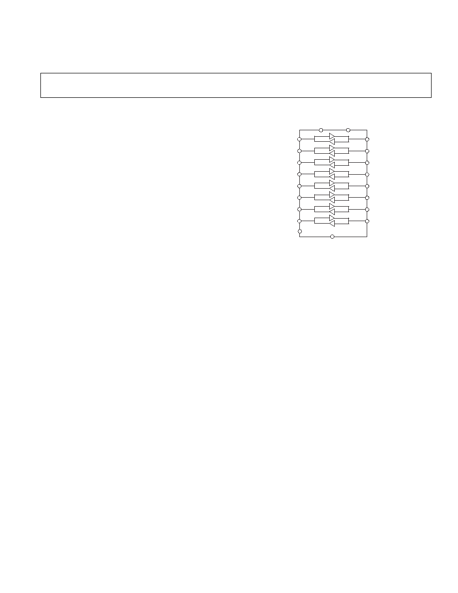
FUNCTIONAL BLOCK DIAGRAM
FEATURES
Bidirectional Level Translation
Operates from 1.2 V to 5.5 V
Low Quiescent Current <5
µµ
µµ
µ
A
APPLICATIONS
SPI
TM
, Microwire
TM
and I
2
C
TM
Translation
Low Voltage ASIC level Translation
Smart Card Readers
Cell Phones & Cell-Phone Cradles
Portable Communication Devices
Telecommunicatons Equipment
Network Switches and Routers
Storage Systems (SAN/NAS)
Computing/Server Applications
GPS
Portable POS Systems
Low Cost Serial Interfaces
GENERAL DESCRIPTION
The ADG3308 is an 8-Channel bidirectional level transla-
tor. Its function is to provide level shifting in a multi-
voltage system. The voltage applied to V
CCA
sets up the
logic levels on the A side of the device, while V
CCY
sets
the levels on the Y side. In this way, signals applied to the
V
CCA
side of the device appear as V
CCY
compatible logic
on the other side of the device and vice versa as the device
is designed to handle bidirectional signals. The device is
guaranteed for operation over the supply range 1.2 V to
5.5 V.
These devices are suited to applications like data transfer
between a low voltage DSP/Controller and a higher
voltage device. Other applications include high end
consumer products where constant changes to the chipset
desgins result in multiple supply levels in the application.
V
CCY
operates from +1.65 to 5.5 V while V
CCA
from +1.2
to V
CCY
. V
CCA
must always operate from a supply that is
lower than V
CCY
. When the device Enable pin (EN) is
pulled low, the Ax and Yx inputs/outputs are tri-stated.
The EN pin is driven high for normal operation. EN pin
is referred to V
CCY
voltage.
PRODUCT HIGHLIGHTS
1.
Bidirectional Level Translation.
2.
The ADG3308 is fully guaranteed from 1.2 V to
5.5 V supply range.
3.
20 lead TSSOP and LFCSP (4mm x4mm) packages.
A1
Y1
GND
VCCY
VCCA
A8
Y8
A7
Y7
A6
Y6
A5
Y5
A4
Y4
A3
Y3
A2
Y2
EN
2
REV. PrE
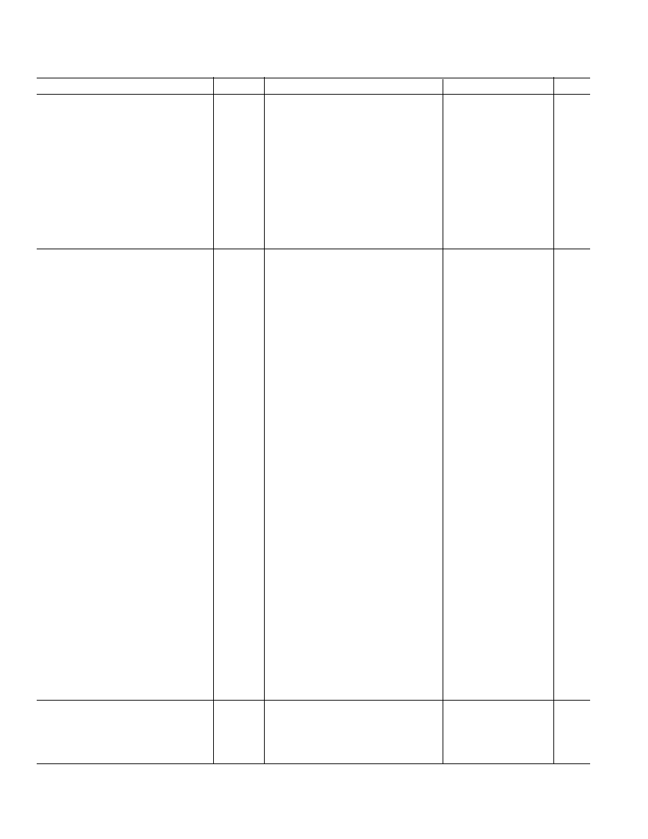
ADG3308SPECIFICATIONS
1
PRELIMINARY TECHNICAL DATA
Parameter
Symbol
Conditions
Min
Typ
2
Max
Units
LOGIC INPUTS/OUTPUTS
Input High Voltage
V
IH
V
CCY
-0.4
V
V
CCA
-0.4
V
Input Low Voltage
V
IL
0.4
V
0.4
V
Output High Voltage
V
OH
I
OH
= 20
µ
A,
V
CCY
-0.4
V
I
OH
= 20
µ
A,
V
CCA
-0.4
V
Output Low Voltage
V
OL
I
OL
= 20
µ
A,
0.4
V
I
OL
= 20
µ
A,
0.4
V
Input Leakage Current
I
I
0 V
IN
3.6 V
±1
µA
Output Leakage Current
I
O
0 V
IN
3.6 V
±1
µA
Input Capacitance
3
C
IN
f = 1 MHz, V
A/Y
= V
CCA/Y
or GND
5
pF
Output Capacitance
3
C
O
f = 1 MHz, V
A/Y
= V
CCY/A
or GND
5
pF
SWITCHING CHARACTERISTICS
3
3.3V ± 0.3V V
CCA
V
CCY
5V ± 0.5V
Propagation Delay,
t
PD
Y - A
R
S
= 50
, C
A
= 15 pF
5
ns
A - Y
R
S
= 50
, C
Y
= 50 pF
5
ns
Rise Time
t
R_Y
R
S
= 50
, C
Y
= 50 pF
5
ns
Fall Time
t
F_Y
R
S
= 50
, C
Y
= 50 pF
5
ns
Rise Time
t
R_A
R
S
= 50
, C
A
= 15 pF
5
ns
Fall Time
t
F_A
R
S
= 50
, C
A
= 15 pF
5
ns
Maximum Data Rate
R
S
= 50
, C
Y
= 50 pF, C
A
= 15 pF
40
Mbps
Channel To Channel Skew
t
SKEW
R
S
= 50
, C
Y
= 50 pF, C
A
= 15 pF
tbd
ns
Part To Part Skew
t
PPSKEW
R
S
= 50
, C
Y
= 50 pF, C
A
= 15 pF
tbd
ns
1.8V ± 0.15V V
CCA
V
CCY
3.3V ±0.3V
Propagation Delay,
t
PD
Y - A
R
S
= 50
, C
A
= 15 pF
10
ns
A - Y
R
S
= 50
, C
Y
= 50 pF
15
ns
Rise Time
t
R_Y
R
S
= 50
, C
Y
= 50 pF
10
ns
Fall Time
t
F_Y
R
S
= 50
, C
Y
= 50 pF
10
ns
Rise Time
t
R_A
R
S
= 50
, C
A
= 15 pF
10
ns
Fall Time
t
F_A
R
S
= 50
, C
A
= 15 pF
10
ns
Maximum Data Rate
R
S
= 50
, C
Y
= 50 pF, C
A
= 15 pF
35
Mbps
Channel To Channel Skew
t
SKEW
R
S
= 50
, C
Y
= 50 pF, C
A
= 15 pF
5
ns
1.2V ± 0.1 V V
CCA
V
CCY
3.3 ± 0.3 V
Propagation Delay,
t
PD
Y - A
R
S
= 50
, C
A
= 15 pF
20
ns
A - Y
R
S
= 50
, C
Y
= 50 pF
20
ns
Rise Time
t
R_Y
R
S
= 50
, C
Y
= 50 pF
15
ns
Fall Time
t
F_Y
R
S
= 50
, C
Y
= 50 pF
15
ns
Rise Time
t
R_A
R
S
= 50
, C
A
= 15 pF
15
ns
Fall Time
t
F_A
R
S
= 50
, C
A
= 15 pF
15
ns
Maximum Data Rate
R
S
= 50
, C
Y
= 50 pF, C
A
= 15 pF
20
Mbps
Channel To Channel Skew
t
SKEW
R
S
= 50
, C
Y
= 50 pF, C
A
= 15 pF
5
ns
2.5V ± 0.2V V
CCA
V
CCY
3.3V ± 0.3V
Propagation Delay,
t
PD
Y - A
R
S
= 50
, C
A
= 15 pF
8.5
ns
A - Y
R
S
= 50
, C
Y
= 50 pF
8.5
ns
Rise Time
t
R_Y
R
S
= 50
, C
Y
= 50 pF
8.5
ns
Fall Time
t
F_Y
R
S
= 50
, C
Y
= 50 pF
8.5
ns
Rise Time
t
R_A
R
S
= 50
, C
A
= 15 pF
8.5
ns
Fall Time
t
F_A
R
S
= 50
, C
A
= 15 pF
8.5
ns
Maximum Data Rate
R
S
= 50
, C
Y
= 50 pF, C
A
= 15 pF
40
Mbps
Channel To Channel Skew
t
SKEW
R
S
= 50
, C
Y
= 50 pF, C
A
= 15 pF
10
ns
POWER REQUIREMENTS
Power Supply Voltages
V
CCY
1.65
5.5
V
V
CCA
1.1
5.5
V
Quiescent Power Supply Current
I
CCY
Digital Inputs = 0 V or V
CCY
5
µA
I
CCA
Digital Inputs = 0 V or V
CCA
5
µA
N O T E S
1
Temperature range is as follows: B Version: 40°C to +85°C.
2
All typical vlaues are at T
A
= +25°C unless otherwise stated.
3
Guaranteed by design, not subject to production test.
Specifications subject to change without notice.
(V
CCY
= +1.65 to 5.5 V, V
CCA
= +1.1 to V
CCY
, GND = 0 V, All specifications T
MIN
to T
MAX
unless otherwise noted)
ADG3308
3
REV. PrE
PRELIMINARY TECHNICAL DATA
ABSOLUTE MAXIMUM RATINGS
1
(T
A
= 25°C unless otherwise noted)
V
CC
Y
to GND . . . . . . . . . . . . . . . . . . . . . . . . . -0.3 V to +7 V
V
CC
A
to GND . . . . . . . . . . . . . . . . . . . . . . . . . -0.3 V to +7 V
Digtal Inputs (A) . . . . . . . . . . . . . . -0.3 V to (V
CC
A
+0.3V)
Digtal Inputs (Y) . . . . . . . . . . . . . . -0.3 V to (V
CC
Y
+0.3V)
EN to GND . . . . . . . . . . . . . . . . . . . . . . . . . -0.3 V to +7 V
Operating Temperature Range
Industrial (B Version) . . . . . . . . . . . . . . 40°C to +85°C
Storage Temperature Range . . . . . . . . . 65°C to +150°C
Junction Temperature . . . . . . . . . . . . . . . . . . . . . . . . 150°C
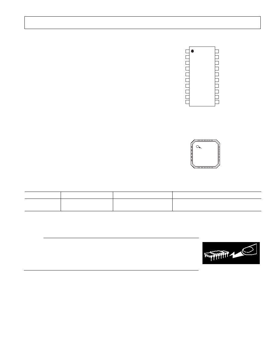
20 Lead TSSOP
JA
Thermal Impedance . . . . . . . . . . . . . . . . . . . . 143°C/W
20 Lead LFCSP - 4 layer board
JA
Thermal Impedance . . . . . . . . . . . . . . . . . . . . . 32°C/W
Lead Temperature, Soldering (10seconds) . . . . . . . 300°C
IR Reflow, Peak Temperature (<20 seconds) . . . +235°C
N O T E S
1
Stresses above those listed under Absolute Maximum Ratings may cause
permanent damage to the device. This is a stress rating only; functional
operation of the device at these or any other conditions above those listed
in the operational sections of this specifcation is not implied. Exposure
to absolute maximum rating conditions for extended periods may affect
device reliability. Only one absolute maximum rating may be applied at
any one time.
C A U T I O N
ESD (electrostatic discharge) sensitive device. Electrostatic charges as high as 4000 V readily
accumulate on the human body and test equipment and can discharge without detection. Although
the ADG3308 features proprietary ESD protection circuitry, permanent damage may
occur on devices subjected to high energy electrostatic discharges. Therefore, proper
ESD precautions are recommended to avoid performance degradation or loss of
functionality.
ORDERING GUIDE
Model
Temperature Range
Package Description
Package Option
ADG3308BRU
40°C to +85°C
T S S O P
RU-20
ADG3308BCP
40°C to +85°C
L F C S P
CP-20
WARNING!
ESD SENSITIVE DEVICE
12 Y8
9
11 GND
10
13 Y7
EN
8
ADG3308
(Not to Scale)
VA
A1
A2
A5
A6
1
2
3
4
5
20
14 Y6
VY
A7
A8
6
7
15
16
17
18
19 Y1
Y2
Y3
Y4
Y5
A3
A4
Pin Configuration
20 Lead TSSOP (RU-20)
20 Lead 4mmx4mm LFCSP
( C P - 2 0 )
PIN 1
INDICATOR
TOP VIEW
ADG3308
1
A2
2
A3
3
A4
4
A5
5
A6
A7 6
A8 7
EN 8
GND 9
Y8 10
15 Y3
14 Y4
13 Y5
12 Y6
11 Y7
20 A1
19 VCCA
18 VCCY
17 Y1
16 Y2
ADG3308
4
REV. PrE
PRELIMINARY TECHNICAL DATA
GENERAL DESCRIPTION
The ADG3308 level translator allows the required level
shifting necessary for data transfer in a system where mul-
tiple voltages are used. The device requires two supplies,
V
CCA
and V
CCY
. These supplies set the logic levels on
each side of the device. The device translates data present
on the V
A
side of the device to the higher voltage level at
the V
Y
side of the device. Similarly, as the device is ca-
pable of bidirectional translation, data applied to the V
Y
side will be translated to the voltage referenced to V
A
.
Power Supplies
The voltage applied to V
CCA
must always be less than or
equal to V
CCY
.
While EN is low, the V
CCA
supply may be removed, and
both A and Y I/O's will remain tri-stated.
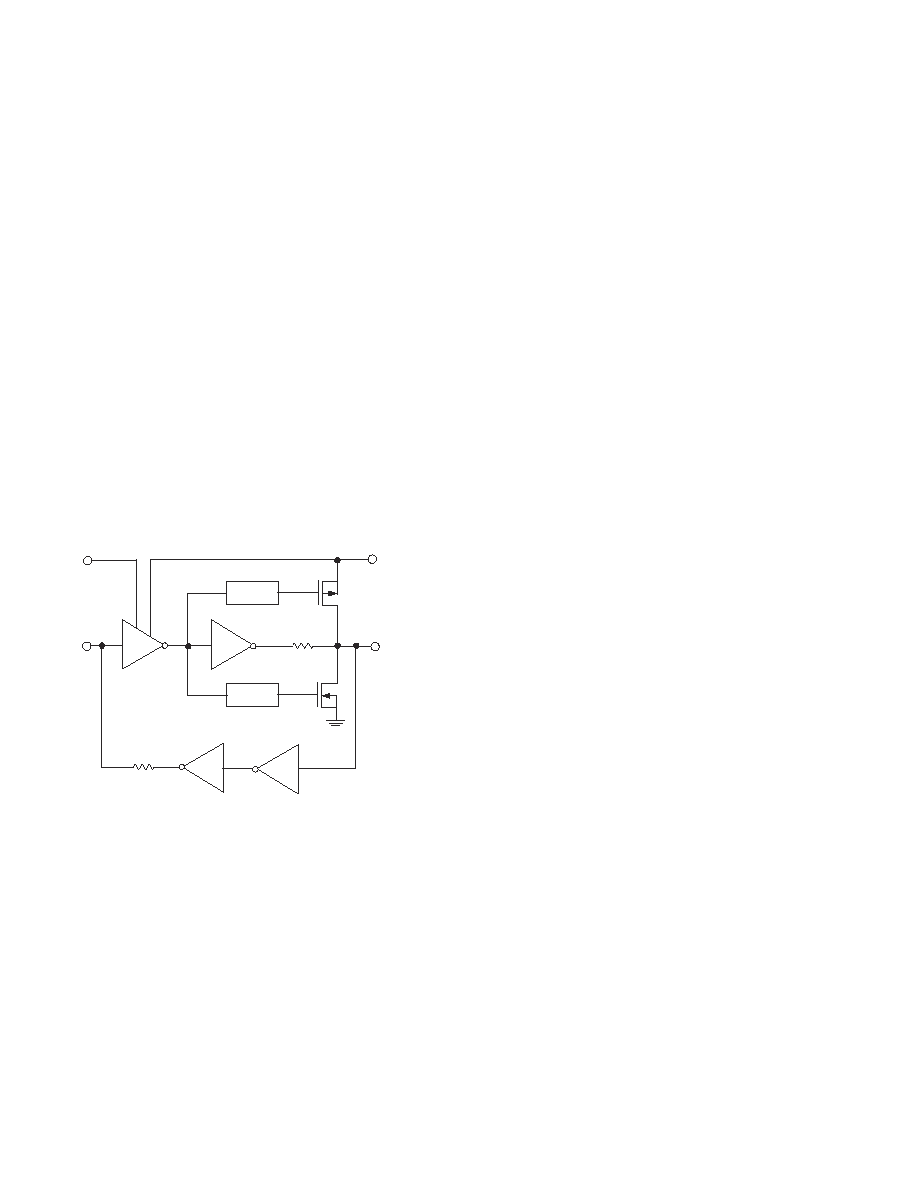
Level Translator Architecture
The forward channel consists of a string of inverters and a
level translator, while the reverse channel consists simply
of inverters. A level translator is not required in the re-
verse path (Y-A) as the supply voltage V
CCY
must always
be greater than or equal to V
CCA
. A current limiting resis-
tor is used in series with each channel to prevent any con-
tention issues, see figure 1.
One Shot
Generator
One Shot
Generator
VCCY
VCCA
A
Y
6k
6k
Figure 1. Simplified Functional Diagram of one channel.
As the driven side has to drive a load capacitance through
this 6k resistance, one shot generators are used to drive
large mos devices in the output stage to help speed up the
rate of switching. The output stage is inactive and three
state except when transistions are present on either side of
the translator. When this happens the one shot fires turn-
ing on the output stage and driving the load capacitance
faster than if it were driven through the resistor. As the
device is bi-directional, both input stages will be active
during this period. While this design gives maximum
speed from the device, it can result in some current driv-
ing back into the source driving the input of the translator.
To ensure correct operation, the input driver should meet
the following requirements - 50
maximum output im-
pedance with minimum of 20mA output current when
driving 20Mbps.
Enable Operation
When pulled low, the EN input allows the user to tri-state
both sides (A and Y) of the level translator. EN pin is
referred to V
CCY
voltage.
ADG3308
5
REV. PrE
PRELIMINARY TECHNICAL DATA
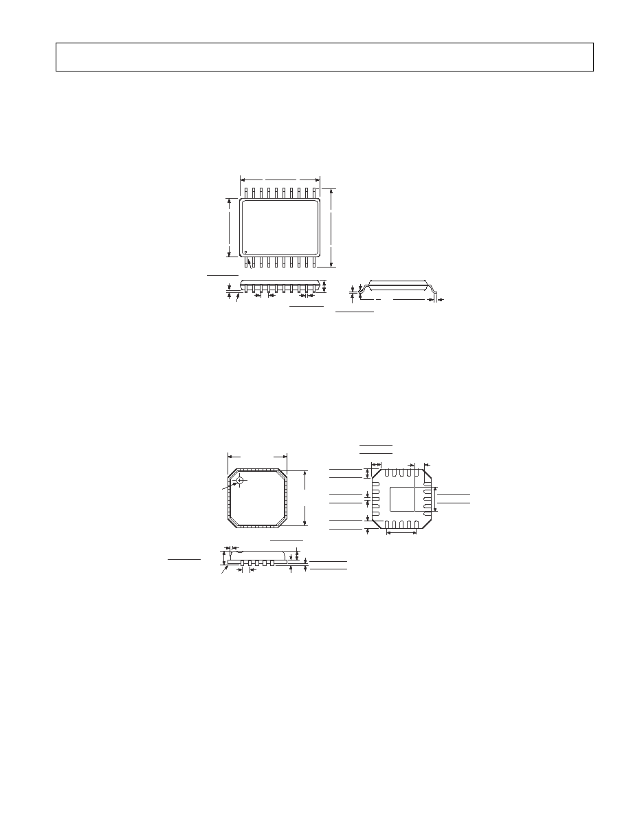
OUTLINE DIMENSIONS
Dimensions shown in inches and (mm).
20-Lead TSSOP
(RU-20)
20
11
10
1
0.260 (6.60)
0.252 (6.40)
0.
256 (
6
.
50)
0.
246 (
6
.
25)
0.
177 (
4
.
50)
0.
169 (
4
.
30)
PIN 1
SEATING
PLANE
0.006 (0.15)
0.002 (0.05)
0.0118 (0.30)
0.0075 (0.19)
0.0256 (0.65)
BSC
0.0433
(1.10)
MAX
0.0079 (0.20)
0.0035 (0.090)
0.028 (0.70)
0.020 (0.50)
8
o
0
o
20-Lead LFCSP
(CP-20)
1
20
5
6
11
16
15
BOTTOM
VIEW
10
0.080 (2.25)
0.083 (2.10) SQ
0.077 (1.95)
0.024 (0.60)
0.017 (0.42)
0.009 (0.24)
0.024 (0.60)
0.017 (0.42)
0.009 (0.24)
0.030 (0.75)
0.024 (0.60)
0.020 (0.50)
0.012 (0.30)
0.009 (0.23)
0.007 (0.18)
0.080 (2.00)
REF
0.010 (0.25)
MIN
0.020 (0.50)
BSC
12
o
MAX
0.008 (0.20)
REF
0.028 (0.70) MAX
0.026 (0.65) NOM
0.002 (0.05)
0.0004 (0.01)
0.0 (0.0)
0.035 (0.90) MAX
0.033 (0.85) NOM
SEATING
PLANE
CONTROLLING DIMENSIONS ARE IN MILLIMETERS
PIN 1
INDICATOR
TOP
VIEW
0.148 (3.75)
BSC SQ
0.157 (4.0)
BSC SQ
PR04865-0-4/04(PrE)