Äîêóìåíòàöèÿ è îïèñàíèÿ www.docs.chipfind.ru
8-Channel CMOS Logic to High Voltage
Level Translator
ADG3123
Rev. A
Information furnished by Analog Devices is believed to be accurate and reliable. However, no
responsibility is assumed by Analog Devices for its use, nor for any infringements of patents or other
rights of third parties that may result from its use. Specifications subject to change without notice. No
license is granted by implication or otherwise under any patent or patent rights of Analog Devices.
Trademarks and registered trademarks are the property of their respective owners.
One Technology Way, P.O. Box 9106, Norwood, MA 02062-9106, U.S.A.
Tel: 781.329.4700
www.analog.com
Fax: 781.461.3113
©2006 Analog Devices, Inc. All rights reserved.
FEATURES
2.3 V to 5.5 V input voltage range
Output voltage levels (V
DDA
and V
DDB
to V
SS
35 V)
Low output voltage levels: down to -24.4 V
High output voltage levels: up to +35 V
Rise/fall time: 12 ns/19.5 ns typical
Propagation delay: 80 ns typical
Operating frequency: 100 kHz typical
Ultralow quiescent current: 65 A typical
20-lead, Pb-free, TSSOP package
APPLICATIONS
Low voltage to high voltage translation
TFT-LCD panels
Piezoelectric motor drivers
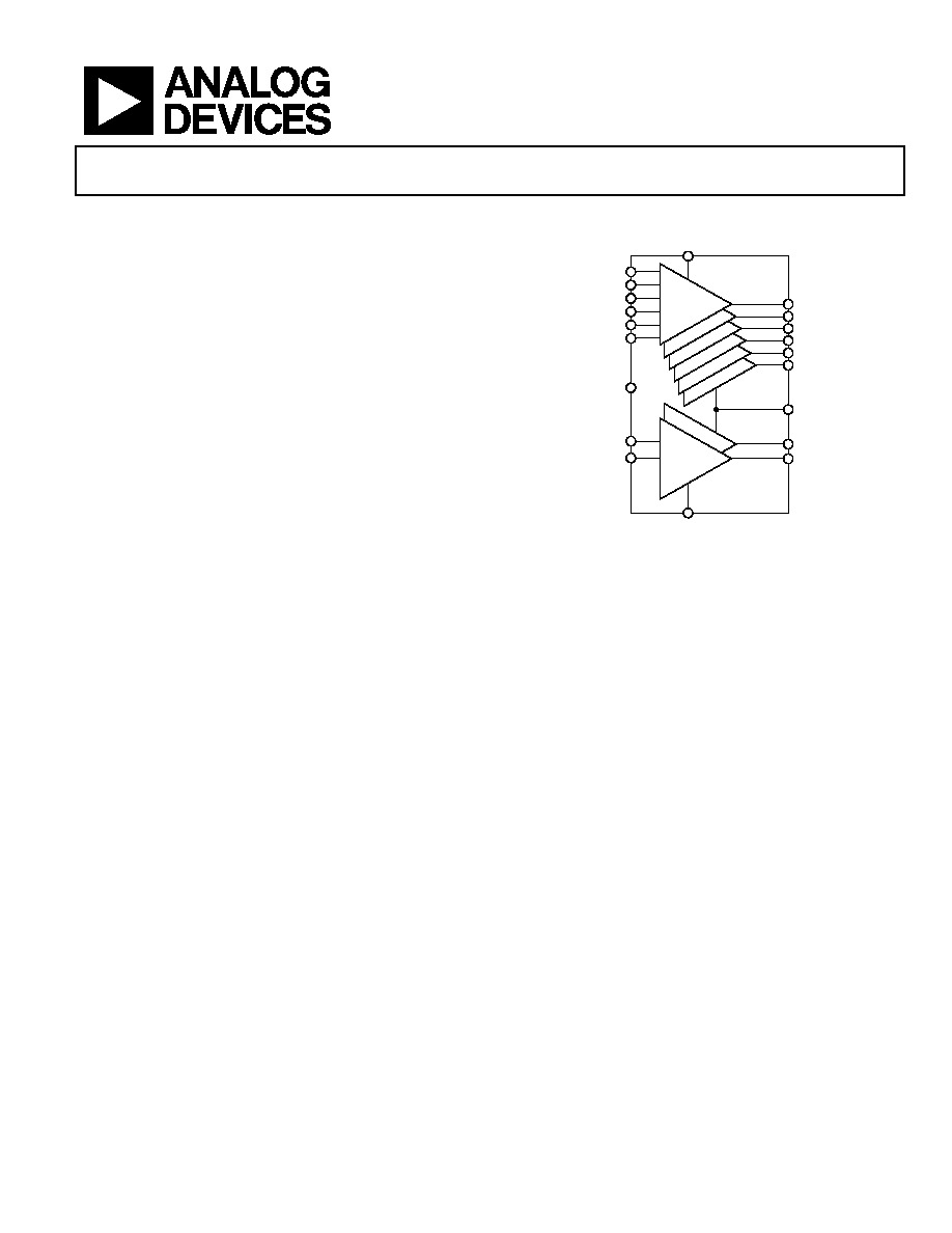
FUNCTIONAL BLOCK DIAGRAM
05
65
5-
0
01
V
DDA
ADG3123
V
DDB
Y6
Y5
Y4
Y3
Y2
Y1
6
CHANNELS
A1
A2
A3
A4
A5
A6
Y8
Y7
V
SS
A7
GND
A8
2
CHANNELS
Figure 1.
GENERAL DESCRIPTION
The ADG3123 is an 8-channel, noninverting CMOS to high
voltage level translator. Fabricated on an enhanced LC
2
MOS
process, the device is capable of operating at high supply
voltages while maintaining ultralow power consumption.
The internal architecture of the device ensures compatibility
with logic circuits running from supply voltages within the 2.3 V to
5.5 V range. The voltages applied to Pin V
DDA
, Pin V
DDB,
and
Pin V
SS
set the logic levels available at the outputs on the Y side
of the device. Pin V
DDA
and Pin V
DDB
set the high output level
for Pin Y1 to Pin Y6 and for Pin Y7 to Pin Y8, respectively. The
V
SS
pin sets the low output level for all channels. The ADG3123
can provide output voltages levels down to -10 V for a low
input level and up to +30 V for a high input logic level. For
proper operation, V
DDB
must always be greater than or equal to
V
DDA
and the voltage between the Pin V
DDB
and Pin V
SS
should
not exceed 35 V.
The low output impedance of the channels guarantees fast rise
and fall times even for significant capacitive loads. This feature,
combined with low propagation delay and low power consump-
tion, makes the ADG3123 an ideal driver for TFT-LCD panel
applications.
The ADG3123 is guaranteed to operate over the -40°C to
+85°C temperature range and is available in a compact, 20-lead
TSSOP, Pb-free package.
PRODUCT HIGHLIGHTS
1.
Compatible with a wide range of CMOS logic levels.
2.
High output voltage levels.
3.
Fast rise and fall times coupled with low propagation delay.
4.
Ultralow power consumption.
5.
Compact, 20-lead TSSOP, Pb-free package.

ADG3123
Rev. A | Page 2 of 12
TABLE OF CONTENTS
Features .............................................................................................. 1
Applications....................................................................................... 1
Functional Block Diagram .............................................................. 1
General Description ......................................................................... 1
Product Highlights ........................................................................... 1
Revision History ............................................................................... 2
Specifications..................................................................................... 3
Absolute Maximum Ratings............................................................ 4
ESD Caution.................................................................................. 4
Pin Configuration and Function Descriptions............................. 5
Typical Performance Characteristics ..............................................6
Terminology .......................................................................................9
Theory of Operation ...................................................................... 10
Input Driving Requirements..................................................... 10
Output Load Requirements ...................................................... 10
Power Supplies ............................................................................ 10
Applications..................................................................................... 11
Outline Dimensions ....................................................................... 12
Ordering Guide .......................................................................... 12
REVISION HISTORY
5/06--Rev. 0 to Rev. A
Changes to Features, General Description, and
Product Highlights ........................................................................... 1
Changes to Specifications ................................................................ 3
Changes to Figure 4 through Figure 9 ........................................... 6
Changes to Figure 14 and Figure 15............................................... 7
Changes to Theory of Operations section and
Power Supplies section................................................................... 10
9/05--Revision 0: Initial Version
ADG3123
Rev. A | Page 3 of 12
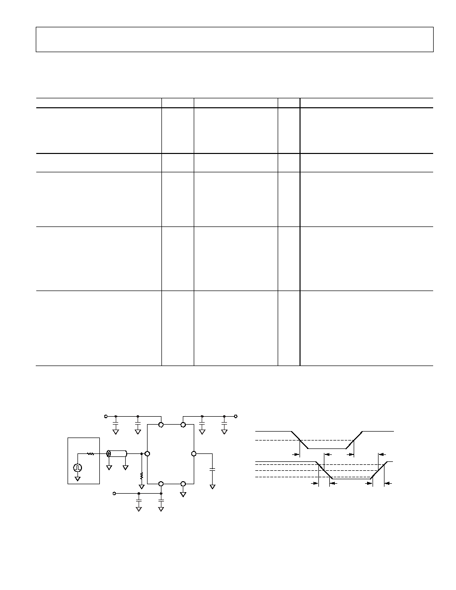
SPECIFICATIONS
V
DDA
= V
DDB
= 27 V, V
SS
= -7 V, GND = 0 V, unless otherwise noted.
1
Table 1.
Parameter
Symbol
Min
Typ
2
Max Unit
Conditions
DIGITAL INPUTS (Pin A1 to Pin A8)
V
AX
= 0 V to 5.5 V
Input High Voltage
V
IH
1.7 V
Input Low Voltage
V
IL
0.8
V
Leakage Current
I
IL
±0.03
±1
A
Capacitance
3
C
I
1
pF
ANALOG INPUTS (Pin V
DDA
)
Input Voltage Range
V
DDA
0
V
DDB
V
DIGITAL OUTPUTS (Pin Y1 to Pin Y8)
V
DDA
= V
DDB
= 25 V to 30 V, V
SS
= -5 V to -7 V,
V
DDA
and V
DDB
to V
SS
35V
Output High Voltage (Pin Y1 to Pin Y6)
V
OH
V
DDA
- 1
V
I
OH
= -10 mA
Output High Voltage (Pin Y7 to Pin Y8)
V
OH
V
DDB
- 1
V
I
OH
= -10 mA
Output Low Voltage
V
OL
V
SS
+ 1
V
I
OL
= +10 mA
Output Impedance
R
0
30
V
DDA
= V
DDB
= +27 V, V
SS
= -7 V
SWITCHING CHARACTERISTICS
3
See
Figure 2
Propagation Delay
Low to High Transition
t
PLH
76
125
ns
High to Low Transition
t
PHL
80
125
ns
Rise Time
t
R
12
20
ns
Fall Time
t
F
19.5
32
ns
Maximum Operating Frequency
F
0
50
100
kHz
100 pF load, all channels, see Figure 2
POWER REQUIREMENTS
Quiescent Power Supply Current
I
DDA
0.03
1 A
V
AX
= 0 V or 5.5 V, no load, V
DDA
V
DDB
I
DDB
65
150
A
I
SS
0.03 1
A
Power Supply Voltages
V
DDB
to V
SS
10.8
35
V
V
DDB
to GND
V
DDB
10.8
35
V
V
DDB
to V
SS
35 V
V
SS
to GND
V
SS
-24.2
0 V
V
DDB
to V
SS
35 V
1
Temperature range for B version is -40°C to +85°C.
2
Typical values are specified at 25°C.
3
Guaranteed by design; not subject to production testing.
05
65
5-
0
02
V
SS
ADG3123
V
DDA
V
DDB
V
SS
GND
A
X
Y
X
V
OUT
V
IN
V
DDB
V
DDA
R
T
50
100pF
10µF
10µF
0.1µF
0.1µF
+
+
Z
0
= 50
R
S
50
SIGNAL
SOURCE
V
IN
50%
90%
50%
10%
V
OUT
t
PHL
t
PLH
t
R
t
F
10µF
0.1µF
+
Figure 2. Switching Characteristics Test Circuit
ADG3123
Rev. A | Page 4 of 12
ABSOLUTE MAXIMUM RATINGS
T
A
= 25°C, unless otherwise noted.
Table 2.
Parameter Rating
V
DDA
/V
DDB
to V
SS
44 V
V
DDB
to GND
-0.3 V to +32 V
V
DDA
to GND
-0.3 V to V
DDB
V
SS
to GND
+0.3 V to -32 V
Digital Inputs
1
V
SS
- 0.3 V to V
DDB
+ 0.3 V or
20 mA, whichever occurs first
Load Current Per Device
Average
15 mA at 25°C
8 mA at 85°C
Peak Current
2
150 mA at 25°C
80 mA at 85°C
Operating Temperature Range
Industrial (B Version)
-40°C to +85°C
Storage Temperature Range
-65°C to +125°C
Junction Temperature
150°C
Thermal Impedance,
JA
78°C/W
3
Reflow Soldering (Pb-Free)
Peak Temperature
260 (+0/-5)°C
Time at Peak Temperature
10 seconds to 40 seconds
1
Overvoltage at Pin A1 to Pin A8 is clamped by internal diodes. Limit the
current to the maximum ratings given.
2
Pulsed at 100 kHz; 10% duty cycle maximum with the load shown in
Figure 2.
3
Guaranteed when the device is soldered on a 4-layer board.
Stresses above those listed under Absolute Maximum Ratings
may cause permanent damage to the device. This is a stress
rating only; functional operation of the device at these or any
other conditions above those indicated in the operational
section of this specification is not implied. Exposure to absolute
maximum rating conditions for extended periods may affect
device reliability.
Only one absolute maximum rating can be applied at any
one time.
ESD CAUTION
ESD (electrostatic discharge) sensitive device. Electrostatic charges as high as 4000 V readily accumulate on
the human body and test equipment and can discharge without detection. Although this product features
proprietary ESD protection circuitry, permanent damage may occur on devices subjected to high energy
electrostatic discharges. Therefore, proper ESD precautions are recommended to avoid performance
degradation or loss of functionality.
ADG3123
Rev. A | Page 5 of 12
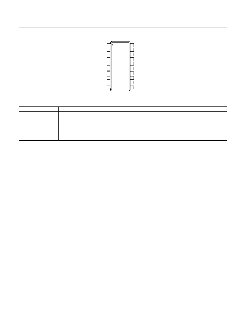
PIN CONFIGURATION AND FUNCTION DESCRIPTIONS
05
65
5-
0
03
1
2
3
4
5
6
7
8
9
10
20
19
18
17
16
15
14
13
12
11
A1
A2
A3
A6
A5
A4
GND
Y1
Y2
Y3
Y6
Y5
Y4
V
SS
A8
A7
V
DDB
Y8
Y7
V
DDA
ADG3123
TOP VIEW
(Not to Scale)
Figure 3. Pin Configuration
Table 3. Pin Function Descriptions
Pin No.
Mnemonic
Description
1 GND Ground
Reference
(0
V).
2 to 9
A1 to A8
Level Translator CMOS Inputs.
10 V
SS
Most Negative Power Supply. Use the V
SS
pin to generate the output low level for Output Y1 to Output Y8.
11 V
DDB
Positive Power Supply. Use the V
DDB
pin to generate the output high level for Output Y7 and Output Y8.
12 to 19
Y8 to Y1
Level Translator High Voltage Outputs.
20 V
DDA
Analog Input. Use the V
DDA
pin to generate the output high level for Output Y1 to Output Y6 (V
DDA
V
DDB
).
ADG3123
Rev. A | Page 6 of 12
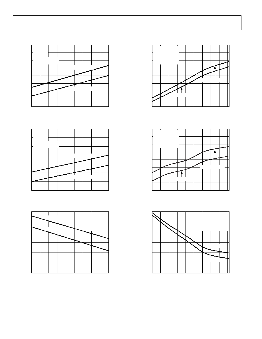
TYPICAL PERFORMANCE CHARACTERISTICS
4.1
2.5
10
100
FREQUENCY (kHz)
I
DD
B
(m
A
)
3.9
3.7
3.5
3.3
3.1
2.9
2.7
20
30
40
50
60
70
80
90
V
DDA
= V
DDB
= 27V
V
DDA
= V
DDB
= 25V
T
A
= 25°C
V
SS
= 7V
R
L
= 5k
C
L
= 100pF
DUTY CYCLE = 50%
1 CHANNEL
05
65
5-
00
4
Figure 4. Supply Current (I
DDB
) vs. Frequency
3.9
2.5
10
100
FREQUENCY (kHz)
I
DD
A
(m
A
)
20
30
40
50
60
70
80
90
3.7
3.5
3.3
3.1
2.9
2.7
T
A
= 25°C
V
SS
= 7V
R
L
= 5k
C
L
= 100pF
DUTY CYCLE = 50%
1 CHANNEL
V
DDA
= V
DDB
= 27V
V
DDA
= V
DDB
= 25V
05
65
5-
00
5
Figure 5. Supply Current (I
DDA
) vs. Frequency
0.5
1.7
10
100
FREQUENCY (kHz)
I
SS
(m
A
)
20
30
40
50
60
70
80
90
V
SS
= 5V
V
SS
= 7V
0.7
0.9
1.1
1.3
1.5
T
A
= 25°C
V
DDA
= V
DDB
= 27V
R
L
= 5k
C
L
= 100pF
DUTY CYCLE = 50%
1 CHANNEL
05
65
5-
00
6
Figure 6. Supply Current (I
SS
) vs. Frequency
6.5
2.5
0.1
4.6
4.1
3.6
3.1
2.6
2.1
1.6
1.1
0.6
CAPACITIVE LOAD (nF)
I
DD
B
(m
A
)
4.5
6.0
5.5
5.0
4.0
3.5
3.0
V
DDA
= V
DDB
= 27V
V
DDA
= V
DDB
= 25V
T
A
= 25°C
V
SS
= 7V
R
L
= 5k
FREQUENCY = 20kHz
DUTY CYCLE = 50%
1 CHANNEL
05
65
5-
00
7
Figure 7. Supply Current (I
DDB
) vs. Capacitive Load
4.1
2.5
0.1
4.6
4.1
3.6
3.1
2.6
2.1
1.6
1.1
0.6
CAPACITIVE LOAD (nF)
I
DD
A
(m
A
)
3.3
3.9
3.7
3.5
3.1
2.9
2.7
V
DDA
= V
DDB
= 27V
V
DDA
= V
DDB
= 25V
T
A
= 25°C
V
SS
= 7V
R
L
= 5k
FREQUENCY = 20kHz
DUTY CYCLE = 50%
1 CHANNEL
05
65
5-
00
8
Figure 8. Supply Current (I
DDA
) vs. Capacitive Load
0.5
6.5
5.5
4.5
3.5
2.5
1.5
0.1
4.6
4.1
3.6
3.1
2.6
2.1
1.6
1.1
0.6
CAPACITIVE LOAD (nF)
I
SS
(m
A
)
V
SS
= 5V
V
SS
= 7V
T
A
= 25°C
V
DDA
= V
DDB
= 27V
R
L
= 5k
FREQUENCY = 20kHz
DUTY CYCLE = 50%
1 CHANNEL
05
65
5-
00
9
Figure 9. Supply Current (I
SS
) vs. Capacitive Load
ADG3123
Rev. A | Page 7 of 12
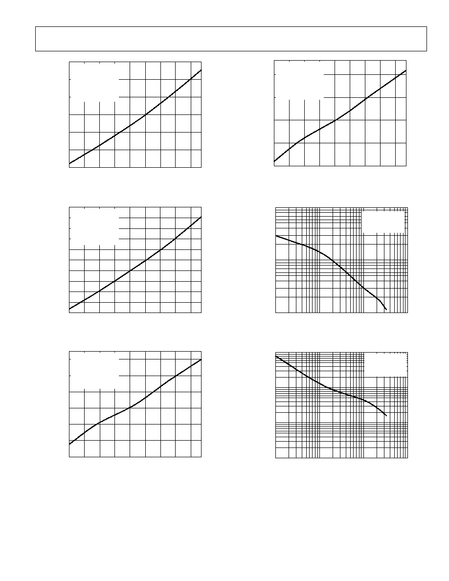
300
0
0.10
CAPACITIVE LOAD (nF)
RI
S
E
T
I
M
E
(
n
s)
250
200
150
100
50
0.60
1.10
1.60
2.10
2.60
3.10
3.60
4.10
T
A
= 25°C
V
DDA
= V
DDB
= 27V
V
SS
= 7V
R
L
= 5k
FREQUENCY = 20kHz
DUTY CYCLE = 50%
1 CHANNEL
05
65
5-
01
0
Figure 10. Rise Time vs. Capacitive Load
500
300
350
400
450
0
0.10
CAPACITIVE LOAD (nF)
F
A
LL
TIM
E
(ns
)
250
200
150
100
50
0.60
1.10
1.60
2.10
2.60
3.10
3.60
4.10
T
A
= 25°C
V
DDA
= V
DDB
= 27V
V
SS
= 7V
R
L
= 5k
FREQUENCY = 20kHz
DUTY CYCLE = 50%
1 CHANNEL
05
65
5-
0
1
1
Figure 11. Fall Time vs. Capacitive Load
140
160
180
60
0.10
CAPACITIVE LOAD (nF)
t
PL
H
(n
s)
120
100
80
0.60
1.10
1.60
2.10
2.60
3.10
3.60
4.10
T
A
= 25°C
V
DDA
= V
DDB
= 27V
V
SS
= 7V
R
L
= 5k
FREQUENCY = 20kHz
DUTY CYCLE = 50%
1 CHANNEL
05
65
5-
01
2
Figure 12. Propagation Delay (t
PLH
) vs. Capacitive Load
220
270
70
0.10
CAPACITIVE LOAD (nF)
t
PL
H
(n
s)
170
120
0.60
1.10
1.60
2.10
2.60
3.10
3.60
4.10
T
A
= 25°C
V
DDA
= V
DDB
= 27V
V
SS
= 7V
R
L
= 5k
FREQUENCY = 20kHz
DUTY CYCLE = 50%
1 CHANNEL
05
65
5-
01
3
Figure 13. Propagation Delay (t
PHL
) vs. Capacitive Load
10
1
0.1
0.01
0.1
1
10
05
65
5-
01
4
F
RE
Q
UE
NCY
(
M
Hz
)
CAPACITIVE LOAD (nF)
V
DDA
= V
DDB
= 27V
V
SS
= 7V
T
A
= 250°C
1 CHANNEL
Figure 14. Maximum Operating Frequency vs. Capacitive Load
(One Channel)
1000
10
100
1
0.01
0.1
1
10
05
65
5-
0
15
F
RE
Q
U
E
NCY
(
k
Hz
)
CAPACITIVE LOAD (nF)
V
DDA
= V
DDB
= 27V
V
SS
= 7V
T
A
= 25°C
8 CHANNELS
Figure 15. Maximum Operating Frequency vs. Capacitive Load
(Eight Channels)
ADG3123
Rev. A | Page 8 of 12
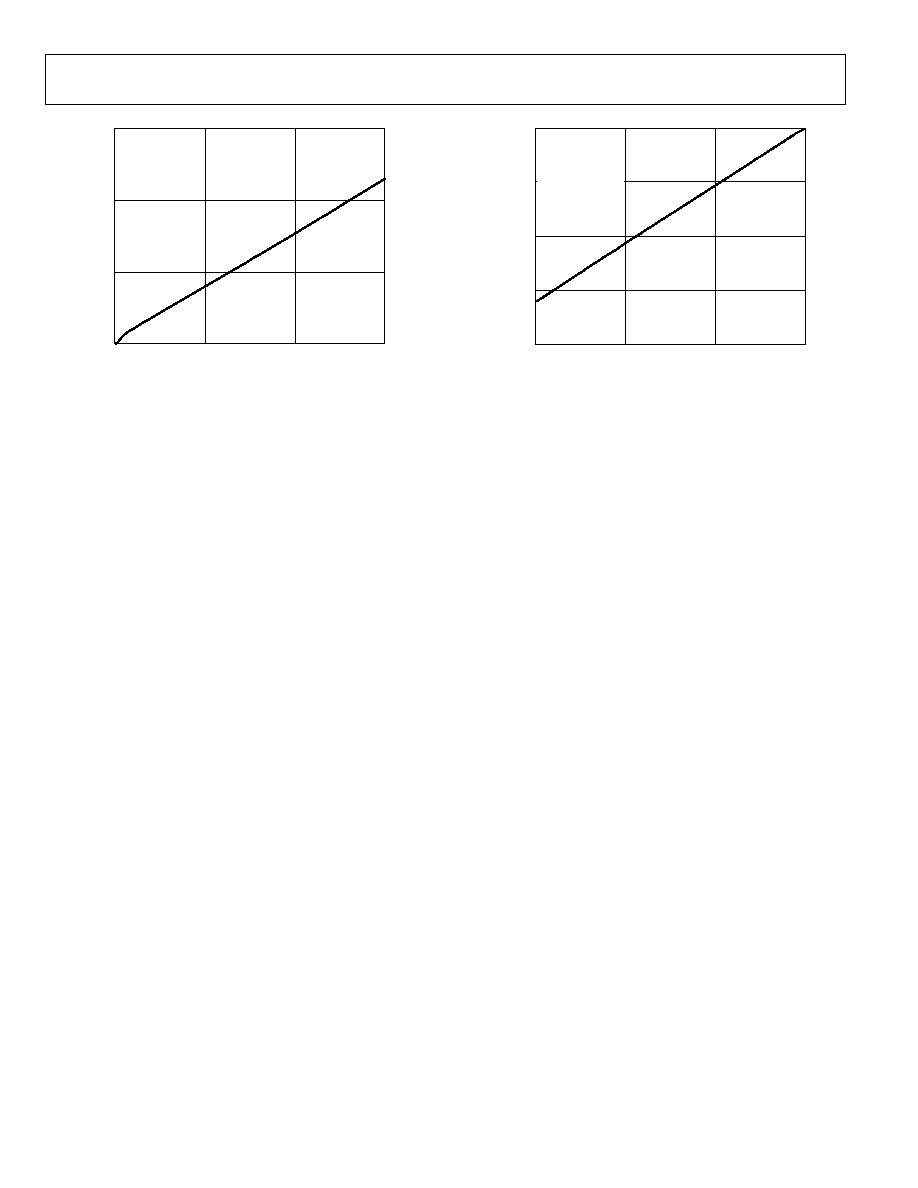
6.4
7.0
0
15
LOAD CURRENT (mA)
V
OL
(V
)
6.6
6.8
5
10
T
A
= 25
°C
V
DDA
= V
DDB
= 27V
V
SS
= 7V
1 CHANNEL
V
AX
= 0V
05655-014
Figure 16. Output Voltage (V
OL
) vs. Load Current
27.0
26.6
15
0
LOAD CURRENT (mA)
V
OH
(V
)
26.9
26.8
26.7
10
5
T
A
= 25
°C
V
DDA
= V
DDB
= 27V
V
SS
= 7V
1 CHANNEL
V
AX
= 5.5V
05655-015
Figure 17. Output Voltage (V
OH
) vs. Load Current

ADG3123
Rev. A | Page 9 of 12
TERMINOLOGY
V
IH
Logic input high voltage at Pin A1 to Pin A8.
V
IL
Logic input low voltage at Pin A1 to Pin A8.
I
IL
Leakage current at Pin A1 to Pin A8.
C
I
Capacitance measured at Pin A1 to Pin A8.
V
O
H
Logic output high voltage at Pin Y1 to Pin Y8.
V
OL
Logic output low voltage at Pin Y1 to Pin Y8.
Ro
Output impedance.
t
PLH
Propagation delay through the part measured between the input
signal applied to any one channel and its corresponding output
for a low-to-high transition (see Figure 2).
t
PHL
Propagation delay through the part measured between the input
signal applied to any one channel and its corresponding output
for a high-to-low transition (see Figure 2).
t
R
Rise time of the output signal at Pin Y1 to Pin Y8 (see Figure 2).
t
F
Fall time of the output signal at the Pin Y1 to Pin Y8
(see Figure 2).
F
O
Frequency of the signal applied to the A1 to A8 input pins.
V
DDA
Input voltage used to generate the high logic levels for Y1 to Y6
outputs.
V
DDB
Positive power supply voltage. Also used to generate the high
logic levels for Y7 to Y8 outputs.
V
SS
Negative power supply voltage. It is used to generate the low
logic level for Y1 to Y8 outputs.
GND
Ground (0 V) reference.
I
DDA
Supply current at the V
DDA
pin.
I
DDB
Supply current at the V
DDB
pin.
I
SS
Supply current at the V
SS
pin.

ADG3123
Rev. A | Page 10 of 12
THEORY OF OPERATION
The ADG3123 is an 8-channel, noninverting CMOS to high
voltage level translator. Fabricated on an enhanced LC
2
MOS
process, the device is capable of operating at high supply
voltages while maintaining ultralow power consumption.
The device requires a dual-supply voltage, V
DDB
and V
SS
, which
sets the low logic levels for all outputs and the high logic levels
for the Y7 and Y8 outputs. The V
DDA
pin acts as an analog input.
The voltage applied to the V
DDA
pin sets the output high logic
level for the Y1 to Y6 outputs.
The device translates the CMOS logic levels applied to the A1 to
A8 inputs into high voltage bipolar levels available on the Y side
of the device at Pin Y1 to Pin Y8.
To ensure proper operation, V
DDB
must always be greater than
or equal to V
DDA
and the voltage between the Pin V
DDB
and
Pin V
SS
should not exceed 35 V.
INPUT DRIVING REQUIREMENTS
The ADG3123 design ensures low input capacitance and
leakage current thereby reducing the loading of the circuit that
drives the input pins (Pin A1 to Pin A8) to a minimum. Its
input threshold levels are compliant with JEDEC standards for
drivers operated from supply voltages between 2.3 V and 5.5 V.
It is recommended that the inputs of any unused channel be
tied to a stable logic level (low or high).
OUTPUT LOAD REQUIREMENTS
The low output impedance of the ADG3123 allows each
channel to drive both resistive and capacitive loads. The
maximum load current is limited by the current carrying
capability of any given channel. If more channels are used, the
maximum load current per channel is reduced accordingly.
Note that the sum of the load currents on all channels should
never exceed the absolute maximum ratings specifications.
The average load current on each channel, I
CHANNEL
, can be
determined using the formulas shown in the Capacitive Loads
and the Resistive Loads sections.
Capacitive Loads
|)
|
(
)
(
SS
DDX
L
O
CHANNEL
V
V
C
F
A
I
+
×
×
=
where:
F
O
is the frequency of the signal applied to the channel in Hz.
C
L
is the load capacitance in farads.
V
SS
is the voltage applied to the V
SS
pin.
V
DDX
is V
DDA
for Y1 to Y6 outputs, and V
DDB
for Y7 to Y8
outputs.
Resistive Loads
L
SS
DDX
CHANNEL
R
V
D
V
D
A
I
×
-
+
×
=
)
1
(
)
(
where:
D
is the duty cycle of the input signal. D is defined as the ratio
between the high state duration of the signal and its period.
R
L
is the load resistor in .
V
SS
is the voltage applied to the V
SS
pin.
V
DDX
is V
DDA
for Y1 to Y6 outputs, and V
DDB
for Y7 to Y8
outputs.
POWER SUPPLIES
The ADG3123 operates from a dual-supply voltage. As good
design practice for all CMOS devices dictates, power up the
ADG3123 first (V
DDB
and V
SS
) before applying the signals to its
inputs (A1 to A8 and V
DDA
). To ensure correct operation of the
ADG3123, the voltage applied to the V
DDB
pin must always be
greater than or equal to V
DDA
and the voltage between the
Pin V
DDB
and Pin V
SS
should not exceed 35 V.
To ensure optimum performance, use decoupling capacitors on
all power supply pins. Furthermore, good engineering and
layout practice suggests placing these capacitors as close as
possible to the package supply pins.
ADG3123
Rev. A | Page 11 of 12
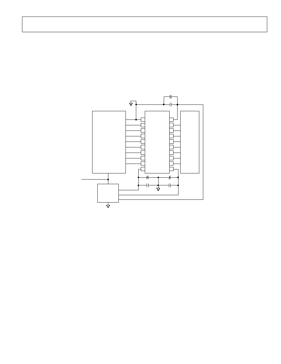
APPLICATIONS
The high voltage operation coupled with high current driving
capability and the wide range of CMOS levels accepted by the
ADG3123, make the device ideal for LCD-TFT panel applica-
tions. In this type of application, the controllers that generate
the timing signals required to control the pixel scanning process
inside the panel are usually low voltage CMOS devices.
Most LCD-TFT panels operate at high supply voltages; therefore,
the timing signals generated by the controller require level
translation to drive the panel. Figure 18 shows a typical applica-
tion circuit where the ADG3123 translates eight timing signals
provided by the timing controller into high voltage logic levels
required to drive the panel.
0
56
55
-
0
16
1
2
3
4
5
6
7
8
9
10
20
19
18
17
16
15
14
13
12
11
Y1
Y2
Y3
Y6
Y5
Y4
V
DDB
Y8
Y7
V
DDA
A1
A2
A3
A6
A5
A4
GND
V
SS
A8
A7
ADG3123
LCD-TFT
PANEL
OUT1
OUT2
OUT3
OUT6
OUT5
OUT4
GND
OUT8
OUT7
TIMING
CONTROLLER
V
DD
10µF
10µF
0.1µF
0.1µF
V
DD
= +2.3V TO +5.5V
DC TO DC
CONVERTER
5V TO 10V
+25V TO +30V
+25V TO +30V
+
+
10µF
+
0.1µF
NOTE: |V
DDB
| + |V
SS
| 35V and V
DDA
V
DDB
Figure 18. Typical Application Circuit
ADG3123
Rev. A | Page 12 of 12
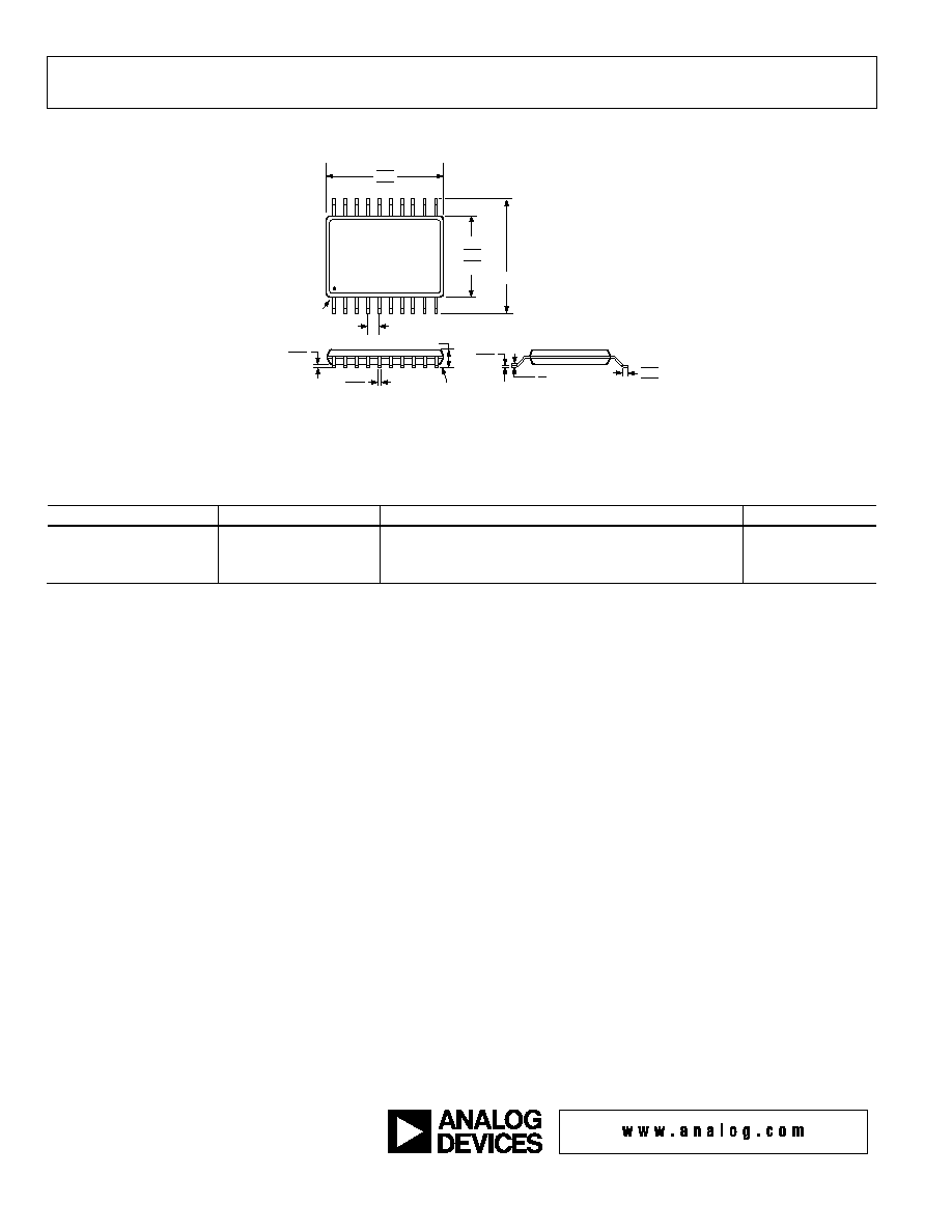
OUTLINE DIMENSIONS
COMPLIANT TO JEDEC STANDARDS MO-153-AC
20
1
11
10
6.40 BSC
4.50
4.40
4.30
PIN 1
6.60
6.50
6.40
SEATING
PLANE
0.15
0.05
0.30
0.19
0.65
BSC
1.20 MAX
0.20
0.09
0.75
0.60
0.45
8°
0°
COPLANARITY
0.10
Figure 19. 20-Lead Thin Shrink Small Outline Package [TSSOP]
(RU-20)
Dimensions shown in millimeters
ORDERING GUIDE
Model
Temperature Range
Package Description
Package Option
ADG3123BRUZ
1
-40°C to +85°C
20-Lead Thin Shrink Small Outline Package (TSSOP)
RU-20
ADG3123BRUZ-REEL
1
-40°C to +85°C
20-Lead Thin Shrink Small Outline Package (TSSOP)
RU-20
ADG3123BRUZ-REEL7
1
-40°C to +85°C
20-Lead Thin Shrink Small Outline Package (TSSOP)
RU-20
1
Z = Pb-free part.
©2006 Analog Devices, Inc. All rights reserved. Trademarks and
registered trademarks are the property of their respective owners.
D05655-0-5/06(A)
Document Outline
- þÿ
- þÿ
- þÿ
- þÿ
- þÿ
- TABLE OF CONTENTS
- þÿ
- SPECIFICATIONS
- þÿ
- þÿ
- þÿ
- þÿ
- þÿ
- þÿ
- þÿ