Äîêóìåíòàöèÿ è îïèñàíèÿ www.docs.chipfind.ru
REV. 0
Information furnished by Analog Devices is believed to be accurate and
reliable. However, no responsibility is assumed by Analog Devices for its
use, nor for any infringements of patents or other rights of third parties
which may result from its use. No license is granted by implication or
otherwise under any patent or patent rights of Analog Devices.
a
ADF4116/ADF4117/ADF4118
One Technology Way, P.O. Box 9106, Norwood, MA 02062-9106, U.S.A.
Tel: 781/329-4700
World Wide Web Site: http://www.analog.com
Fax: 781/326-8703
© Analog Devices, Inc., 2000
RF PLL Frequency Synthesizers
FEATURES
ADF4116: 550 MHz
ADF4117: 1.2 GHz
ADF4118: 3.0 GHz
2.7 V to 5.5 V Power Supply
Separate V
P
Allows Extended Tuning Voltage in 3 V
Systems
Selected Charge Pump Currents
Dual Modulus Prescaler
ADF4116: 8/9
ADF4117/ADF4118: 32/33
3-Wire Serial Interface
Digital Lock Detect
Power-Down Mode
Fast Lock Mode
APPLICATIONS
Base Stations for Wireless Radio (GSM, PCS, DCS,
CDMA, WCDMA)
Wireless Handsets (GSM, PCS, DCS, CDMA, WCDMA)
Wireless LANS
Communications Test Equipment
CATV Equipment
GENERAL DESCRIPTION
The ADF4116 family of frequency synthesizers can be used
to implement local oscillators in the up-conversion and down-
conversion sections of wireless receivers and transmitters. They
consist of a low-noise digital PFD (Phase Frequency Detector),
a precision charge pump, a programmable reference divider,
programmable A and B counters and a dual-modulus prescaler
(P/P+1). The A (5-bit) and B (13-bit) counters, in conjunction
with the dual modulus prescaler (P/P+1), implement an N
divider (N = BP+A). In addition, the 14-bit reference counter
(R Counter), allows selectable REFIN frequencies at the PFD
input. A complete PLL (Phase-Locked Loop) can be imple-
mented if the synthesizer is used with an external loop filter and
VCO (Voltage Controlled Oscillator).
Control of all the on-chip registers is via a simple 3-wire interface.
The devices operate with a power supply ranging from 2.7 V to
5.5 V and can be powered down when not in use.
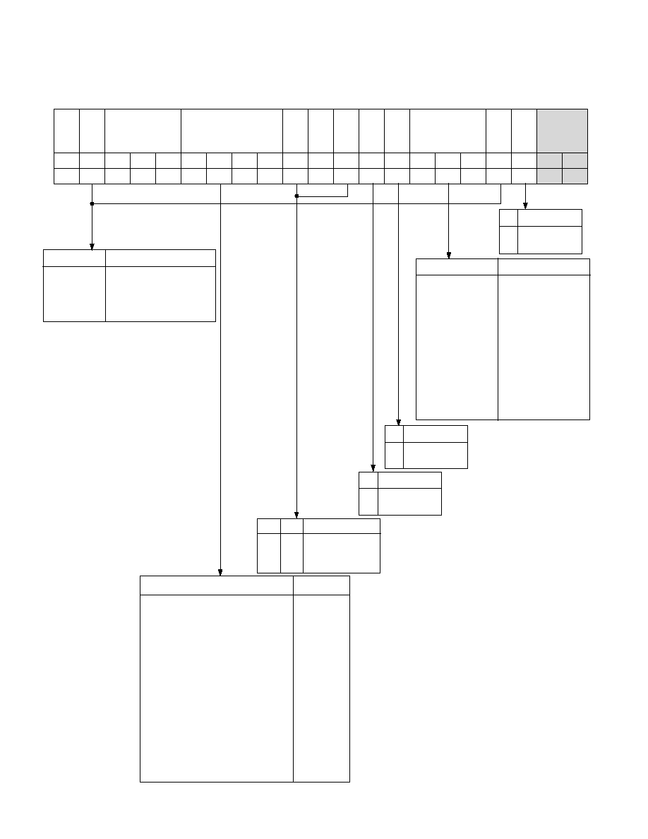
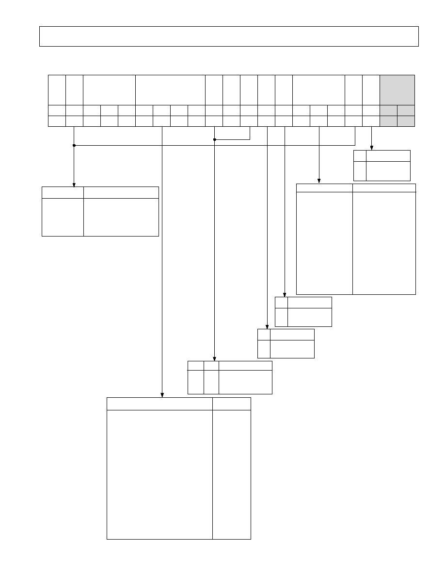
FUNCTIONAL BLOCK DIAGRAM
REFERENCE
FL
O
SWITCH
N = BP + A
FUNCTION
LATCH
PRESCALER
P/P +1
13-BIT
B COUNTER
5-BIT
A COUNTER
14-BIT
R COUNTER
21-BIT
INPUT REGISTER
R COUNTER
LATCH
A, B COUNTER
LATCH
PHASE
FREQUENCY
DETECTOR
CHARGE
PUMP
M3
M2
M1
HIGH Z
MUX
MUXOUT
CP
FL
O
AV
DD
SD
OUT
18
13
14
19
SD
OUT
FROM
FUNCTION LATCH
5
DGND
AGND
CE
RF
IN
B
RF
IN
A
LE
DATA
CLK
REF
IN
CPGND
V
P
DV
DD
AV
DD
LOCK
DETECT
ADF4116/ADF4117/ADF4118
LOAD
LOAD

2
REV. 0
ADF4116/ADF4117/ADF4118SPECIFICATIONS
1
(AV
DD
= DV
DD
= 3 V 10%, 5 V 10%; AV
DD
V
P
6.0 V; AGND = DGND = CPGND = 0 V; T
A
= T
MIN
to T
MAX
unless otherwise noted)
Parameter
B Version
B Chips
2
Unit
Test Conditions/Comments
RF CHARACTERISTICS
RF Input Frequency
See Figure 22 for Input Circuit
ADF4116
45/550
45/550
MHz min/max
ADF4117
0.045/1.2
0.045/1.2
GHz min/max
ADF4118
0.1/3.0
0.1/3.0
GHz min/max
Input Level = 10 dBm
ADF4118
0.2/3.0
0.2/3.0
GHz min/max
Maximum Allowable
Prescaler Output Frequency
3
165
165
MHz max
AV
DD,
DV
DD
= 3 V
200
200
MHz max
AV
DD,
DV
DD
= 5 V
RF Input Sensitivity
15/0
15/0
dBm min/max
AV
DD
= 3 V
10/0
10/0
dBm min/max
AV
DD
= 5 V
REFIN CHARACTERISTICS
Reference Input Frequency
0/100
0/100
MHz min/max
Reference Input Sensitivity
4
5/0
5/0
dBm min/max
AC-Coupled. When DC-Coupled:
0 to V
DD
Max (CMOS Compatible)
REFIN Input Capacitance
10
10
pF max
REFIN Input Current
±100
±100
µA max
PHASE DETECTOR FREQUENCY
5
55
55
MHz max
CHARGE PUMP
I
CP
Sink/Source
High Value
1
1
mA typ
Low Value
250
250
µA typ
Absolute Accuracy
2.5
2.5
% typ
I
CP
Three-State Leakage Current
1
1
nA max
Sink and Source Current Matching
3
3
% typ
0.5 V
V
CP
V
P
0.5
I
CP
vs. V
CP
2
2
% typ
0.5 V
V
CP
V
P
0.5
I
CP
vs. Temperature
2
2
% typ
V
CP
= V
P
/2
LOGIC INPUTS
V
INH
, Input High Voltage
0.8
× DV
DD
0.8
× DV
DD
V min
V
INL
, Input Low Voltage
0.2
× DV
DD
0.2
× DV
DD
V max
I
INH
/I
INL
, Input Current
±1
±1
µA max
C
IN
, Input Capacitance
10
10
pF max
Reference Input Current
±100
±100
µA max
LOGIC OUTPUTS
V
OH
, Output High Voltage
DV
DD
0.4
DV
DD
0.4
V min
I
OH
= 500
µA
V
OL
, Output Low Voltage
0.4
0.4
V max
I
OL
= 500
µA
POWER SUPPLIES
AV
DD
2.7/5.5
2.7/5.5
V min/V max
DV
DD
AV
DD
AV
DD
V
P
AV
DD
/6.0
AV
DD
/6.0
V min/V max
AV
DD
V
P
6.0 V
I
DD
6
(AI
DD
+ DI
DD
)
See Figure 20
ADF4116
5.5
4.5
mA max
4.5 mA Typical
ADF4117
5.5
4.5
mA max
4.5 mA Typical
ADF4118
7.5
6.5
mA max
6.5 mA Typical
I
P
0.4
0.4
mA max
T
A
= 25
°C
Low-Power Sleep Mode
1
1
µA typ
3
REV. 0
ADF4116/ADF4117/ADF4118
Parameter
B Version
B Chips
2
Unit
Test Conditions/Comments
NOISE CHARACTERISTICS
ADF4118 Phase Noise Floor
7
170
170
dBc/Hz typ
@ 25 kHz PFD Frequency
162
162
dBc/Hz typ
@ 200 kHz PFD Frequency
Phase Noise Performance
8
@ VCO Output
ADF4116
9
540 MHz Output
89
89
dBc/Hz typ
@ 1 kHz Offset and 200 kHz PFD Frequency
ADF4117
10
900 MHz Output
87
87
dBc/Hz typ
Note 15
ADF4118
10
900 MHz Output
90
90
dBc/Hz typ
Note 15
ADF4117
11
836 MHz Output
78
78
dBc/Hz typ
@ 300 Hz Offset and 30 kHz PFD Frequency
ADF4118
12
1750 MHz Output
85
85
dBc/Hz typ
@ 1 kHz Offset and 200 kHz PFD Frequency
ADF4118
13
1750 MHz Output
65
65
dBc/Hz typ
@ 200 Hz Offset and 10 kHz PFD Frequency
ADF4118
14
1960 MHz Output
84
84
dBc/Hz typ
@ 1 kHz Offset and 200 kHz PFD Frequency
Spurious Signals
ADF4116
9
540 MHz Output
88/99
88/99
dBc typ
@ 200 kHz/400 kHz and 200 kHz PFD Frequency
ADF4117
10
900 MHz Output
90/104
90/104
dBc typ
Note 15
ADF4118
10
900 MHz Output
91/100
91/100
dBc typ
Note 15
ADF4117
11
836 MHz Output
80/84
80/84
dBc typ
@ 30 kHz/60 kHz and 30 kHz PFD Frequency
ADF4118
12
1750 MHz Output
88/90
88/90
dBc typ
@ 200 kHz/400 kHz and 200 kHz PFD Frequency
ADF4118
13
1750 MHz Output
65/73
65/73
dBc typ
@ 10 kHz/20 kHz and 10 kHz PFD Frequency
ADF4118
14
1960 MHz Output
80/86
80/86
dBc typ
@ 200 kHz/400 kHz and 200 kHz PFD Frequency
NOTES
1
Operating temperature range is as follows: B Version: 40
°C to +85°C.
2
The B Chip specifications are given as typical values.
3
This is the maximum operating frequency of the CMOS counters.
4
AV
DD
= DV
DD
= 3 V; for AV
DD
= DV
DD
= 5 V, use CMOS-compatible levels.
5
Guaranteed by design. Sample tested to ensure compliance.
6
AV
DD
= DV
DD
= 3 V; RF
IN
for ADF4116 = 540 MHz; RF
IN
for ADF4117, ADF4118 = 900 MHz.
7
The synthesizer phase noise floor is estimated by measuring the in-band phase noise at the output of the VCO and subtracting 20 log N (where N is the N divider
value).
8
The phase noise is measured with the EVAL-ADF411xEB Evaluation Board and the HP8562E Spectrum Analyzer. The spectrum analyzer provides the REFIN for
the synthesizer (f
REFOUT
= 10 MHz @ 0 dBm).
9
f
REFIN
= 10 MHz; f
PFD
= 200 kHz; Offset frequency = 1 kHz; f
RF
= 540 MHz; N = 2700; Loop B/W = 20 kHz.
10
f
REFIN
= 10 MHz; f
PFD
= 200 kHz; Offset frequency = 1 kHz; f
RF
= 900 MHz; N = 4500; Loop B/W = 20 kHz.
11
f
REFIN
= 10 MHz; f
PFD
= 30 kHz; Offset frequency = 300 Hz; f
RF
= 836 MHz; N = 27867; Loop B/W = 3 kHz.
12
f
REFIN
= 10 MHz; f
PFD
= 200 kHz; Offset frequency = 1 kHz; f
RF
= 1750 MHz; N = 8750; Loop B/W = 20 kHz.
13
f
REFIN
= 10 MHz; f
PFD
= 10 kHz; Offset frequency = 200 Hz; f
RF
= 1750 MHz; N = 175000; Loop B/W = 1 kHz.
14
f
REFIN
= 10 MHz; f
PFD
= 200 kHz; Offset frequency = 1 kHz; f
RF
= 1960 MHz; N = 9800; Loop B/W = 20 kHz.
15
Same conditions as above.
Specifications subject to change without notice.
TIMING CHARACTERISTICS
1
Limit at T
MIN
to T
MAX
Parameter
(B Version)
Unit
Test Conditions/Comments
t
1
10
ns min
DATA to CLOCK Setup Time
t
2
10
ns min
DATA to CLOCK Hold Time
t
3
25
ns min
CLOCK High Duration
t
4
25
ns min
CLOCK Low Duration
t
5
10
ns min
CLOCK to LE Setup Time
t
6
20
ns min
LE Pulsewidth
NOTE
1
Guaranteed by design but not production tested.
Specifications subject to change without notice.
(AV
DD
= DV
DD
= 3 V 10%, 5 V 10%; AV
DD
V
P
< 6.0 V; AGND = DGND = CPGND = 0 V;
T
A
= T
MIN
to T
MAX
unless otherwise noted)
ADF4116/ADF4117/ADF4118
4
REV. 0
CAUTION
ESD (electrostatic discharge) sensitive device. Electrostatic charges as high as 4000 V readily accumu-
late on the human body and test equipment and can discharge without detection. Although the
ADF4116/ADF4117/ADF4118 features proprietary ESD protection circuitry, permanent damage may
occur on devices subjected to high-energy electrostatic discharges. Therefore, proper ESD precautions
are recommended to avoid performance degradation or loss of functionality.
ABSOLUTE MAXIMUM RATINGS
1, 2
(T
A
= 25
°C unless otherwise noted)
AV
DD
to GND
3
. . . . . . . . . . . . . . . . . . . . . . . . 0.3 V to +7 V
AV
DD
to DV
DD
. . . . . . . . . . . . . . . . . . . . . . 0.3 V to +0.3 V
V
P
to GND . . . . . . . . . . . . . . . . . . . . . . . . . . . 0.3 V to +7 V
V
P
to AV
DD
. . . . . . . . . . . . . . . . . . . . . . . . . 0.3 V to +5.5 V
Digital I/O Voltage to GND . . . . . . . . 0.3 V to V
DD
+ 0.3 V
Analog I/O Voltage to GND . . . . . . . . . 0.3 V to V
P
+ 0.3 V
Operating Temperature Range
Industrial (B Version) . . . . . . . . . . . . . . . 40
°C to +85°C
Storage Temperature Range . . . . . . . . . . . . 65
°C to +150°C
Maximum Junction Temperature . . . . . . . . . . . . . . . . 150
°C
TSSOP
JA
Thermal Impedance . . . . . . . . . . . . . 150.4
°C/W
CSP
JA
Thermal Impedance
(Paddle Soldered) . . . . . . . . . . . . . . . . . . . . . . . . . 122
°C/W
(Paddle Not Soldered) . . . . . . . . . . . . . . . . . . . . . . 216
°C/W
Lead Temperature, Soldering
Vapor Phase (60 sec) . . . . . . . . . . . . . . . . . . . . . . . . 215
°C
Infrared (15 sec) . . . . . . . . . . . . . . . . . . . . . . . . . . . . 220
°C
NOTES
1
Stresses above those listed under Absolute Maximum Ratings may cause perma-
nent damage to the device. This is a stress rating only; functional operation of the
device at these or any other conditions above those listed in the operational
sections of this specification is not implied. Exposure to absolute maximum rating
conditions for extended periods may affect device reliability.
2
This device is a high-performance RF integrated circuit with an ESD rating of
< 2 kV and it is ESD sensitive. Proper precautions should be taken for handling
and assembly.
3
GND = AGND = DGND = 0 V.
TRANSISTOR COUNT
6425 (CMOS) and 303 (Bipolar).
ORDERING GUIDE
Model
Temperature Range
Package Description
Package Option
*
ADF4116BRU
40
°C to +85°C
Thin Shrink Small Outline Package (TSSOP)
RU-16
ADF4116BCP
40
°C to +85°C
Chip Scale Package
CP-20
ADF4117BRU
40
°C to +85°C
Thin Shrink Small Outline Package (TSSOP)
RU-16
ADF4117BCP
40
°C to +85°C
Chip Scale Package
CP-20
ADF4118BRU
40
°C to +85°C
Thin Shrink Small Outline Package (TSSOP)
RU-16
ADF4118BCP
40
°C to +85°C
Chip Scale Package
CP-20
*Contact the factory for chip availability.
WARNING!
ESD SENSITIVE DEVICE
CLOCK
DATA
LE
LE
DB20 (MSB)
DB19
DB2
DB1
(CONTROL BIT C2)
DB0 (LSB)
(CONTROL BIT C1)
t
6
t
5
t
1
t
2
t
3
t
4
Figure 1. Timing Diagram
ADF4116/ADF4117/ADF4118
5
REV. 0
PIN FUNCTION DESCRIPTIONS
Pin No.
Mnemonic
Function
1
FL
O
Fast Lock Switch Output. This can be used to switch an external resistor to change the loop filter band-
width. This will speed up locking of the PLL.
2
CP
Charge Pump Output. When enabled, this provides the
±I
CP
to the external loop filter, which in turn drives
the external VCO.
3
CPGND
Charge Pump Ground. This is the ground return path for the charge pump.
4
AGND
Analog Ground. This is the ground return path for the prescaler.
5
RF
IN
B
Complementary Input to the RF Prescaler. This point should be decoupled to the ground plane with a
small bypass capacitor, typically 100 pF. See Figure 22.
6
RF
IN
A
Input to the RF Prescaler. This small signal input is normally ac-coupled from the VCO.
7
AV
DD
Analog Power Supply. This may range from 2.7 V to 5.5 V. Decoupling capacitors to the analog ground
plane should be placed as close as possible to this pin. AV
DD
must be the same value as DV
DD
.
8
REF
IN
Reference Input. This is a CMOS input with a nominal threshold of V
DD
/2 and an equivalent input
resistance of 100 k
. See Figure 21. The oscillator input can be driven from a TTL or CMOS crystal
oscillator or it can be ac-coupled.
9
DGND
Digital Ground.
10
CE
Chip Enable. A logic low on this pin powers down the device and puts the charge pump output into three-
state mode. Taking the pin high will power up the device depending on the status of the power-down bit F2.
11
CLK
Serial Clock Input. This serial clock is used to clock in the serial data to the registers. The data is latched into
the 21-bit shift register on the CLK rising edge. This input is a high impedance CMOS input.
12
DATA
Serial Data Input. The serial data is loaded MSB first with the two LSBs being the control bits. This
input is a high impedance CMOS input.
13
LE
Load Enable, CMOS Input. When LE goes high, the data stored in the shift registers is loaded into one
of the four latches, the latch being selected using the control bits.
14
MUXOUT
This multiplexer output allows either the Lock Detect, the scaled RF or the scaled Reference Frequency
to be accessed externally.
15
DV
DD
Digital Power Supply. This may range from 2.7 V to 5.5 V. Decoupling capacitors to the digital ground
plane should be placed as close as possible to this pin. DV
DD
must be the same value as AV
DD
.
16
V
P
Charge Pump Power Supply. This should be greater than or equal to V
DD
. In systems where V
DD
is 3 V,
it can be set to 5 V and used to drive a VCO with a tuning range of up to 6 V.
PIN CONFIGURATIONS
TSSOP
TOP VIEW
(Not to Scale)
16
15
14
13
12
11
10
9
1
2
3
4
5
6
7
8
FL
O
V
P
ADF4116
ADF4117
ADF4118
CP
DV
DD
CPGND
MUXOUT
AGND
LE
RF
IN
B
DATA
RF
IN
A
CLK
AV
DD
CE
REF
IN
DGND
Chip Scale Package
TOP VIEW
(Not to Scale)
CPGND
AGND
AGND
RF
IN
B
RF
IN
A
MUXOUT
LE
DATA
CLK
CE
ADF4116
ADF4117
ADF4118
CP
FL
O
V
P
DV
DD
DV
DD
AV
DD
AV
DD
REF
IN
DGND
DGND
1
2
3
4
5
15
14
13
12
11
20
19
18
17
16
6
7
8
9
10
ADF4116/ADF4117/ADF4118
6
REV. 0
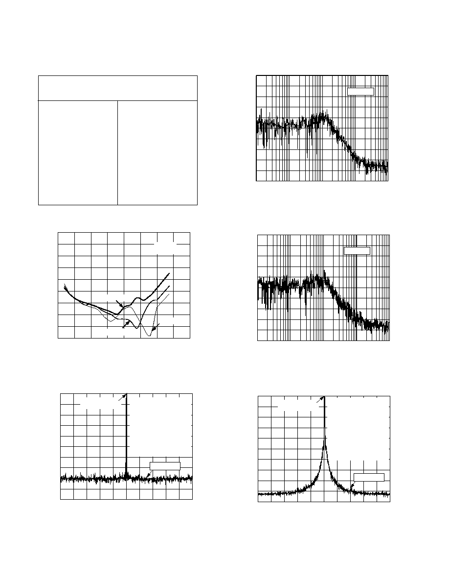
Typical Performance Characteristics
Table I. S-Parameter Data for the ADF4118 RF Input
(Up to 1.8 GHz)
KEYWORD
FREQ-
PARAM-
DATA-
IMPEDANCE-
UNIT
TYPE
FORMAT
OHMS
GHZ
S
MA
R
50
FREQ
MagS11 AngS11
0.95
0.92087
36.961
1.00
0.93788
39.343
1.05
0.9512 40.134
1.10
0.93458
43.747
1.15
0.94782
44.393
1.20
0.96875
46.937
1.25
0.92216
49.6
1.30
0.93755
51.884
1.35
0.96178
51.21
1.40
0.94354
53.55
1.45
0.95189
56.786
1.50
0.97647
58.781
1.55
0.98619
60.545
1.60
0.95459
61.43
1.65
0.97945
61.241
1.70
0.98864
64.051
1.75
0.97399
66.19
1.80
0.97216
63.775
FREQ MagS11
AngS11
0.05
0.89207
2.0571
0.10
0.8886
4.4427
0.15
0.89022
6.3212
0.20
0.96323
2.1393
0.25
0.90566
12.13
0.30
0.90307
13.52
0.35
0.89318
15.746
0.40
0.89806
18.056
0.45
0.89565
19.693
0.50
0.88538
22.246
0.55
0.89699
24.336
0.60
0.89927
25.948
0.65
0.87797
28.457
0.70
0.90765
29.735
0.75
0.88526
31.879
0.80
0.81267
32.681
0.85
0.90357
31.522
0.90
0.92954
34.222
RF INPUT FREQUENCY GHz
0
4.0
0.5
1.5
2.0
2.5
3.0
3.5
35
RF INPUT POWER
dBm
0
15
20
25
30
5
10
1.0
V
DD
= 3V
V
P
= 3V
T
A
= 40 C
T
A
= 85 C
T
A
= 25 C
40
45
Figure 2. Input Sensitivity (ADF4118)
2kHz
1kHz
900MHz
+1kHz
+2kHz
V
DD
= 3V, V
P
= 5V
I
CP
= 1mA
PFD FREQUENCY = 200kHz
LOOP BANDWIDTH = 20kHz
RES. BANDWIDTH = 10Hz
VIDEO BANDWIDTH = 10Hz
SWEEP = 1.9 SECONDS
AVERAGES = 22
REFERENCE
LEVEL = 4.2dBm
OUTPUT POWER
dB
0
50
70
80
90
10
30
60
40
20
100
90.2dBc/Hz
Figure 3. ADF4118 Phase Noise (900 MHz, 200 kHz, 20 kHz)
10dB/DIVISION
R
L
= 40dBc/Hz
RMS NOISE = 0.64
100Hz
FREQUENCY OFFSET FROM 900 MHz CARRIER
1MHz
PHASE NOISE
dBc/Hz
40
80
100
50
70
60
90
110
120
130
140
0.64 rms
Figure 4. ADF4118 Integrated Phase Noise (900 MHz,
200 kHz, 35 kHz, Typical Lock Time: 200
µs)
10dB/DIVISION
R
L
= 40dBc/Hz
RMS NOISE = 0.575
100Hz
FREQUENCY OFFSET FROM 900 MHz CARRIER
1MHz
PHASE NOISE
dBc/Hz
40
70
80
90
100
50
60
110
120
130
140
0.575 rms
Figure 5. ADF4118 Integrated Phase Noise (900 MHz,
200 kHz, 20 kHz, Typical Lock Time: 400
µs)
400kHz
200kHz
900MHz
+200kHz
+400kHz
V
DD
= 3V, V
P
= 5V
I
CP
= 1mA
PFD FREQUENCY = 200kHz
LOOP BANDWIDTH = 20kHz
RES. BANDWIDTH = 1kHz
VIDEO BANDWIDTH = 1kHz
SWEEP = 2.5 SECONDS
AVERAGES = 4
REFERENCE
LEVEL = 3.8dBm
OUTPUT POWER
dB
0
50
70
80
90
10
30
60
40
20
100
91.5dBc
Figure 6. ADF4118 Reference Spurs (900 MHz, 200 kHz,
20 kHz)
ADF4116/ADF4117/ADF4118
7
REV. 0
400kHz
200kHz
900MHz
+200kHz
+400kHz
V
DD
= 3V, V
P
= 5V
I
CP
= 1mA
PFD FREQUENCY = 200kHz
LOOP BANDWIDTH = 35kHz
RES. BANDWIDTH = 1kHz
VIDEO BANDWIDTH = 1kHz
SWEEP = 2.5 SECONDS
AVERAGES = 10
REFERENCE
LEVEL = 4.2dBm
OUTPUT POWER
dB
0
50
70
80
90
10
30
60
40
20
100
90.67dBc
Figure 7. ADF4118 Reference Spurs (900 MHz, 200 kHz,
35 kHz)
400kHz
200kHz
1750MHz
+200kHz
+400kHz
V
DD
= 3V, V
p
= 5V
I
CP
= 1mA
PFD FREQUENCY = 30kHz
LOOP BANDWIDTH = 5kHz
RES. BANDWIDTH = 10kHz
VIDEO BANDWIDTH = 10kHz
SWEEP = 477ms
AVERAGES = 25
REFERENCE
LEVEL = 7.0dBm
OUTPUT POWER
dB
0
50
70
80
90
10
30
60
40
20
100
71.5dBc/Hz
Figure 8. ADF4118 Phase Noise (1750 MHz, 30 kHz,
3 kHz)
10dB/DIVISION
R
L
= 40dBc/Hz
RMS NOISE = 2.0
100Hz
FREQUENCY OFFSET FROM 1.75GHz CARRIER
1MHz
PHASE NOISE
dBc/Hz
40
70
80
90
100
50
60
110
120
130
140
2.0 rms
Figure 9. ADF4118 Integrated Phase Noise (1750 MHz,
30 kHz, 3 kHz)
60kHz
30kHz
1750MHz
+30kHz
+60kHz
REFERENCE
LEVEL = 7.0dBm
OUTPUT POWER
dB
0
50
70
80
90
10
30
60
40
20
100
V
DD
= 3V, V
p
= 5V
I
CP
= 5mA
PFD FREQUENCY = 30kHz
LOOP BANDWIDTH = 5kHz
RES. BANDWIDTH = 300Hz
VIDEO BANDWIDTH = 300Hz
SWEEP = 4.2ms
AVERAGES = 20
72.3dBc
Figure 10. ADF4118 Reference Spurs (1750 MHz,
30 kHz, 3 kHz)
2kHz
1kHz
2800MHz
+1kHz
+2kHz
V
DD
= 3V, V
p
= 5V
I
CP
= 1mA
PFD FREQUENCY = 1MHz
LOOP BANDWIDTH = 100kHz
RES. BANDWIDTH = 10Hz
VIDEO BANDWIDTH = 10Hz
SWEEP = 1.9 SECONDS
AVERAGES = 26
REFERENCE
LEVEL = 10.3dBm
OUTPUT POWER
dB
0
50
70
80
90
10
30
60
40
20
100
85.2dBc/Hz
Figure 11. ADF4118 Phase Noise (2800 MHz, 1 MHz,
100 kHz)
10dB/DIVISION
R
L
= 40dBc/Hz
RMS NOISE = 1.552
100Hz
FREQUENCY OFFSET FROM 2.8 GHz CARRIER
1MHz
PHASE NOISE
dBc/Hz
40
70
80
90
100
50
60
110
120
130
140
1.55 rms
Figure 12. ADF4118 Integrated Phase Noise (2800 MHz,
1 MHz, 100 kHz)
ADF4116/ADF4117/ADF4118
8
REV. 0
2MHz
1MHz
+1MHz
+2MHz
V
DD
= 3V, V
P
= 5V
I
CP
= 1mA
PFD FREQUENCY = 1MHz
LOOP BANDWIDTH = 100kHz
RES. BANDWIDTH = 3kHz
VIDEO BANDWIDTH = 3kHz
SWEEP = 1.4 SECONDS
AVERAGES = 4
REFERENCE
LEVEL = 9.3dBm
OUTPUT POWER
dB
0
50
70
80
90
10
30
60
40
20
100
2800MHz
77.3dBc
Figure 13. ADF4118 Reference Spurs (2800 MHz, 1 MHz,
100 kHz)
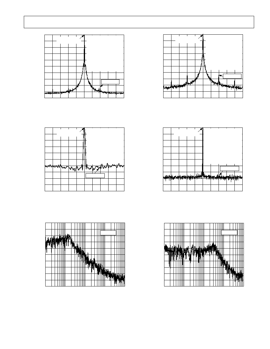
PHASE DETECTOR FREQUENCY kHz
1
10000
100
1000
175
PHASE NOISE
dBc/Hz
145
150
160
170
130
135
10
165
155
140
V
DD
= 3V
V
P
= 5V
Figure 14. ADF4118 Phase Noise (Referred to CP Out-
put) vs. PFD Frequency
40
PHASE NOISE
dBc/Hz
60
80
90
70
100
TEMPERATURE C
20
0
20
40
60
80
100
V
DD
= 3V
V
P
= 5V
Figure 15. ADF4118 Phase Noise vs. Temperature
(900 MHz, 200 kHz, 20 kHz)
40
FIRST REFERENCE SPUR
dBc
60
80
90
70
100
TEMPERATURE C
20
0
20
40
60
80
100
V
DD
= 3V
V
P
= 5V
Figure 16. ADF4118 Reference Spurs vs. Temperature
(900 MHz, 200 kHz, 20 kHz)
0
FIRST REFERENCE SPUR
dBc
5
95
105
TURNING VOLTAGE
1
V
DD
= 3V
V
P
= 5V
2
3
4
5
85
75
65
55
45
35
25
15
5
Figure 17. ADF4118 Reference Spurs (200 kHz) vs.
V
TUNE
(900 MHz, 200 kHz, 20 kHz)
PHASE NOISE
dBc/Hz
60
80
90
70
TEMPERATURE C
0
20
40
60
80
100
V
DD
= 3V
V
P
= 5V
Figure 18. ADF4118 Phase Noise vs. Temperature
(836 MHz, 30 kHz, 3 kHz)
ADF4116/ADF4117/ADF4118
9
REV. 0
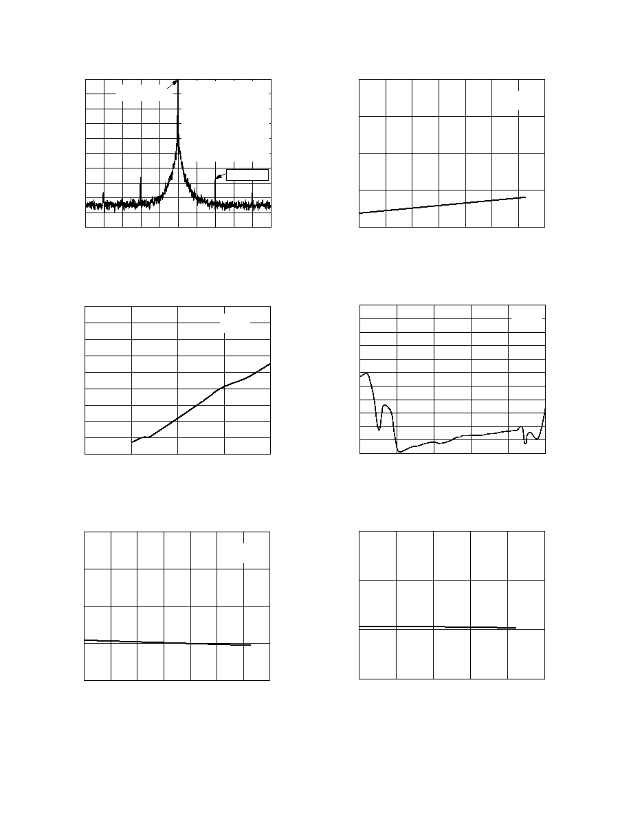
FIRST REFERENCE SPUR
dBc
60
80
90
70
TEMPERATURE C
0
20
40
60
80
100
V
DD
= 3V
V
P
= 5V
100
Figure 19. ADF4118 Reference Spurs vs. Temperature
(836 MHz, 30 kHz, 3 kHz)
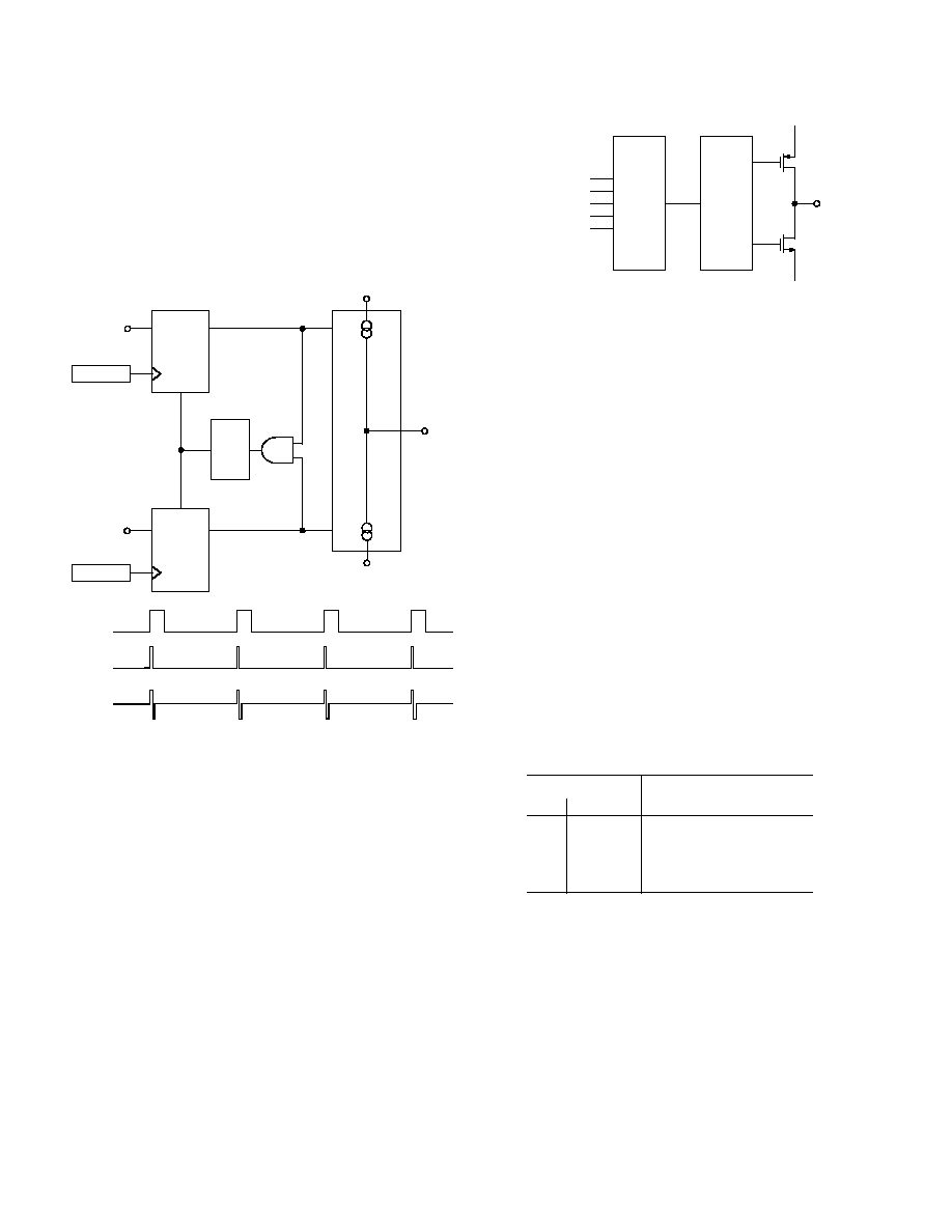
CIRCUIT DESCRIPTION
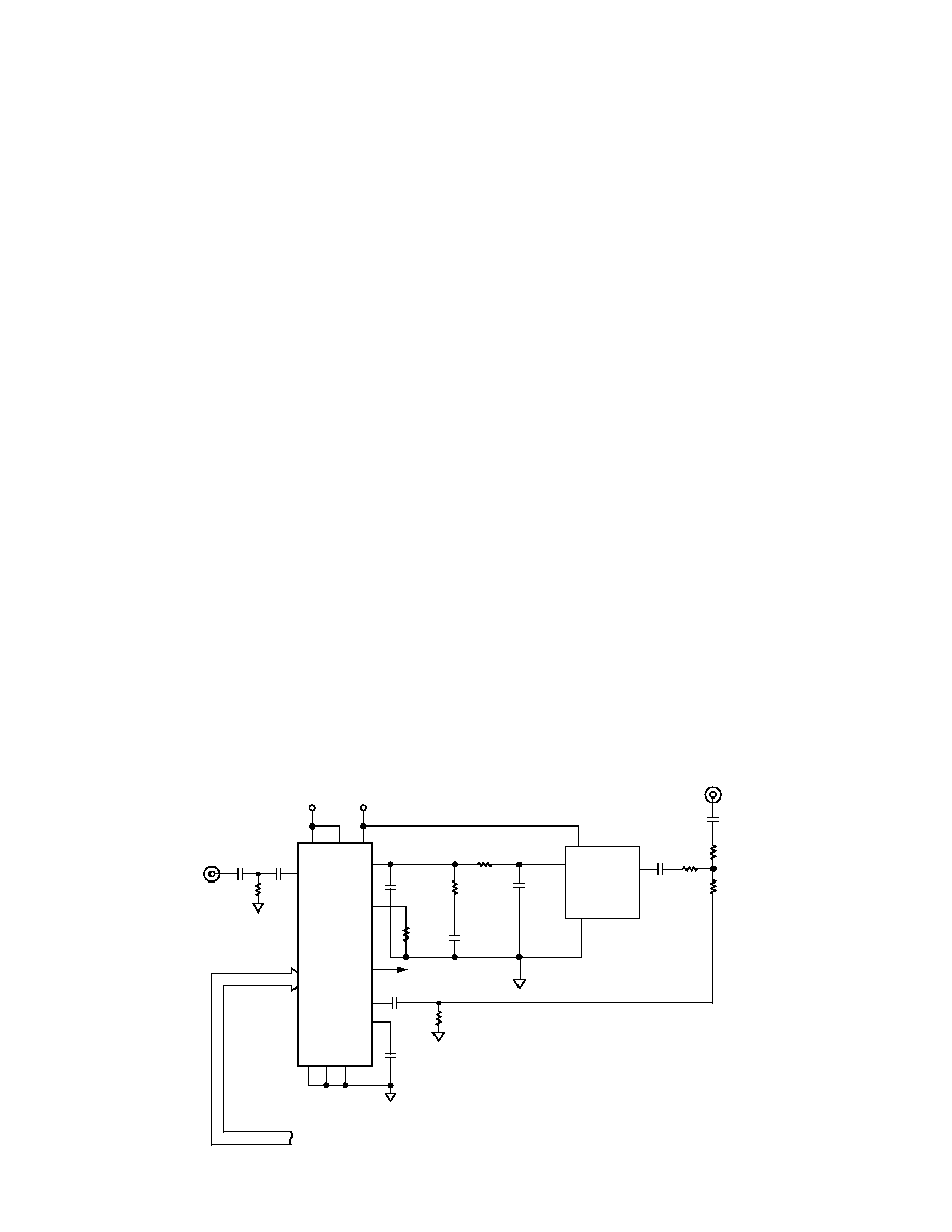
REFERENCE INPUT SECTION
The reference input stage is shown below in Figure 21. SW1
and SW2 are normally-closed switches. SW3 is normally-open.
When power-down is initiated, SW3 is closed and SW1 and SW2
are opened. This ensures that there is no loading of the REF
IN
pin on power-down.
BUFFER
TO R COUNTER
REF
IN
100k
NC
SW2
SW3
NO
NC
SW1
POWER-DOWN
CONTROL
Figure 21. Reference Input Stage
RF INPUT STAGE
The RF input stage is shown in Figure 22. It is followed by a 2-
stage limiting amplifier to generate the CML clock levels needed
for the prescaler.
AV
DD
AGND
500
500
1.6V
BIAS
GENERATOR
RF
IN
A
RF
IN
B
Figure 22. RF Input Stage
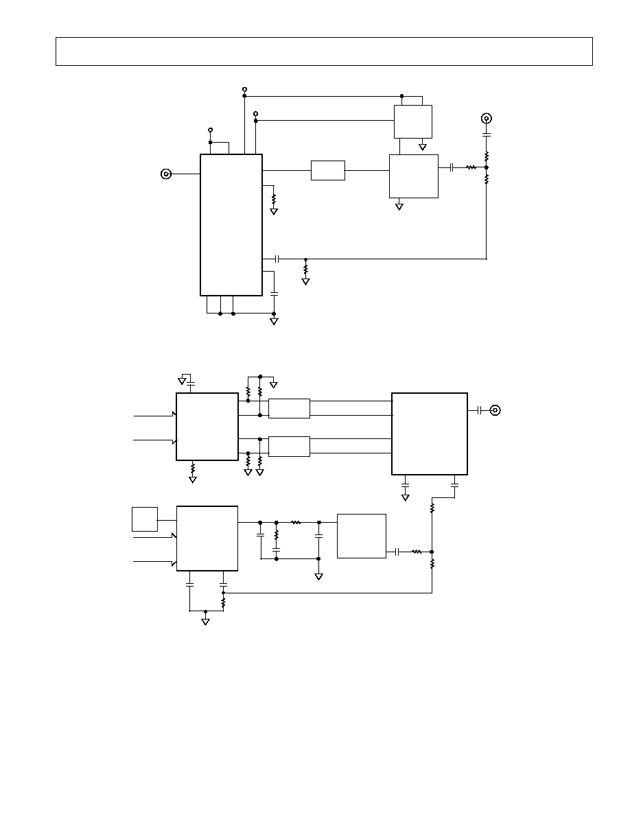
PRESCALER (P/P + 1)
The dual modulus prescale (P/P + 1), along with the A and B
counters, enables the large division ratio, N, to be realized, (N =
PB + A). The dual-modulus prescaler takes the CML clock
from the RF input stage and divides it down to a manageable
frequency for the CMOS A and B counters. The prescaler is
programmable. It can be set in software to 8/9 for the
ADF4116, and set to 32/33 for the ADF4117 and ADF4118.
It is based on a synchronous 4/5 core.
A AND B COUNTERS
The A and B CMOS counters combine with the dual modulus
prescaler to allow a wide ranging division ratio in the PLL
feedback counter. The counters are specified to work when the
prescaler output is 200 MHz or less.
Pulse Swallow Function
The A and B counters, in conjunction with the dual modulus
prescaler make it possible to generate output frequencies which
are spaced only by the Reference Frequency divided by R. The
equation for the VCO frequency is as follows:
f
VCO
= [(P
× B) + A] × f
REFIN
/R
f
VCO
Output Frequency of external voltage controlled oscilla-
tor (VCO).
P
Preset modulus of dual modulus prescaler.
B
Preset Divide Ratio of binary 13-bit counter (3 to 8191).
A
Preset Divide Ratio of binary 5-bit swallow counter
(0 to 31).
f
REFIN
Output frequency of the external reference frequency
oscillator.
R
Preset divide ratio of binary 14-bit programmable refer-
ence counter (1 to 16383).
R COUNTER
The 14-bit R counter allows the input reference frequency to be
divided down to produce the input clock to the phase frequency
detector (PFD). Division ratios from 1 to 16,383 are allowed.
13-BIT B
COUNTER
5-BIT A
COUNTER
PRESCALER
P/P + 1
FROM RF
INPUT STAGE
MODULUS
CONTROL
N = BP + A
LOAD
LOAD
TO PFD
Figure 23. A and B Counters
0
DI
DD
mA
0.0
PRESCALER OUTPUT FREQUENCY MHz
50
100
150
200
0.5
1.0
1.5
2.0
2.5
3.0
Figure 20. DI
DD
vs. Prescaler Output Frequency
(ADF4116, ADF4117, ADF4118)
ADF4116/ADF4117/ADF4118
10
REV. 0
PHASE FREQUENCY DETECTOR (PFD) AND CHARGE
PUMP
The PFD takes inputs from the R counter and N counter and
produces an output proportional to the phase and frequency
difference between them. Figure 24 is a simplified schematic.
The PFD includes a fixed delay element which sets the width of
the antibacklash pulse. This is typically 3 ns. This pulse ensures
that there is no dead zone in the PFD transfer function and
gives a consistent reference spur level.
DELAY
U3
CLR1
Q1
D1
CP
DOWN
UP
HI
U1
CLR2
Q2
D2
U2
HI
N DIVIDER
R DIVIDER
V
P
CHARGE
PUMP
CP GND
R DIVIDER
CP OUTPUT
N DIVIDER
Figure 24. PFD Simplified Schematic and Timing (In Lock)
MUXOUT AND LOCK DETECT
The output multiplexer on the ADF4116 family allows the
user to access various internal points on the chip. The state of
MUXOUT is controlled by M3, M2 and M1 in the function
latch. Table VI shows the full truth table. Figure 25 shows the
MUXOUT section in block diagram form.
CONTROL
MUX
DV
DD
MUXOUT
DGND
ANALOG LOCK DETECT
DIGITAL LOCK DETECT
R COUNTER OUTPUT
N COUNTER OUTPUT
SDOUT
Figure 25. MUXOUT Circuit
Lock Detect
MUXOUT can be programmed for two types of lock detect:
Digital Lock Detect and Analog Lock Detect.
Digital Lock Detect is active high. It is set high when the phase
error on three consecutive phase detector cycles is less than 15 ns.
It will stay set high until a phase error of greater than 25 ns is
detected on any subsequent PD cycle.
The N-channel open-drain analog lock detect should be oper-
ated with an external pull-up resistor of 10 k
nominal. When
lock has been detected it is high with narrow low-going pulses.
INPUT SHIFT REGISTER
The ADF4116 family digital section includes a 21-bit input shift
register, a 14-bit R counter and a`-bit N counter, comprising
a 5-bit A counter and a 13-bit B counter. Data is clocked into
the 21-bit shift register on each rising edge of CLK. The data is
clocked in MSB first. Data is transferred from the shift register
to one of four latches on the rising edge of LE. The destination
latch is determined by the state of the two control bits (C2, C1)
in the shift register. These are the two LSBs DB1, DB0 as
shown in the timing diagram of Figure 1. The truth table for
these bits is shown in Table VII. Table II shows a summary
of how the latches are programmed.
Table II. C2, C1 Truth Table
Control Bits
C2
C1
Data Latch
0
0
R Counter
0
1
N Counter (A and B)
1
0
Function Latch
1
1
Initialization Latch
ADF4116/ADF4117/ADF4118
11
REV. 0
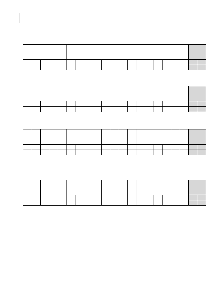
Table III. ADF4116 Family Latch Summary
LOCK
DETECT
PRECISION
TEST
MODE BITS
DB20
DB19
DB18
DB17
DB16
DB15
DB14
DB13
DB12
DB11
DB9
DB8
DB7
DB6
DB5
DB4
DB3
DB2
DB1
DB0
DB10
LDP
T4
T3
T2
T1
R14
R13
R12
R11
R10
R8
R7
R6
R5
R4
R3
R2
R1
C2 (0)
C1 (0)
R9
14-BIT REFERENCE COUNTER, R
CONTROL
BITS
DB20
DB19
DB18
DB17
DB16
DB15
DB14
DB13
DB12
DB11
DB9
DB8
DB7
DB6
DB5
DB4
DB3
DB2
DB1
DB0
DB10
G1
B13
B12
B11
B10
B9
B8
B7
B6
B5
B3
B2
B1
A5
A4
A3
A2
A1
C2 (0)
C1 (1)
B4
CONTROL
BITS
13-BIT B COUNTER
5-BIT A COUNTER
CP GAIN
DB19
DB18
DB17
DB16
DB15
DB14
DB13
DB12
DB11
DB9
DB8
DB7
DB6
DB5
DB4
DB3
DB2
DB1
DB0
DB10
TC4
TC3
TC2
TC1
F6
F4
F3
F2
M3
M2
M1
PD1
F1
C2 (1)
C1 (0)
CONTROL
BITS
MUXOUT
CONTROL
POWER-
DOWN 2
POWER-
DOWN 1
COUNT
RESETER
PD
POLARITY
FASTLOCK
ENABLE
CP
THREE-
STATE
FASTLOCK
MODE
TIMER COUNTER
CONTROL
DB20
DB19
DB18
DB17
DB16
DB15
DB14
DB13
DB12
DB11
DB9
DB8
DB7
DB6
DB5
DB4
DB3
DB2
DB1
DB0
DB10
PD2
TC4
TC3
TC2
TC1
F6
F4
F3
F2
M3
M2
M1
PD1
F1
C2 (1)
C1 (1)
CONTROL
BITS
MUXOUT
CONTROL
POWER-
DOWN 2
POWER-
DOWN 1
COUNT
RESETER
PD
POLARITY
FASTLOCK
ENABLE
CP
THREE-
STATE
FASTLOCK
MODE
TIMER COUNTER
CONTROL
REFERENCE COUNTER LATCH
AB COUNTER LATCH
FUNCTION LATCH
INITIALIZATION LATCH
RESERVED
RESERVED
PD2
X
DB20
X
RESERVED
X
X
X
RESERVED
RESERVED
X
X
RESERVED
X
X
X
ADF4116/ADF4117/ADF4118
12
REV. 0
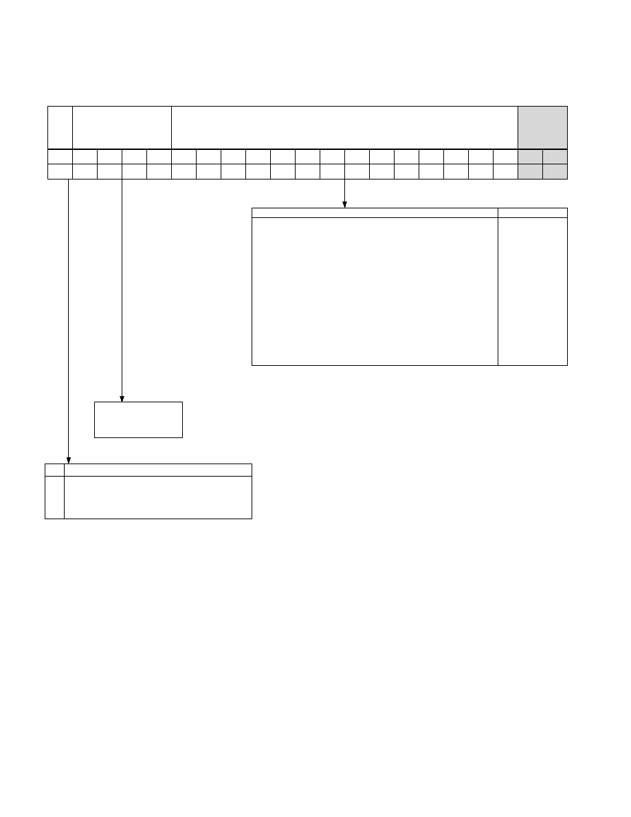
Table IV. Reference Counter Latch Map
R14
0
0
0
0
·
·
·
1
1
1
1
R13
0
0
0
0
·
·
·
1
1
1
1
R12
0
0
0
0
·
·
·
1
1
1
1
R3
R2
R1
DIVIDE RATIO
··········
··········
··········
··········
··········
··········
··········
··········
··········
··········
··········
··········
0
0
0
1
·
·
·
1
1
1
1
0
1
1
0
·
·
·
0
0
1
1
1
0
1
0
·
·
·
0
1
0
1
1
2
3
4
·
·
·
163 80
163 81
163 82
163 83
TEST MODE BITS SHOULD
BE SET TO 0000 FOR
NORMAL OPERATION
OPERATION
LDP
3 CONSECUTIVE CYCLES OF PHASE DELAY LESS THAN
15ns MUST OCCUR BEFORE LOCK DETECT IS SET.
5 CONSECUTIVE CYCLES OF PHASE DELAY LESS THAN
15ns MUST OCCUR BEFORE LOCK DETECT IS SET.
0
1
LOCK
DETECT
PRECISION
TEST
MODE BITS
DB20
DB19
DB18
DB17
DB16
DB15
DB14
DB13
DB12
DB11
DB9
DB8
DB7
DB6
DB5
DB4
DB3
DB2
DB1
DB0
DB10
LDP
T4
T3
T2
T1
R14
R13
R12
R11
R10
R8
R7
R6
R5
R4
R3
R2
R1
C2 (0)
C1 (0)
R9
14-BIT REFERENCE COUNTER, R
CONTROL
BITS
ADF4116/ADF4117/ADF4118
13
REV. 0
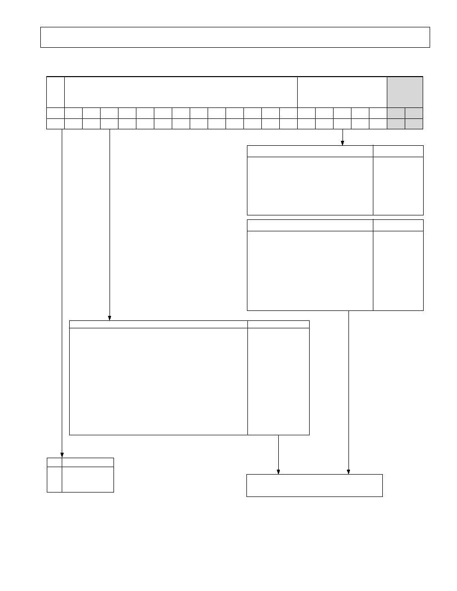
Table V. AB Counter Latch Map
CURRENT SETTINGS
LDP
250 A
0
1
A5
X
X
·
·
X
X
A4
X
X
·
·
X
X
A3
0
0
·
·
1
1
A2
0
0
·
·
1
1
A1
0
1
·
·
0
1
A COUNTER
DIVIDE RATIO
0
1
·
·
6
7
B13
0
0
0
0
·
·
·
1
1
1
1
B12
0
0
0
0
·
·
·
1
1
1
1
B11
0
0
0
0
·
·
·
1
1
1
1
B3
B2
B1
B COUNTER DIVIDE RATIO
··········
··········
··········
··········
··········
··········
··········
··········
··········
··········
··········
··········
0
0
0
1
·
·
·
1
1
1
1
0
1
1
0
·
·
·
0
0
1
1
1
0
1
0
·
·
·
0
1
0
1
NOT ALLOWED
NOT ALLOWED
3
4
·
·
·
8188
8189
8190
8191
ADF4116
A5
0
0
0
·
·
1
1
1
A4
0
0
0
·
·
1
1
1
A3
0
0
0
·
·
1
1
1
A2
0
0
1
·
·
0
1
1
A1
0
1
0
·
·
1
0
1
A COUNTER
DIVIDE RATIO
0
1
2
·
·
29
30
31
ADF4117/ADF4118
1mA
N = BP + A, P IS PRESCALER VALUE. B MUST BE GREATER
THAN OR EQUAL TO A. FOR CONTINUOUSLY ADJACENT
VALUES OF N
X
F
REF
, N
MIN
IS (P
2
-P).
DB20
DB19
DB18
DB17
DB16
DB15
DB14
DB13
DB12
DB11
DB9
DB8
DB7
DB6
DB5
DB4
DB3
DB2
DB1
DB0
DB10
G1
B13
B12
B11
B10
B9
B8
B7
B6
B5
B3
B2
B1
A5
A4
A3
A2
A1
C2 (0)
C1 (1)
B4
CONTROL
BITS
13-BIT B COUNTER
5-BIT A COUNTER
CP GAIN
ADF4116/ADF4117/ADF4118
14
REV. 0
Table VI. Function Latch Map
M3
0
0
0
0
1
1
1
1
M2
0
0
1
1
0
0
1
1
M1
0
1
0
1
0
1
0
1
OUTPUT
THREE-STATE OUTPUT
DIGITAL LOCK DETECT
(ACTIVE HIGH)
N DIVIDER OUTPUT
AV
DD
R DIVIDER OUTPUT
ANALOG LOCK DETECT
(N CHANNEL OPEN DRAIN)
SERIAL DATA OUTPUT
(INVERSE POLARITY OF
SERIAL DATA INPUT)
DGND
TC4
0
0
0
0
0
0
0
0
1
1
1
1
1
1
1
1
TC3
0
0
0
0
1
1
1
1
0
0
0
0
1
1
1
1
TC2
0
0
1
1
0
0
1
1
0
0
1
1
0
0
1
1
TC1
0
1
0
1
0
1
0
1
0
1
0
1
0
1
0
1
TIMEOUT
(PFD CYCLES)
3
7
11
15
19
23
27
31
35
39
43
47
51
55
59
63
F1
0
1
COUNTER
OPERATION
NORMAL
R, A, B COUNTERS
HELD IN RESET
F2
0
1
PD POLARITY
NEGATIVE
POSITIVE
F3
0
1
CHARGE PUMP
OUTPUT
NORMAL
3-STATE
0
1
1
1
CE PIN PD2 PD1
MODE
X
X
0
1
X
0
1
1
F6
X
0
1
FASTLOCK MODE
FASTLOCK DISABLED
FASTLOCK MODE 1
FASTLOCK MODE 2
F4
0
1
1
ASYNCHRONOUS POWER-DOWN
NORMAL OPERATION
ASYNCHRONOUS POWER-DOWN
SYNCHRONOUS POWER-DOWN
DB19
DB18
DB17
DB16
DB15
DB14
DB13
DB12
DB11
DB9
DB8
DB7
DB6
DB5
DB4
DB3
DB2
DB1
DB0
DB10
TC4
TC3
TC2
TC1
F6
F4
F3
F2
M3
M2
M1
PD1
F1
C2 (1)
C1 (0)
CONTROL
BITS
MUXOUT
CONTROL
POWER-
DOWN 2
POWER-
DOWN 1
COUNT
RESETER
PD
POLARITY
FASTLOCK
ENABLE
CP
THREE-
STATE
FASTLOCK
MODE
TIMER COUNTER
CONTROL
RESERVED
RESERVED
PD2
X
DB20
X
RESERVED
X
X
X
ADF4116/ADF4117/ADF4118
15
REV. 0
Table VII. Initialization Latch Map
M3
0
0
0
0
1
1
1
1
M2
0
0
1
1
0
0
1
1
M1
0
1
0
1
0
1
0
1
OUTPUT
THREE-STATE OUTPUT
DIGITAL LOCK DETECT
(ACTIVE HIGH)
N DIVIDER OUTPUT
AV
DD
R DIVIDER OUTPUT
ANALOG LOCK DETECT
(N CHANNEL OPEN DRAIN)
SERIAL DATA OUTPUT
(INVERSE POLARITY OF
SERIAL DATA INPUT)
DGND
TC4
0
0
0
0
0
0
0
0
1
1
1
1
1
1
1
1
TC3
0
0
0
0
1
1
1
1
0
0
0
0
1
1
1
1
TC2
0
0
1
1
0
0
1
1
0
0
1
1
0
0
1
1
TC1
0
1
0
1
0
1
0
1
0
1
0
1
0
1
0
1
TIMEOUT
(PFD CYCLES)
3
7
11
15
19
23
27
31
35
39
43
47
51
55
59
63
F1
0
1
COUNTER
OPERATION
NORMAL
R, A, B COUNTERS
HELD IN RESET
F2
0
1
PD POLARITY
NEGATIVE
POSITIVE
F3
0
1
CHARGE PUMP
OUTPUT
NORMAL
THREE-STATE
0
1
1
1
CE PIN PD2 PD1
MODE
ASYNCHRONOUS POWER-DOWN
NORMAL OPERATION
ASYNCHRONOUS POWER-DOWN
SYNCHRONOUS POWER-DOWN
X
X
0
1
X
0
1
1
F6
X
0
1
FASTLOCK MODE
FASTLOCK DISABLED
FASTLOCK MODE 1
FASTLOCK MODE 2
F4
0
1
1
DB20
DB19
DB18
DB17
DB16
DB15
DB14
DB13
DB12
DB11
DB9
DB8
DB7
DB6
DB5
DB4
DB3
DB2
DB1
DB0
DB10
PD2
TC4
TC3
TC2
TC1
F6
F4
F3
F2
M3
M2
M1
PD1
F1
C2 (1)
C1 (1)
CONTROL
BITS
MUXOUT
CONTROL
POWER-
DOWN 2
POWER-
DOWN 1
COUNT
RESETER
PD
POLARITY
FASTLOCK
ENABLE
CP
THREE-
STATE
FASTLOCK
MODE
TIMER COUNTER
CONTROL
RESERVED
RESERVED
X
X
RESERVED
X
X
X

ADF4116/ADF4117/ADF4118
16
REV. 0
THE FUNCTION LATCH
With C2, C1 set to 1, 0, the on-chip function latch will be pro-
grammed. Table VI shows the input data format for programming
the Function Latch.
Counter Reset
DB2 (F1) is the counter reset bit. When this is "1," the R counter
and the A, B counters are reset. For normal operation this bit
should be "0." Upon powering up, the F1 bit needs to be disabled,
the N counter resumes counting in "close" alignment with the R counter.
(The maximum error is one prescaler cycle.)
Power-Down
DB3 (PD1) and DB19 (PD2) on the ADF4116 family, provide
programmable power-down modes. They are enabled by the
CE pin.
When the CE pin is low, the device is immediately disabled
regardless of the states of PD2, PD1.
In the programmed asynchronous power-down, the device pow-
ers down immediately after latching a "1" into bit PD1, with the
condition that PD2 has been loaded with a "0."
In the programmed synchronous power-down, the device power
down is gated by the charge pump to prevent unwanted fre-
quency jumps. Once the power-down is enabled by writing a
"1" into bit PD1 (on condition that a "1" has also been loaded
to PD2), then the device will go into power-down after the first
successive charge pump event.
When a power down is activated (either synchronous or asynchro-
nous mode including CE-pin-activated power down), the
following events occur:
All active dc current paths are removed.
The R, N and timeout counters are forced to their load state
conditions.
The charge pump is forced into three-state mode.
The digital clock detect circuitry is reset.
The RF
IN
input is debiased.
The oscillator input buffer circuitry is disabled.
The input register remains active and capable of loading and
latching data.
MUXOUT Control
The on-chip multiplexer is controlled by M3, M2, M1 on the
ADF4116 family. Table VI shows the truth table.
Phase Detector Polarity
DB7 (F2) of the function latch sets the Phase Detector Polarity.
When the VCO characteristics are positive this should be set to
"1." When they are negative it should be set to "0."
Charge Pump Three-State
This bit puts the charge pump into three-state mode when pro-
grammed to a "1." It should be set to "0" for normal operation.
Fastlock Enable Bit
DB9 of the Function Latch is the Fastlock Enable Bit. Only
when this is "1" is Fastlock enabled.
Fastlock Mode Bit
DB11 of the Function Latch is the Fastlock Mode bit. When
Fastlock is enabled, this bit determines which Fastlock Mode is
used. If the Fastlock Mode bit is "0" then Fastlock Mode 1 is
selected and if the Fastlock Mode bit is "1," then Fastlock
Mode 2 is selected.
If Fastlock is not enabled (DB9 = "0"), then DB11 (ADF4116)
determines the state of the FL
O
output. FL
O
state will be the
same as that programmed to DB11.
Fastlock Mode 1
In the ADF4116 family, the output level of FL
O
is programmed
to a low state and the charge pump current is switched to the
high value (1 mA). FL
O
is used to switch a resistor in the loop
filter and ensure stability while in Fastlock by altering the loop
bandwidth.
The device enters Fastlock by having a "1" written to the CP
Gain bit in the N register. The device exits Fastlock by having a
"0" written to the CP Gain bit in the N register.
Fastlock Mode 2
In the ADF4116 family, the output level of FL
O
is programmed
to a low state and the charge pump current is switched to the high
value (1 mA). FL
O
is used to switch a resistor in the loop filter and
ensure stability while in Fastlock by altering the loop bandwidth.
The device enters Fastlock by having a "1" written to the CP
Gain bit in the N register. The device exits Fastlock under the
control of the Timer Counter. After the timeout period deter-
mined by the value in TC4TC1, the CP Gain bit in the N
register is automatically reset to "0" and the device reverts to
normal mode instead of Fastlock.
Timer Counter Control
In the ADF4116 family, the user has the option of switching
between two charge pump current values to speed up locking to
a new frequency.
When using the Fastlock feature with the ADF4116 family, the
normal sequence of events is as follows:
The user must make sure that Fastlock is enabled. Set DB9 of the
ADF4116 family to "1." The user must also choose which Fastlock
Mode to use. As discussed in the previous section, Fastlock
Mode 2 uses the values in the Timer Counter to determine the
timeout period before reverting to normal mode operation after
Fastlock. Fastlock Mode 2 is chosen by setting DB11 of the
ADF4116 family to "1."
The user must also decide how long they want the high current
(1 mA) to stay active before reverting to low current (250
µA).
This is controlled by the Timer Counter Control Bits DB14 to
DB11 (TC4TC1) in the Function Latch. The truth table is
given in Table VI.
Now, when the user wishes to program a new output frequency,
they can simply program the A, B counter latch with new values
for A and B. At the same time they can set the CP Gain bit to a
"1," which sets the charge pump 1 mA for a period of time deter-
mined by TC4TC1. When this time is up, the charge pump
current reverts to 250
µA. At the same time the CP Gain Bit in
the A, B Counter latch is reset to 0 and is now ready for the
next time that the user wishes to change the frequency again.

ADF4116/ADF4117/ADF4118
17
REV. 0
The Initialization Latch
When C2, C1 = 1, 1 then the Initialization Latch is programmed.
This is essentially the same as the Function Latch (programmed
when C2, C1 = 1, 0).
However, when the Initialization Latch is programmed there is a
additional internal reset pulse applied to the R and N counters.
This pulse ensures that the N counter is at load point when the
N counter data is latched and the device will begin counting in
close phase alignment.
If the Latch is programmed for synchronous power-down (CE
pin is High; PD1 bit is High; PD2 bit is Low), the internal pulse
also triggers this power-down. The prescaler reference and the
oscillator input buffer are unaffected by the internal reset pulse and
so close phase alignment is maintained when counting resumes.
When the first N counter data is latched after initialization, the
internal reset pulse is again activated. However, successive N
counter loads after this will not trigger the internal reset pulse.
Device Programming After Initial Power-Up
After initially powering up the device, there are three ways to
program the device.
Initialization Latch Method
Apply V
DD
.
Program the Initialization Latch ("11" in 2 LSBs of input word).
Make sure that F1 bit is programmed to "0." Then do an R load
("00" in 2 LSBs). Then do an N load ("01" in 2 LSBs). When the
Initialization Latch is loaded, the following occurs:
1. The function latch contents are loaded.
2. An internal pulse resets the R, N and timeout counters to
load state conditions and also three-states the charge pump.
Note that the prescaler bandgap reference and the oscillator
input buffer are unaffected by the internal reset pulse,
allowing close phase alignment when counting resumes.
3. Latching the first N counter data after the initialization word
will activate the same internal reset pulse. Successive N loads
will not trigger the internal reset pulse unless there is another
initialization.
The CE Pin Method
Apply V
DD
.
Bring CE low to put the device into power-down. This is an
asynchronous power-down in that it happens immediately.
Program the Function Latch (10). Program the R Counter
Latch (00). Program the N Counter Latch (01). Bring CE high
to take the device out of power-down. The R and N counter will
now resume counting in close alignment.
Note that after CE goes high, a duration of 1
µs may be required
for the prescaler bandgap voltage and oscillator input buffer bias
to reach steady state.
CE can be used to power the device up and down in order to
check for channel activity. The input register does not need to
be reprogrammed each time the device is disabled and enabled
as long as it has been programmed at least once after V
CC
was
initially applied.
The Counter Reset Method
Apply V
DD
.
Do a Function Latch Load ("10" in 2 LSBs). As part of this,
load "1" to the F1 bit. This enables the counter reset. Do an R
Counter Load ("00" in 2 LSBs). Do an N Counter Load ("01"
in 2 LSBs). Do a Function Latch Load ("10" in 2 LSBs). As
part of this, load "0" to the F1 bit. This disables the counter reset.
This sequence provides the same close alignment as the initial-
ization method. It offers direct control over the internal reset.
Note that counter reset holds the counters at load point and
three-states the charge pump, but does not trigger synchronous
power-down. The counter reset method requires an extra func-
tion latch load compared to the initialization latch method.
ADF4116/ADF4117/ADF4118
18
REV. 0
APPLICATIONS SECTION
Local Oscillator for GSM Base Station Transmitter
Figure 26 shows the ADF4117/ADF4118 being used with a
VCO to produce the LO for a GSM base station transmitter.
The reference input signal is applied to the circuit at FREF
IN
and, in this case, is terminated in 50
. Typical GSM system
would have a 13 MHz TCXO driving the Reference Input
without any 50
termination. In order to have a channel
spacing of 200 kHz (the GSM standard), the reference input
must be divided by 65, using the on-chip reference divider of
the ADF4117/ADF1118.
The charge pump output of the ADF4117/ADF1118 (Pin 2)
drives the loop filter. In calculating the loop filter component
values, a number of items need to be considered. In this example,
the loop filter was designed so that the overall phase margin for
the system would be 45 degrees. Other PLL system specifica-
tions are given below:
K
D
= 1 mA
K
V
= 12 MHz/V
Loop Bandwidth = 20 kHz
F
REF
= 200 kHz
N = 4500
Extra Reference Spur Attenuation = 10 dB
All of these specifications are needed and used to come up with
the loop filter components values shown in Figure 27.
The loop filter output drives the VCO, which, in turn, is fed
back to the RF input of the PLL synthesizer and also drives
the RF Output terminal. A T-circuit configuration provides
50
matching between the VCO output, the RF output and
the RF
IN
terminal of the synthesizer.
In a PLL system, it is important to know when the system is in
lock. In Figure 26, this is accomplished by using the MUXOUT
signal from the synthesizer. The MUXOUT pin can be pro-
grammed to monitor various internal signals in the synthesizer.
One of these is the LD or lock-detect signal.
VCO190-902T
V
CC
18
100pF
100pF
18
18
RF
OUT
V
DD
V
P
AV
DD
DV
DD
ADF4117/
ADF4118
V
P
0.15nF
620pF
3.3k
7
15
16
2
14
6
5
8
FREF
IN
1000pF 1000pF
51
MUXOUT
LOCK
DETECT
51
100pF
3
4
9
100pF
CPGND
AGND
DGND
RF
IN
A
RF
IN
B
CE
CLK
DATA
LE
SPI-COMPATIBLE SERIAL BUS
DECOUPLING CAPACITORS (10 F/10pF) ON AV
DD
, DV
DD
, V
P
OF THE
ADF4117/ADF4118 AND ON V
CC
OF THE VCO190-902T HAVE BEEN
OMITTED FROM THE DIAGRAM TO AID CLARITY.
FL
O
CP
10k
1.5nF
27k
REF
IN
Figure 26. Local Oscillator for GSM Base Station
SHUTDOWN CIRCUIT
The attached circuit in Figure 27 shows how to shut down both
the ADF4116 family and the accompanying VCO. The ADG702
switch goes open circuit when a Logic 1 is applied to the IN
input. The low-cost switch is available in both SOT-23 and
micro SOIC packages.
DIRECT CONVERSION MODULATOR
In some applications a direct conversion architecture can be used
in base station transmitters. Figure 28 shows the combination
available from ADI to implement this solution.
The circuit diagram shows the AD9761 being used with the
AD8346. The use of dual integrated DACs such as the AD9761
with specified
±0.02 dB and ±0.004 dB gain and offset match-
ing characteristics ensures minimum error contribution (over
temperature) from this portion of the signal chain.
The Local Oscillator (LO) is implemented using the ADF4117/
ADF4118. In this case, the OSC 3B1-13M0 provides the
stable 13 MHz reference frequency. The system is designed
for a 200 kHz channel spacing and an output center frequency
of 1960 MHz. The target application is a WCDMA base sta-
tion transmitter. Typical phase noise performance from this LO
is 85 dBc/Hz at a 1 kHz offset. The LO port of the AD8346 is
driven in single-ended fashion. LOIN is ac-coupled to ground
with the 100 pF capacitor and LOIP is driven through the ac-
coupling capacitor from a 50
source. An LO drive level of
between 6 dBm and 12 dBm is required. The circuit of Figure
28 gives a typical level of 8 dBm.
The RF output is designed to drive a 50
load but must be
ac-coupled as shown in Figure 28. If the I and Q inputs are driven
in quadrature by 2 V p-p signals, the resulting output power will
be around 10 dBm.
ADF4116/ADF4117/ADF4118
19
REV. 0
INTERFACING
The ADF4116 family has a simple SPI-compatible serial inter-
face for writing to the device. SCLK, SDATA and LE control
the data transfer. When LE (Latch Enable) goes high, the 24 bits
which have been clocked into the input register on each rising
edge of SCLK will get transferred to the appropriate latch. See
Figure 1 for the Timing Diagram and Table II for the Latch
Truth Table.
V
DD
V
P
AV
DD
DV
DD
ADF4116/
ADF4117/
ADF4118
V
P
10k
VCO
V
CC
GND
18
100pF
100pF
18
18
RF
OUT
7
15
16
2
1
6
5
8
FREF
IN
51
100pF
3
4
9
100pF
CPGND
AGND
DGND
RF
IN
A
RF
IN
B
DECOUPLING CAPACITORS AND INTERFACE SIGNALS HAVE
BEEN OMITTED FROM THE DIAGRAM TO AID CLARITY.
FL
O
CP
CE
POWER-DOWN CONTROL
V
DD
S
IN
D
GND
LOOP
FILTER
ADG702
REF
IN
Figure 27. Local Oscillator Shutdown Circuit
LOW-PASS
FILTER
R
SET
ADF4118
VCO190-1960T
18
100pF
18
REF
IN
100pF
RF
IN
A
RF
IN
B
CP
SERIAL
DIGITAL
NTERFACE
TCXO
OSC 3B1-13M0
100pF
51
18pF
1k
10k
6.8nF
18
RF
OUT
POWER SUPPLY CONNECTIONS AND DECOUPLING CAPACITORS
ARE OMITTED FROM DIAGRAM FOR CLARITY.
AD9761
T
X
DAC
REFIO
FS ADJ
MODULATED
DIGITAL
DATA
QOUTB
IOUTA
IOUTB
QOUTA
LOW-PASS
FILTER
IBBP
QBBP
IBBP
QBBP
AD8346
LOIN
LOIP
VOUT
100pF
100pF
2k
0.1 F
100pF
680pF
Figure 28. Direct Conversion Transmitter Solution
The maximum allowable serial clock rate is 20 MHz. This means
that the maximum update rate possible for the device is 833 kHz or
one update every 1.2 microseconds. This is certainly more than
adequate for systems which will have typical lock times in hun-
dreds of microseconds.
ADF4116/ADF4117/ADF4118
20
REV. 0
ADuC812 Interface
Figure 29 shows the interface between the ADF4116 family and
the ADuC812 microconverter. Since the ADuC812 is based on
an 8051 core, this interface can be used with any 8051-based
microcontroller. The microconverter is set up for SPI Master
Mode with CPHA = 0. To initiate the operation, the I/O port
driving LE is brought low. Each latch of the ADF4116 family
needs a 24-bit word. This is accomplished by writing three 8-bit
bytes from the microconverter to the device. When the third
byte has been written the LE input should be brought high to
complete the transfer.
SCLOCK
MOSI
I/O PORTS
ADuC812
SCLK
SDATA
LE
CE
MUXOUT
(LOCK DETECT)
ADF4116/
ADF4117/
ADF4118
Figure 29. ADuC812 to ADF4116 Family Interface
On first applying power to the ADF4116 family, it needs three
writes (one each to the R counter latch, the N counter latch and
the initialization latch) for the output to become active.
I/O port lines on the ADuC812 are also used to control power-
down (CE input) and to detect lock (MUXOUT configured as
lock detect and polled by the port input).
When operating in the mode described, the maximum SCLOCK
rate of the ADuC812 is 4 MHz. This means that the maximum
rate at which the output frequency can be changed will be 166 kHz.
ADSP-2181 Interface
Figure 30 shows the interface between the ADF4116 family and
the ADSP-21xx Digital Signal Processor. The ADF4116 family
needs a 21-bit serial word for each latch write. The easiest way
to accomplish this using the ADSP-21xx family is to use the
Autobuffered Transmit Mode of operation with Alternate Fram-
ing. This provides a means for transmitting an entire block of
serial data before an interrupt is generated.
SCLK
DT
I/O FLAGS
ADSP-21xx
SCLK
SDATA
LE
CE
MUXOUT
(LOCK DETECT)
ADF4116/
ADF4117/
ADF4118
TFS
Figure 30. ADSP-21xx to ADF4116 Family Interface
Set up the word length for 8 bits and use three memory loca-
tions for each 24-bit word. To program each 21-bit latch, store
the three 8-bit bytes, enable the Autobuffered mode and then
write to the transmit register of the DSP. This last operation
initiates the autobuffer transfer.
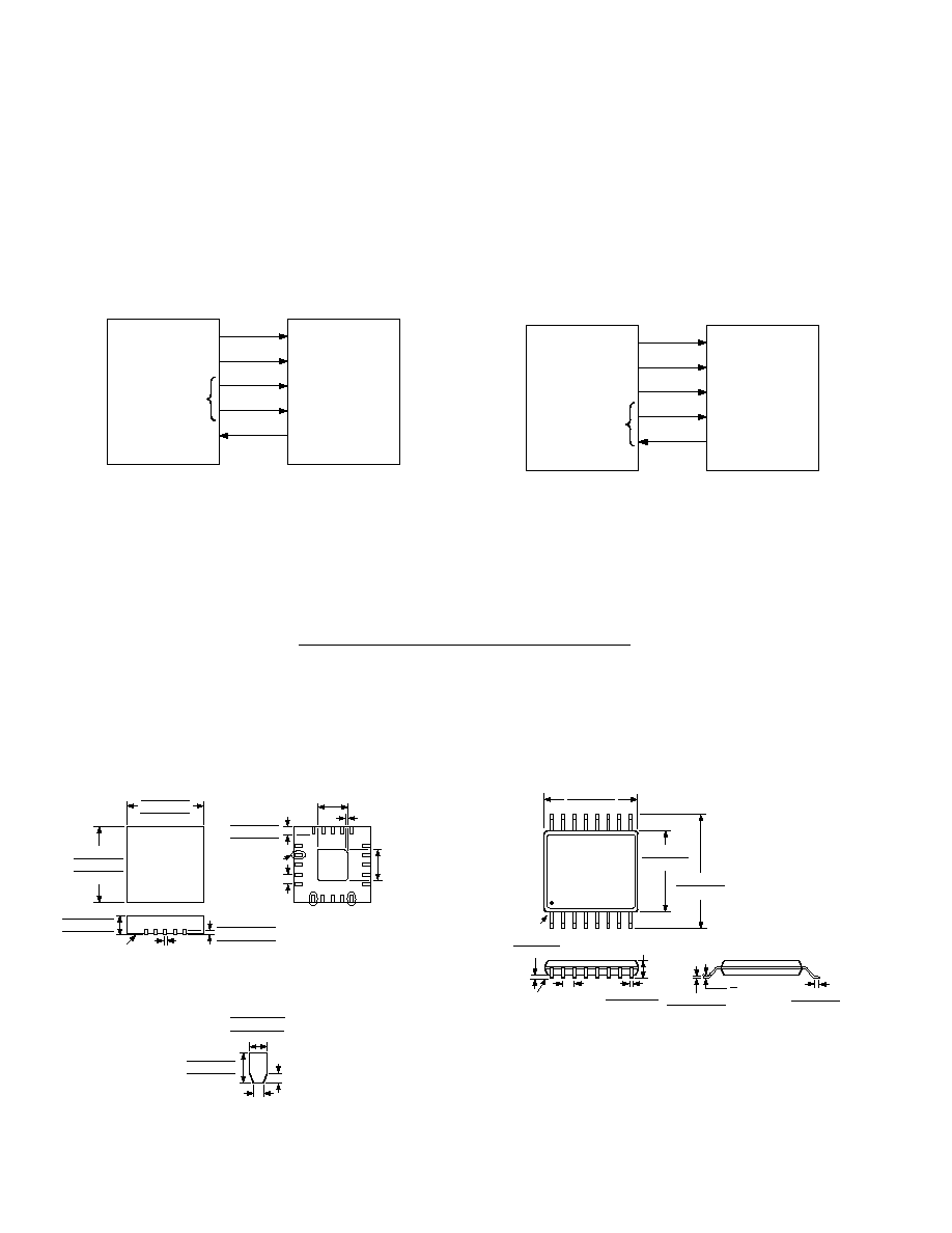
OUTLINE DIMENSIONS
Dimensions shown in inches and (mm).
Chip Scale
(CP-20)
1
20
5
6
10
16
11
15
BOTTOM VIEW
(ROTATED 180 )
0.014 (0.35) 45°
0.018 (0.45)
0.016 (0.40)
0.014 (0.35)
0.079 (2.0) REF
0.079
(2.0)
REF
DETAIL E
0.020 (0.5) REF
LEAD PITCH
0.0079 (0.20)
REF
0.0083 (0.211)
0.0079 (0.200)
0.0077 (0.195)
SEATING
PLANE
0.039 (1.00)
0.035 (0.90)
0.031 (0.80)
0.159 (4.05)
0.157 (4.00)
0.156 (3.95)
TOP VIEW
0.159 (4.05)
0.157 (4.00)
0.156 (3.95)
0.0059 (0.15)
REF
0.011 (0.275)
0.010 (0.250)
0.009 (0.225)
0.0059
(0.15)
REF
0.018 (0.45)
0.016 (0.40)
0.014 (0.35)
LEAD OPTION
DETAIL E
CONTROLLING DIMENSIONS ARE IN MILLIMETERS
Thin Shrink Small Outline
(RU-16)
16
9
8
1
0.256 (6.50)
0.246 (6.25)
0.177 (4.50)
0.169 (4.30)
PIN 1
0.201 (5.10)
0.193 (4.90)
SEATING
PLANE
0.006 (0.15)
0.002 (0.05)
0.0118 (0.30)
0.0075 (0.19)
0.0256 (0.65)
BSC
0.0433 (1.10)
MAX
0.0079 (0.20)
0.0035 (0.090)
0.028 (0.70)
0.020 (0.50)
8
0
C3767
5
4/00 (rev. 0)
PRINTED IN U.S.A.