Äîêóìåíòàöèÿ è îïèñàíèÿ www.docs.chipfind.ru
REV. 0
Information furnished by Analog Devices is believed to be accurate and
reliable. However, no responsibility is assumed by Analog Devices for its
use, nor for any infringements of patents or other rights of third parties
which may result from its use. No license is granted by implication or
otherwise under any patent or patent rights of Analog Devices.
a
AD9840A
One Technology Way, P.O. Box 9106, Norwood, MA 02062-9106, U.S.A.
Tel: 781/329-4700
World Wide Web Site: http://www.analog.com
Fax: 781/326-8703
© Analog Devices, Inc., 2000
Complete 10-Bit 40 MSPS
CCD Signal Processor
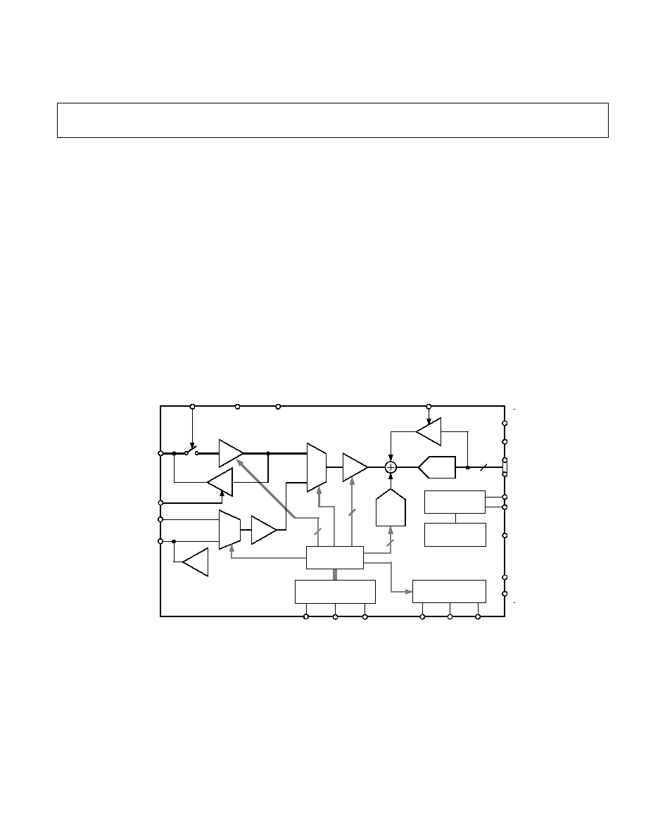
FUNCTIONAL BLOCK DIAGRAM
DATACLK
SHD
SHP
BANDGAP
REFERENCE
2:1
MUX
DOUT
AUX2IN
CLPDM
CCDIN
OFFSET
DAC
PBLK
AUX1IN
VRT
VRB
INTERNAL
TIMING
INTERNAL
BIAS
2dB TO 36dB
AVDD
DVDD
DVSS
AVSS
DRVDD
DRVSS
10
8
CML
DIGITAL
INTERFACE
SDATA
SCK
SL
CLPOB
10
CDS
VGA
CLP
BUF
2:1
MUX
CLP
AD9840A
4dB 6dB
INTERNAL
REGISTERS
CLP
10-BIT
ADC
6
FEATURES
40 MSPS Correlated Double Sampler (CDS)
4 dB
6 dB Variable CDS Gain with 6-Bit Resolution
2 dB to 36 dB 10-Bit Variable Gain Amplifier (VGA)
Low Noise Clamp Circuits
Analog Preblanking Function
10-Bit 40 MSPS A/D Converter
Auxiliary Inputs with VGA and Input Clamp
3-Wire Serial Digital Interface
3 V Single Supply Operation
Low Power: 155 mW @ 3.0 V Supply
48-Lead LQFP Package
APPLICATIONS
Digital Video Camcorders
Digital Still Cameras
Industrial Imaging
PRODUCT DESCRIPTION
The AD9840A is a complete analog signal processor for CCD
applications. It features a 40 MHz single-channel architecture
designed to sample and condition the outputs of interlaced and
progressive scan area CCD arrays. The AD9840A's signal chain
consists of an input clamp, correlated double sampler (CDS),
digitally controlled variable gain amplifier (VGA), black level
clamp, and 10-bit A/D converter. Additional input modes are
provided for processing analog video signals.
The internal registers are programmed through a 3-wire serial
digital interface. Programmable features include gain adjustment,
black level adjustment, input configuration, and power-down modes.
The AD9840A operates from a 3 V power supply, typically
dissipates 155 mW, and is packaged in a 48-lead LQFP.
2
REV. 0
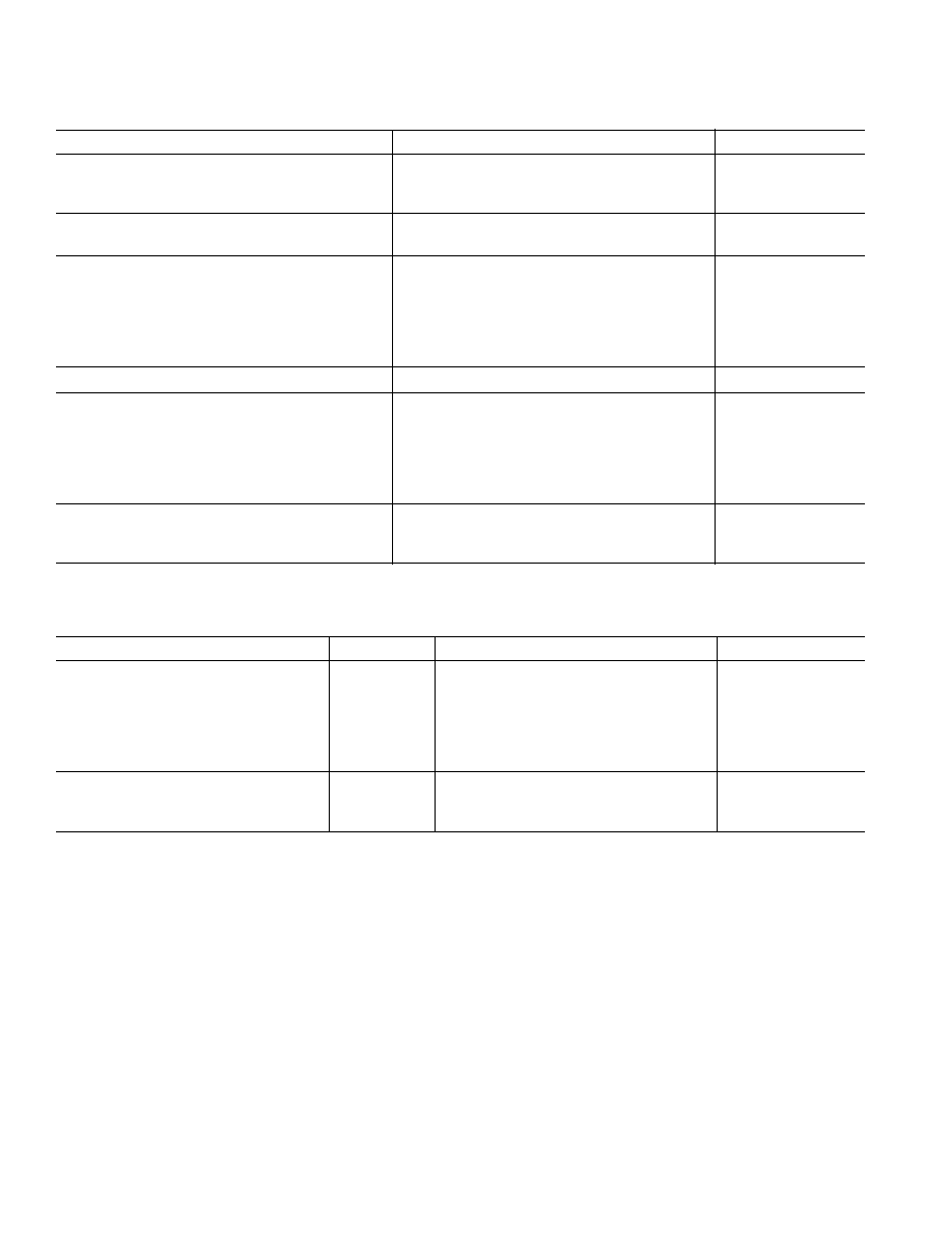
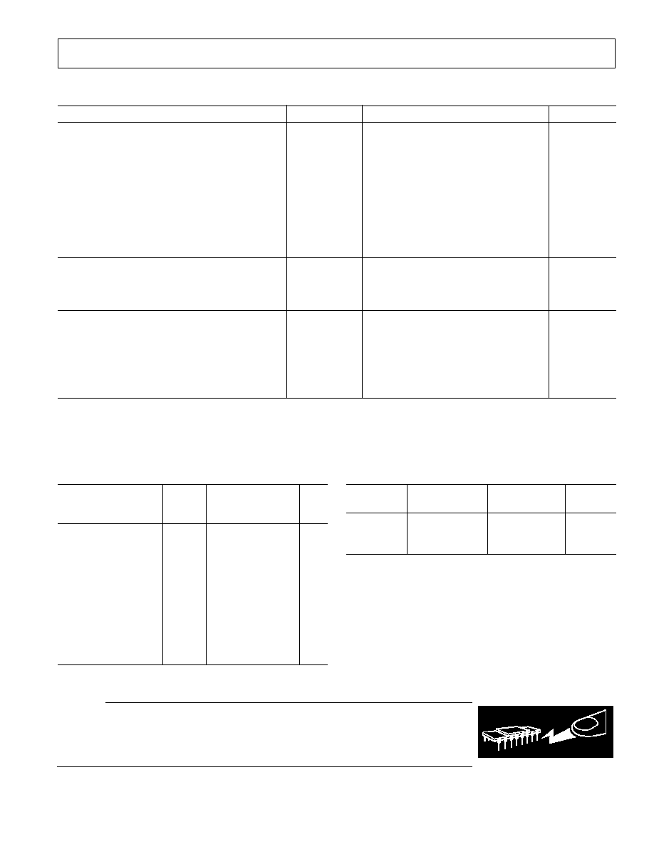
AD9840ASPECIFICATIONS
GENERAL SPECIFICATIONS
Parameter
Min
Typ
Max
Unit
TEMPERATURE RANGE
Operating
20
+85
°C
Storage
65
+150
°C
POWER SUPPLY VOLTAGE
Analog, Digital, Digital Driver
2.7
3.6
V
POWER CONSUMPTION
Normal Operation
(Specified Under Each Mode of Operation)
Power-Down Modes
Fast Recovery Mode
90
mW
Standby
5
mW
Total Power-Down
1
mW
MAXIMUM CLOCK RATE
40
MHz
A/D CONVERTER
Resolution
10
Bits
Differential Nonlinearity (DNL)
±0.5
±1.0
LSB
No Missing Codes
10
Bits Guaranteed
Full-Scale Input Voltage
2.0
V
Data Output Coding
Straight Binary
VOLTAGE REFERENCE
Reference Top Voltage (VRT)
2.0
V
Reference Bottom Voltage (VRB)
1.0
V
Specifications subject to change without notice.
DIGITAL SPECIFICATIONS
Parameter
Symbol
Min
Typ
Max
Unit
LOGIC INPUTS
High Level Input Voltage
V
IH
2.1
V
Low Level Input Voltage
V
IL
0.6
V
High Level Input Current
I
IH
10
µA
Low Level Input Current
I
IL
10
µA
Input Capacitance
C
IN
10
pF
LOGIC OUTPUTS
High Level Output Voltage, I
OH
= 2 mA
V
OH
2.2
V
Low Level Output Voltage, I
OL
= 2 mA
V
OL
0.5
V
Specifications subject to change without notice.
(T
MIN
to T
MAX
, AVDD = DVDD = 3.0 V, f
DATACLK
= 40 MHz, unless otherwise noted.)
(DRVDD = 2.7 V, C
L
= 20 pF unless otherwise noted.)
3
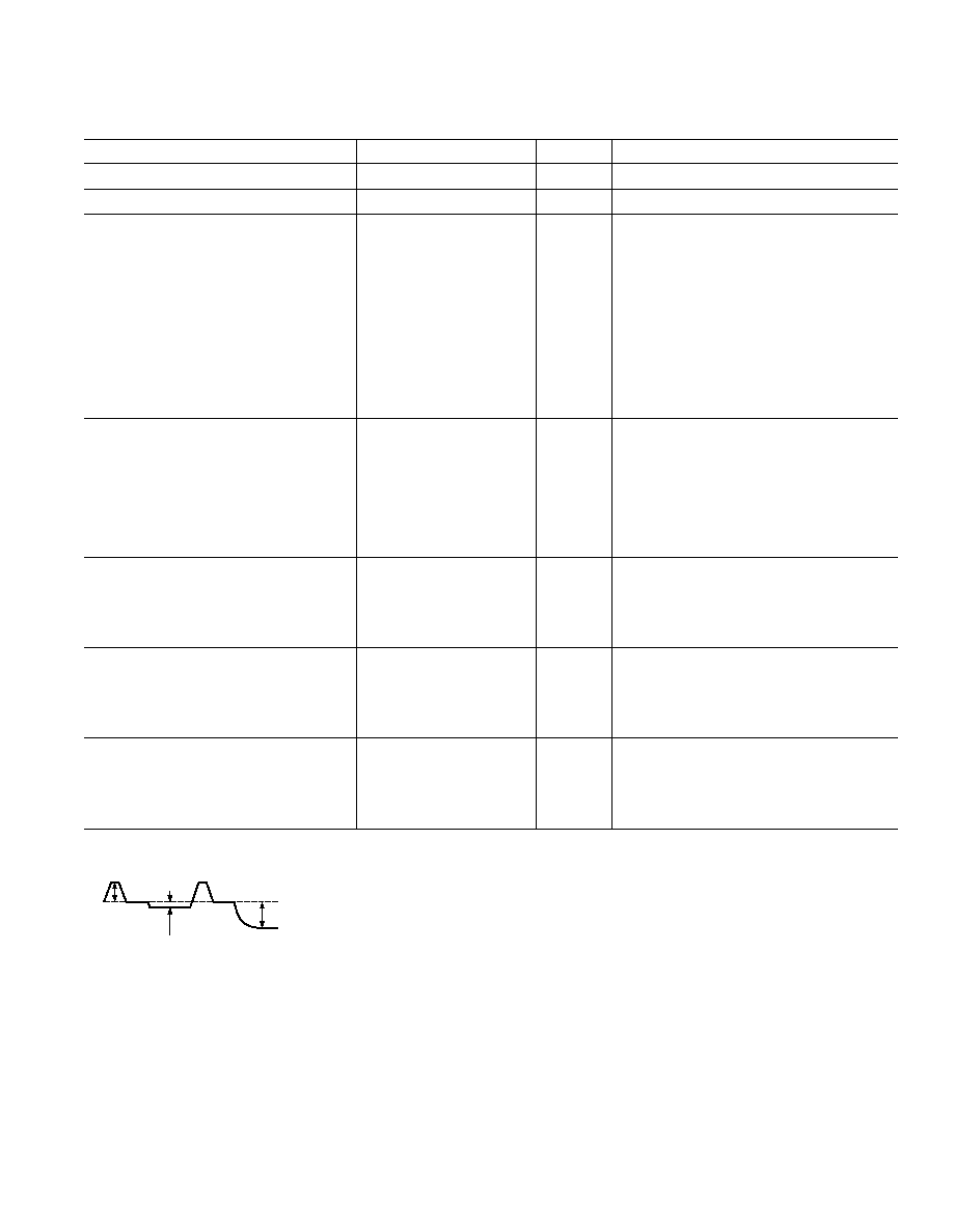
REV. 0
AD9840A
Parameter
Min
Typ
Max
Unit
Notes
P
OWER CONSUMPTION
155
mW
MAXIMUM CLOCK RATE
20
MHz
CDS
Allowable CCD Reset Transient
1
500
mV
See Input Waveform in Note 1
Max CCD Black Pixel Amplitude
1
200
mV
Max Input Range before Saturation
1
1.0
V p-p
With 4 dB CDS Gain
Max Input Range before Saturation
1.5
V p-p
With 2 dB CDS Gain
Max Input Range before Saturation
0.5
V p-p
With 10 dB CDS Gain
Max Output Range
1.6
V p-p
At Any CDS Gain Setting
Gain Resolution
64
Steps
Gain Range (Two's Complement Coding)
See Figure 15 for CDS Gain Curve
Min Gain (CDS Gain Register Code 32)
2
dB
Medium Gain (CDS Gain Code 63)
4
dB
4 dB is Default with CDS Gain Disabled
Max Gain (CDS Gain Code 31)
10
dB
VARIABLE GAIN AMPLIFIER (VGA)
Max Input Range
1.6
V p-p
Max Output Range
2.0
V p-p
Gain Control Resolution
1024
Steps
Gain Monotonicity
Guaranteed
Gain Range
See Figure 13 for VGA
Gain Curve
Low Gain (VGA Register Code 91)
2
dB
See Page 12 for Gain Equations
Max Gain (VGA Code 1023)
36
dB
BLACK LEVEL CLAMP
Clamp Level Resolution
256
Steps
Clamp Level
Measured at ADC Output
Min Clamp Level
0
LSB
Max Clamp Level
63.75
LSB
SYSTEM PERFORMANCE
Specifications Include Entire Signal Chain
Gain Accuracy, VGA Code 91 to 1023
1.0
+1.0
dB
Use Equations on Page 12 to Calculate Gain
Peak Nonlinearity, 500 mV Input Signal
0.4
%
12 dB Gain Applied (4 dB CDS Gain)
Total Output Noise
0.25
LSB rms
AC Grounded Input, 6 dB Gain Applied
Power Supply Rejection (PSR)
40
dB
Measured with Step Change on Supply
POWER-UP RECOVERY TIME
Clocks Must Be Applied, as in Figures 8 and 9
From Fast Recovery Mode
0.1
ms
From Reference Standby Mode
1
ms
From Total Shutdown Mode
3
ms
From Power-Off Condition
15
ms
NOTES
1
Input Signal Characteristics defined as follows, with 4 dB CDS gain:
1V MAX
INPUT
SIGNAL RANGE
200mV MAX
OPTICAL
BLACK PIXEL
500mV TYP
RESET
TRANSIENT
Specifications subject to change without notice.
CCD-MODE SPECIFICATIONS
(T
MIN
to T
MAX
, AVDD = DVDD = 3.0 V, f
DATACLK
= f
SHP
= f
SHD
= 40 MHz, unless otherwise noted.)
4
REV. 0
AD9840ASPECIFICATIONS
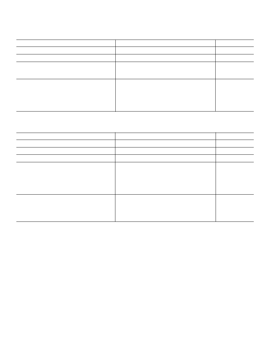
AUX1-MODE SPECIFICATIONS
Parameter
Min
Typ
Max
Unit
POWER CONSUMPTION
105
mW
MAXIMUM CLOCK RATE
40
MHz
INPUT BUFFER
Gain
0
dB
Max Input Range
1.0
V p-p
VGA
Max Output Range
2.0
V p-p
Gain Control Resolution
1023
Steps
Gain (Selected Using VGA Gain Register)
Min Gain
0
dB
Max Gain
36
dB
Specifications subject to change without notice.
AUX2-MODE SPECIFICATIONS
Parameter
Min
Typ
Max
Unit
POWER CONSUMPTION
105
mW
MAXIMUM CLOCK RATE
40
MHz
INPUT BUFFER
(Same as AUX1-MODE)
VGA
Max Output Range
2.0
V p-p
Gain Control Resolution
512
Steps
Gain (Selected Using VGA Gain Register)
Min Gain
0
dB
Max Gain
18
dB
ACTIVE CLAMP
Clamp Level Resolution
256
Steps
Clamp Level (Measured at ADC Output)
Min Clamp Level
0
LSB
Max Clamp Level
63.75
LSB
Specification subject to change without notice.
(T
MIN
to T
MAX
, AVDD = DVDD = 3.0 V, f
DATACLK
= 40 MHz, unless otherwise noted.)
(T
MIN
to T
MAX
, AVDD = DVDD = 3.0 V, f
DATACLK
= 40 MHz, unless otherwise noted.)
AD9840A
5
REV. 0
TIMING SPECIFICATIONS
Parameter
Symbol
Min
Typ
Max
Unit
SAMPLE CLOCKS
DATACLK, SHP, SHD Clock Period
t
CP
25
ns
DATACLK Hi/Low Pulsewidth
t
ADC
10
12.5
ns
SHP Pulsewidth
t
SHP
5
6
ns
SHD Pulsewidth
t
SHD
5
6
ns
CLPDM Pulsewidth
t
CDM
4
10
Pixels
CLPOB Pulsewidth
1
t
COB
2
20
Pixels
SHP Rising Edge to SHD Falling Edge
t
S1
0
6
ns
SHP Rising Edge to SHD Rising Edge
t
S2
10
12.5
ns
Internal Clock Delay
t
ID
3.0
ns
Inhibited Clock Period
t
INH
10
ns
DATA OUTPUTS
Output Delay
t
OD
14.5
16
ns
Output Hold Time
t
H
7.0
7.6
ns
Pipeline Delay
9
Cycles
SERIAL INTERFACE
Maximum SCK Frequency
f
SCLK
10
MHz
SL to SCK Setup Time
t
LS
10
ns
SCK to SL Hold Time
t
LH
10
ns
SDATA Valid to SCK Rising Edge Setup
t
DS
10
ns
SCK Falling Edge to SDATA Valid Hold
t
DH
10
ns
SCK Falling Edge to SDATA Valid Read
t
DV
10
ns
NOTES
1
Minimum CLPOB pulsewidth is for functional operation only. Wider typical pulses are recommended to achieve low noise clamp performance.
Specifications subject to change without notice.
CAUTION
ESD (electrostatic discharge) sensitive device. Electrostatic charges as high as 4000 V readily
accumulate on the human body and test equipment and can discharge without detection. Although
the AD9840A features proprietary ESD protection circuitry, permanent damage may occur on
devices subjected to high-energy electrostatic discharges. Therefore, proper ESD precautions are
recommended to avoid performance degradation or loss of functionality.
(C
L
= 20 pF, f
SAMP
= 40 MHz, CCD-Mode Timing in Figures 5 and 6, AUX-Mode Timing in Figure 7.
Serial Timing in Figures 810.)
ABSOLUTE MAXIMUM RATINGS
With
Respect
Parameter
To
Min
Max
Unit
AVDD1, AVDD2
AVSS
0.3
+3.9
V
DVDD1, DVDD2
DVSS
0.3
+3.9
V
DRVDD
DRVSS
0.3
+3.9
V
Digital Outputs
DRVSS
0.3
DRVDD + 0.3
V
SHP, SHD, DATACLK
DVSS
0.3
DVDD + 0.3
V
CLPOB, CLPDM, PBLK
DVSS
0.3
DVDD + 0.3
V
SCK, SL, SDATA
DVSS
0.3
DVDD + 0.3
V
VRT, VRB, CMLEVEL
AVSS
0.3
AVDD + 0.3
V
BYP1-4, CCDIN
AVSS
0.3
AVDD + 0.3
V
Junction Temperature
150
°C
Lead Temperature
300
°C
(10 sec)
ORDERING GUIDE
Temperature
Package
Package
Model
Range
Description
Option
AD9840AJST 20
°C to +85°C
Thin Plastic
ST-48
Quad Flatpack
(LQFP)
THERMAL CHARACTERISTICS
Thermal Resistance
48-Lead LQFP Package
JA
= 92
°C
WARNING!
ESD SENSITIVE DEVICE
AD9840A
6
REV. 0
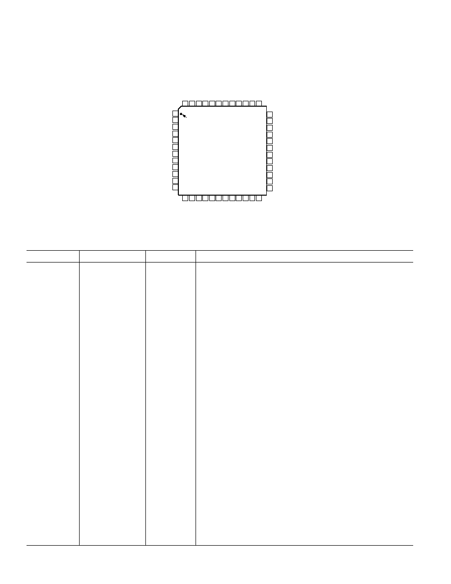
PIN CONFIGURATION
36
35
34
33
32
31
30
29
28
27
26
25
13 14 15 16 17 18 19 20 21 22 23 24
1
2
3
4
5
6
7
8
9
10
11
12
48 47 46 45 44
39 38 37
43 42 41 40
PIN 1
IDENTIFIER
TOP VIEW
(Not to Scale)
AUX1IN
AVSS
AUX2IN
AVDD2
BYP4
NC
CCDIN
DRVSS
DRVSS
(LSB) D0
D1
D2
NC = NO CONNECT
D3
D4
D5
D6
BYP2
BYP1
AVDD1
AVSS
AD9840A
D7
AVSS
SCK
SDATA
SL
NC
STBY
NC
THREE-STATE
DVSS
DVDD2
VRB
VRT
CML
DRVDD
DRVSS
DVSS
DATACLK
DVDD1
DVSS
PBLK
CLPOB
SHP
SHD
CLPDM
DVSS
D8
(MSB) D9
PIN FUNCTION DESCRIPTIONS
Pin Number
Name
Type
Description
1, 2
DRVSS
P
Digital Driver Ground
312
D0D9
DO
Digital Data Outputs
13
DRVDD
P
Digital Output Driver Supply
14
DRVSS
P
Digital Output Driver Ground
15, 18, 24, 41
DVSS
P
Digital Ground
16
DATACLK
DI
Digital Data Output Latch Clock
17
DVDD1
P
Digital Supply
19
PBLK
DI
Preblanking Clock Input
20
CLPOB
DI
Black Level Clamp Clock Input
21
SHP
DI
CDS Sampling Clock for CCD's Reference Level
22
SHD
DI
CDS Sampling Clock for CCD's Data Level
23
CLPDM
DI
Input Clamp Clock Input
25, 26, 35
AVSS
P
Analog Ground
27
AVDD1
P
Analog Supply
28
BYP1
AO
Internal Bias Level. Decoupling
29
BYP2
AO
Internal Bias Level Decoupling
30
CCDIN
AI
Analog Input for CCD Signal
31
NC
NC
Leave Floating or Decouple to Ground with 0.1 F
32
BYP4
AO
Internal Bias Level Decoupling
33
AVDD2
P
Analog Supply
34
AUX2IN
AI
Analog Input
36
AUX1IN
AI
Analog Input
37
CML
AO
Internal Bias Level Decoupling
38
VRT
AO
A/D Converter Top Reference Voltage Decoupling
39
VRB
AO
A/D Converter Bottom Reference Voltage Decoupling
40
DVDD2
P
Digital Supply
42
THREE-STATE
DI
Digital Output Disable. Active High
43
NC
NC
May be tied High or Low. Should not be left floating.
44
STBY
DI
Standby Mode, Active High. Same as Serial Interface Standby Mode
45
NC
NC
Internally Not Connected. May be tied high or low
46
SL
DI
Serial Digital Interface Load Pulse
47
SDATA
DI
Serial Digital Interface Data
48
SCK
DI
Serial Digital Interface Clock
TYPE: AI = Analog Input, AO = Analog Output, DI = Digital Input, DO = Digital Output, P = Power.
AD9840A
7
REV. 0
DEFINITIONS OF SPECIFICATIONS
DIFFERENTIAL NONLINEARITY (DNL)
An ideal ADC exhibits code transitions that are exactly 1 LSB
apart. DNL is the deviation from this ideal value. Thus every code
must have a finite width. No missing codes guaranteed to 10-bit
resolution indicates that all 1024 codes, respectively, must be
present over all operating conditions.
PEAK NONLINEARITY
Peak nonlinearity, a full signal chain specification, refers to the
peak deviation of the output of the AD9840A from a true straight
line. The point used as "zero scale" occurs 1/2 LSB before the
first code transition. "Positive full scale" is defined as a Level
1, 1/2 LSB beyond the last code transition. The deviation is mea-
sured from the middle of each particular output code to the true
straight line. The error is then expressed as a percentage of the 2 V
ADC full-scale signal. The input signal is always appropriately
gained up to fill the ADC's full-scale range.
TOTAL OUTPUT NOISE
The rms output noise is measured using histogram techniques.
The standard deviation of the ADC output codes is calculated
in LSB, and represents the rms noise level of the total signal
chain at the specified gain setting. The output noise can be
converted to an equivalent voltage, using the relationship 1 LSB
= (ADC Full Scale/2
N
codes) when N is the bit resolution of the
ADC. For the AD9840A, 1 LSB is 2 mV.
POWER SUPPLY REJECTION (PSR)
The PSR is measured with a step change applied to the supply
pins. This represents a very high-frequency disturbance on the
AD9840A's power supply. The PSR specification is calculated
from the change in the data outputs for a given step change in
the supply voltage.
INTERNAL DELAY FOR SHP/SHD
The internal delay (also called aperture delay) is the time delay
that occurs from when a sampling edge is applied to the AD9840A
until the actual sample of the input signal is held. Both SHP and
SHD sample the input signal during the transition from low to
high, so the internal delay is measured from each clock's rising
edge to the instant the actual internal sample is taken.
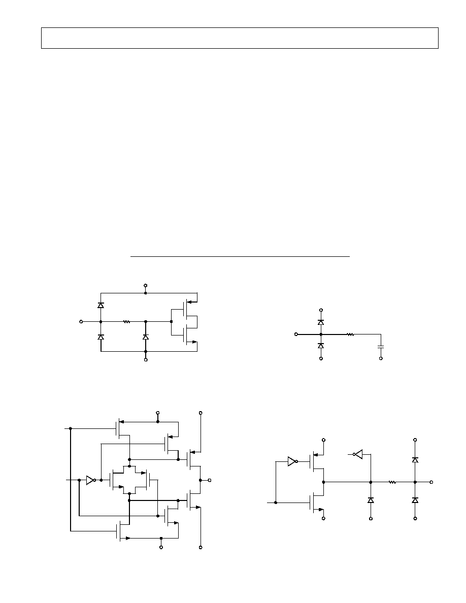
EQUIVALENT INPUT CIRCUITS
330
DVDD
DVSS
Figure 1. Digital Inputs--SHP, SHD, DATACLK, CLPOB,
CLPDM, HD, VD, PBLK, SCK, SL
DVDD
DVSS
DRVSS
DRVDD
THREE-
STATE
DATA
DOUT
Figure 2. Data Outputs
ACVDD
ACVSS
ACVSS
Figure 3. CCDIN (Pin 30)
330
DVDD
DVDD
DVSS
DATA IN
RNW
DATA OUT
DVSS
DVSS
Figure 4. SDATA (Pin 47)
AD9840A
8
REV. 0
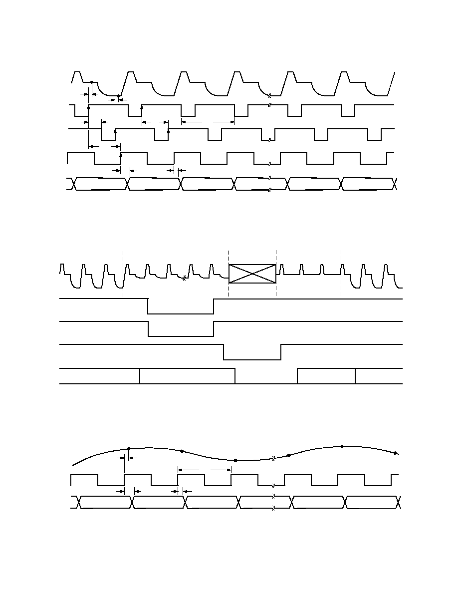
CCD-MODE AND AUX-MODE TIMING
N10
N9
N8
N1
N
N
N+1
N+2
N+9
N+10
t
ID
t
ID
t
S1
t
S2
t
CP
t
INH
t
OD
t
H
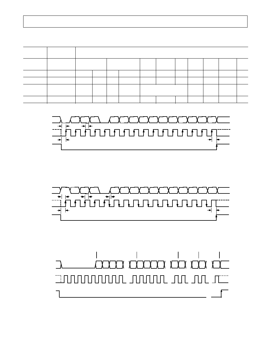
NOTES:
1. RECOMMENDED PLACEMENT FOR DATACLK RISING EDGE IS BETWEEN THE SHD RISING EDGE AND NEXT SHP FALLING EDGE.
2. CCD SIGNAL IS SAMPLED AT SHP AND SHD RISING EDGES.
SHP
SHD
DATACLK
OUTPUT
DATA
CCD
SIGNAL
Figure 5. CCD-Mode Timing
CCD
SIGNAL
EFFECTIVE PIXELS
CLPOB
CLPDM
OPTICAL BLACK PIXELS
HORIZONTAL
BLANKING
DUMMY PIXELS
EFFECTIVE PIXELS
PBLK
NOTES:
1. CLPOB AND CLPDM WILL OVERWRITE PBLK. PBLK WILL NOT AFFECT CLAMP OPERATION IF OVERLAPPING CLPDM AND/OR CLPOB.
2. PBLK SIGNAL IS OPTIONAL.
3. DIGITAL OUTPUT DATA WILL BE ALL ZEROS DURING PBLK. OUTPUT DATA LATENCY IS 9 DATACLK CYCLES.
OUTPUT
DATA
EFFECTIVE PIXEL DATA
OB PIXEL DATA
DUMMY BLACK
EFFECTIVE DATA
Figure 6. Typical CCD-Mode Line Clamp Timing
DATACLK
OUTPUT
DATA
VIDEO
SIGNAL
N
N+1
N+2
N+8
N+9
N10
N9
N8
N1
N
t
ID
t
CP
t
OD
t
H
Figure 7. AUX-Mode Timing
AD9840A
9
REV. 0
SERIAL INTERFACE TIMING AND INTERNAL REGISTER DESCRIPTION
Table I. Internal Register Map
Register
Address
Data Bits
Name
A0
A1 A2
D0
D1
D2
D3
D4
D5
D6
D7
D8
D9
D10
Operation
0
0
0
Channel Select
Power-Down
Software OB Clamp 0
*
1
**
0
*
0
*
0
*
CCD/AUX
Modes
Reset
On/Off
VGA Gain
1
0
0
LSB
MSB
X
Clamp Level
0
1
0
LSB
MSB
X
X
X
Control
1
1
0
0
*
0
*
0
* CDS Gain Clock Polarity Select for
0
*
0
*
Three-
X
On/Off
SHP/SHD/CLP/DATA
State
CDS Gain
0
0
1
LSB
MSB
X
X
X
X
X
*
Internal use only, must be set to zero.
**Should be set to one.
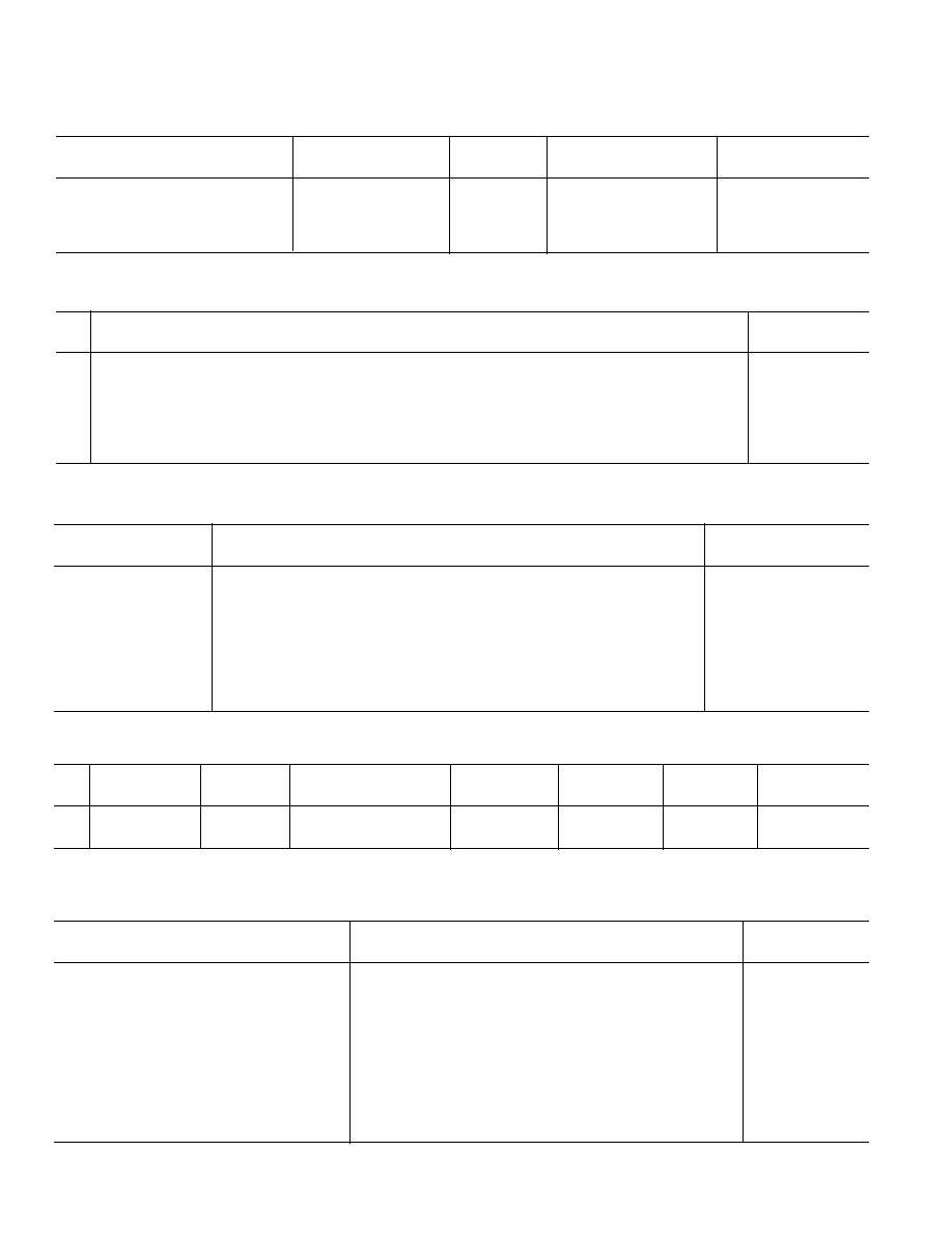
SDATA
SCK
SL
RNW
TEST
0
A2
0
A0
A1
D0
D1
D2
D3
D4
D5
D6
D7
D8
D9
D10
t
DS
t
DH
t
LS
t
LH
NOTES:
1. SDATA BITS ARE INTERNALLY LATCHED ON THE RISING EDGES OF SCK.
2. RNW = READ-NOT WRITE. SET LOW FOR WRITE OPERATION.
3. TEST BIT = INTERNAL USE ONLY. MUST BE SET LOW.
4. SYSTEM UPDATE OF LOADED REGISTERS OCCURS ON SL RISING EDGE.
Figure 8. Serial Write Operation
SDATA
SCK
SL
RNW
TEST
1
0
A0
A1
D0
D1
D2
D3
D4
D5
D6
D7
D8
D9
D10
t
DS
t
DH
t
LS
t
LH
NOTES:
1. RNW = READ-NOT WRITE. SET HIGH FOR READ OPERATION.
2. TEST BITS = INTERNAL USE ONLY. MUST BE SET LOW.
3. SERIAL DATA FROM THE SELECTED REGISTER IS VALID STARTING AFTER THE 5TH SCK FALLING EDGE, AND IS UPDATED ON SCK
FALLING EDGES.
t
DV
A2
Figure 9. Serial Readback Operation
SDATA
SCK
SL
A0
A1
D0
D2
D3
D10
RNW
0
0
D9
0
0
0
D0
1
2
17
35
34
27
26
16
6
5
4
3
44
...
...
...
...
10 BITS
AGC GAIN
D7
D0
D9
...
...
...
...
...
NOTES:
1. ANY NUMBER OF ADJACENT REGISTERS MAY BE LOADED SEQUENTIALLY, BEGINNING WITH THE LOWEST ADDRESS AND INCREMENTING
ONE ADDRESS AT A TIME.
2. WHEN SEQUENTIALLY LOADING MULTIPLE REGISTERS, THE EXACT REGISTER LENGTH (SHOWN ABOVE) MUST BE USED FOR EACH REGISTER.
3. ALL LOADED REGISTERS WILL BE SIMULTANEOUSLY UPDATED WITH THE RISING EDGE OF SL.
8 BITS
CLAMP LEVEL
10 BITS
CONTROL
11 BITS
OPERATION
D1
D0
D2
D3
D1
18
19
20
7
8
9
Figure 10. Continuous Serial Write Operation to Multiple Registers
AD9840A
10
REV. 0
Table II. Operation Register Contents (Default Value x000)
Optical Black Clamp
Reset
Power-Down Modes
Channel Selection
D10
D9
D8
D7
D6
D5
D4
D3 D2
D1 D0
0
*
0
*
0
*
1
**
0
*
0
Enable Clamping
0 Normal
0
0 Normal Power
0
0
CCD-Mode
1
Disable Clamping
1 Reset all
0
1 Fast Recovery
0
1
AUX1-Mode
Registers
1
0 Standby
1
0
AUX2-Mode
to Default
1
1 Total Power-Down 1
1
Test Only
*Must be set to zero. **Set to one.
Table III. VGA Gain Register Contents (Default Value x096)
MSB
LSB
D10
D9
D8
D7
D6
D5
D4
D3
D2
D1
D0
Gain (dB)
X
0
0
0
1
0
1
1
1
1
1
2.0
·
·
·
·
·
·
1
1
1
1
1
1
1
1
1
0
35.965
1
1
1
1
1
1
1
1
1
1
36.0
Table IV. Clamp Level Register Contents (Default Value x080)
MSB
LSB
D10
D9
D8
D7
D6
D5
D4
D3
D2
D1
D0
Clamp Level (LSB)
X
X
X
0
0
0
0
0
0
0
0
0
0
0
0
0
0
0
0
1
0.25
0
0
0
0
0
0
1
0
0.5
·
·
·
·
·
·
1
1
1
1
1
1
1
0
63.5
1
1
1
1
1
1
1
1
63.75
Table V. Control Register Contents (Default Value x000)
Data Out
DATACLK
CLP/PBLK
SHP/SHD
CDS Gain
D10
D9
D8
D7
D6
D5
D4
D3
D2
D1
D0
X
0 Enable
0
*
0
*
0 Rising Edge Trigger
0 Active Low
0 Active Low
0 Disabled
** 0*
0
*
0
*
1 Three-State
1 Falling Edge Trigger
1 Active High
1 Active High
1 Enabled
*Must be set to zero.
**When D3 = 0 (CDS Gain Disabled), the CDS Gain Register is fixed at 4 dB (code 63 dec).
Table VI. CDS Gain Register Contents (Default Value x000)
MSB
LSB
D10
D9
D8
D7
D6
D5
D4
D3
D2
D1
D0
Gain (dB)
*
X
X
X
X
X
0
0
0
0
0
0
+4.3
·
·
·
·
·
·
0
1
1
1
1
0
+10.0
1
0
0
0
0
0
2.0
·
·
·
·
·
·
1
1
1
1
1
1
+4.0
*Control Register Bit D3 must be set high for the CDS Gain Register to be used.
AD9840A
11
REV. 0
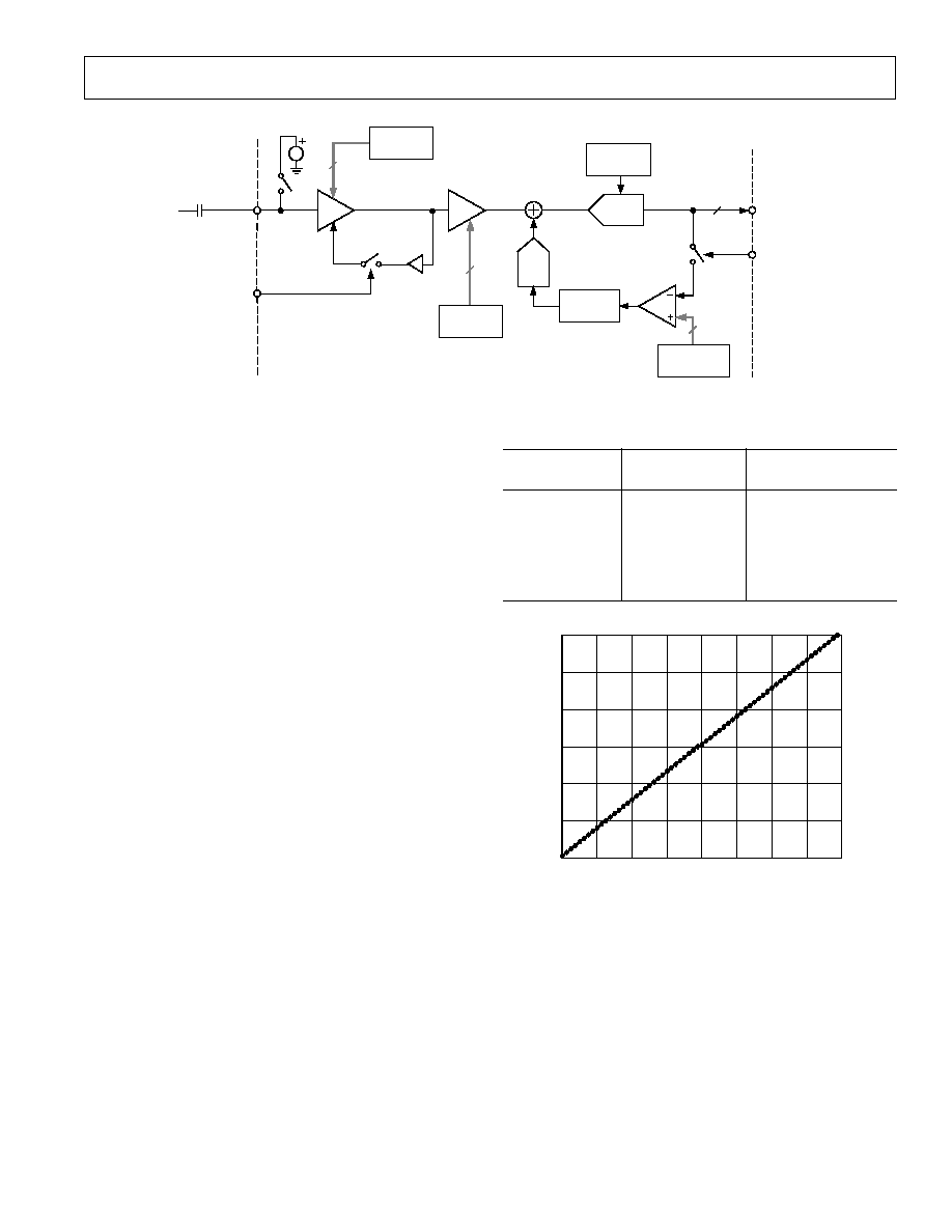
2dB TO 36dB
CLPDM
CCDIN
10
DIGITAL
FILTERING
CLPOB
DC RESTORE
INPUT OFFSET
CLAMP
OPTICAL BLACK
CLAMP
0 TO 64 LSB
0.1 F
DOUT
10-BIT
ADC
VGA
8-BIT
DAC
8
VGA GAIN
REGISTER
10
CDS
2dB TO +10dB
INTERNAL
V
REF
2V FULL SCALE
CDS GAIN
REGISTER
6
CLAMP LEVEL
REGISTER
Figure 11. CCD-Mode Block Diagram
CIRCUIT DESCRIPTION AND OPERATION
The AD9840A signal processing chain is shown in Figure 11.
Each processing step is essential in achieving a high-quality
image from the raw CCD pixel data.
DC Restore
To reduce the large dc offset of the CCD output signal, a
dc-restore circuit is used with an external 0.1
µF series-coupling
capacitor. This restores the dc level of the CCD signal to approxi-
mately 1.5 V, to be compatible with the 3 V single supply of
the AD9840A.
Correlated Double Sampler
The CDS circuit samples each CCD pixel twice to extract the
video information and reject low-frequency noise. The timing
shown in Figure 5 illustrates how the two CDS clocks, SHP
and SHD, are used to sample the reference level and data level
of the CCD signal respectively. The CCD signal is sampled on the
rising edges of SHP and SHD. Placement of these two clock
signals is critical in achieving the best performance from the CCD.
An internal SHP/SHD delay (t
ID
) of 3 ns is caused by internal
propagation delays.
The CDS stage has a default gain of 4 dB, but uses a unique
architecture that allows the CDS gain to be varied. Using the
CDS Gain Register, the gain-of is programmable from 2 dB to
+10 dB in 64 steps, using two's complement coding. The CDS
Gain curve is shown in Figure 12. To change the gain of the
CDS using the CDS Gain Register, the Control Register bit D3
must be set high (CDS Gain Enabled). The default gain setting
when bit Control Register Bit D3 is low (CDS Gain Disabled) is
4 dB. See Tables V and VI for more details.
A CDS gain of 4 dB provides some front-end signal gain and
improves the overall signal-to-noise ratio. This gain setting
works very well in most applications, and the CCD-Mode
Specifications use this default gain setting. However, the CDS
gain may be varied to optimize the AD9840A operation in a
particular application. Increased CDS gain can be useful with
low output level CCDs, while decreased CDS gain allows the
AD9840A to accept CCD signal swings greater than 1 V p-p.
Table VII summarizes some example CDS gain settings for
different maximum signal swings. The CDS Gain Register may
also be used "on the fly" to provide a +6 dB boost or 6 dB
attenuation when setting exposure levels. It is best to keep the
CDS output level from exceeding 1.5 V1.6 V.
Table VII. Example CDS Gain Settings
Recommended
Max Input Signal
Gain Range
Register Code Range
250 mV p-p
8 dB to 10 dB
21 to 31
500 mV p-p
6 dB to 8 dB
10 to 21
800 mV p-p
4 dB to 6 dB
63 to 10
1 V p-p
2 dB to 4 dB
53 to 63
1.25 V p-p
0 dB to 2 dB
42 to 53
1.5 V p-p
2 dB to 0 dB
32 to 42
CDS GAIN REGISTER CODE
10
32
CDS GAIN
dB
40
48
56
0
8
16
24
31
8
6
4
2
0
-2
(100000)
(011111)
Figure 12. CDS Gain Curve
Input Clamp
A line-rate input clamping circuit is used to remove the CCD's
optical black offset. This offset exists in the CCD's shielded
black reference pixels. Unlike some AFE architectures, the
AD9840A removes this offset in the input stage to minimize the
effect of a gain change on the system black level, usually called the
"gain step." Another advantage of removing this offset at the
input stage is to maximize system headroom. Some area CCDs
have large black level offset voltages, which, if not corrected at
the input stage, can significantly reduce the available headroom
in the internal circuitry when higher VGA gain settings are used.
Horizontal timing is shown in Figure 6. It is recommended
that the CLPDM pulse be used during valid CCD dark pixels.
CLPDM may be used during the optical black pixels, either
AD9840A
12
REV. 0
together with CLPOB or separately. The CLPDM pulse should
be a minimum of four pixels wide.
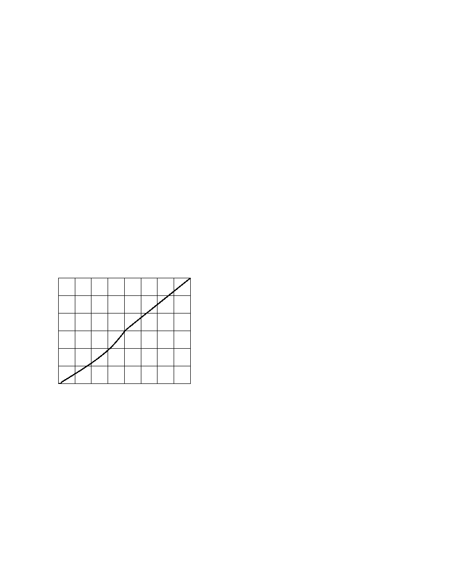
Variable Gain Amplifier
The VGA stage provides a gain range of 2 dB to 36 dB, program-
mable with 10-bit resolution through the serial digital interface.
Combined with the typical 4 dB gain from the CDS
stage, the
total gain range for the AD9840A is 6 dB to 40 dB. A gain of 6 dB
will match a 1 V input signal with the ADC full-scale range of 2 V.
When compared to 1 V full-scale systems (such as ADI's AD9803),
the equivalent gain range is 0 dB to 34 dB.
The VGA gain curve is divided into two separate regions. When
the VGA Gain Register code is between 0 and 511, the curve
follows a (1 + x)/(1 x) shape, which is similar to a "linear-in-
dB" characteristic. From code 512 to code 1023, the curve follows
a "linear-in-dB" shape. The exact VGA gain can be calculated
for any Gain Register value by using the following two equations:
Code Range
Gain Equation (dB)
0511
Gain = 20 log
10
([658 + code]/[658 code]) 0.35
5121023
Gain = (0.0354)(code) 0.35
Using these two equations, the actual gain of the AD9840A can
be accurately predicted to within 0.5 dB. As shown in the CCD-
Mode Specifications, only the VGA gain range from 2 dB to 36 dB
is specified. This corresponds to a VGA gain code range of 91 to
1023. The Gain Accuracy specifications also include a CDS gain
of 4 dB, for a total gain range of 6 dB to 40 dB.
VGA GAIN REGISTER CODE
36
0
VGA GAIN
dB
127
255
383
511
639
767
895
1023
30
24
18
12
6
0
Figure 13. VGA Gain Curve (Gain from CDS Not Included)
Optical Black Clamp
The optical black clamp loop is used to remove residual offsets
in the signal chain, and to track low-frequency variations in the
CCD's black level. During the optical black (shielded) pixel
interval on each line, the ADC output is compared with a fixed
black level reference, selected by the user in the Clamp Level
Register. Any value between 0 LSB and 64 LSB may be pro-
grammed, with 8-bit resolution. The resulting error signal is
filtered to reduce noise, and the correction value is applied to
the ADC input through a D/A converter. Normally, the optical
black clamp loop is turned on once per horizontal line, but this
loop can be updated more slowly to suit a particular application.
If external digital clamping is used during the post processing, the
AD9840A's optical black clamping may be disabled using Bit D5
in the Operation Register (see Serial Interface Timing and
Internal Register Description section). When the loop is dis-
abled, the Clamp Level Register may still be used to provide
programmable offset adjustment.
Horizontal timing is shown in Figure 6. The CLPOB pulse
should be placed during the CCD's optical black pixels. It is
recommended that the CLPOB pulse duration be at least 20
pixels wide to minimize clamp noise. Shorter pulsewidths may be
used, but clamp noise may increase, and the loop's ability to
track low-frequency variations in the black level will be reduced.
A/D Converter
The AD9840A uses a high-performance ADC architecture,
optimized for high speed and low power. Differential nonlin-
earity (DNL) performance is typically better than 0.5 LSB.
Instead of the 1 V full-scale range used by the earlier AD9801 and
AD9803 products from Analog Devices, the AD9840A's ADC
uses a 2 V input range. Better noise performance results from
using a larger ADC full-scale range.
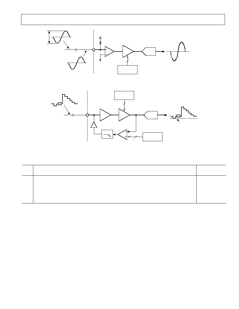
AUX1-Mode
For applications that do not require CDS, the AD9840A can be
configured to sample ac-coupled waveforms. Figure 14 shows the
circuit configuration for using the AUX1 channel input (Pin
36). A single 0.1
µF ac-coupling capacitor is needed between the
input signal driver and the AUX1IN pin. An on-chip dc-bias
circuit sets the average value of the input signal to approxi-
mately 0.4 V, which is referenced to the midscale code of the ADC.
The VGA gain register provides a gain range of 0 dB to 36 dB
in this mode of operation (see VGA Gain Curve, Figure 13).
The VGA gains up the signal level with respect to the 0.4 V bias
level. Signal levels above the bias level will be further increased
to a higher ADC code, while signal levels below the bias level
will be further decreased to a lower ADC code.
AUX2-Mode
For sampling video-type waveforms, such as NTSC and PAL
signals, the AUX2 channel provides black level clamping, gain
adjustment, and A/D conversion. Figure 15 shows the circuit
configuration for using the AUX2 channel input (Pin 34). An
external 0.1
µF blocking capacitor is used with the on-chip
video clamp circuit, to level-shift the input signal to a desired
reference level. The clamp circuit automatically senses the most
negative portion of the input signal, and adjusts the voltage
across the input capacitor. This forces the black level of the input
signal to be equal to the value programmed into the Clamp Level
register (see Serial Interface Register Description). The VGA
provides gain adjustment from 0 dB to 18 dB. The same VGA
Gain register is used, but only the 9 MSBs of the gain register
are used (see Table VIII.)
AD9840A
13
REV. 0
Table VIII. VGA Gain Register Used for AUX2-Mode
MSB
LSB
D10
D9
D8
D7
D6
D5
D4
D3
D2
D1
D0
Gain (dB)
X
0
X
X
X
X
X
X
X
X
X
0.0
1
0
0
0
0
0
0
0
0
0
0.0
·
·
·
·
·
·
1
1
1
1
1
1
1
1
1
1
18.0
AUX1IN
0.1 F
VGA GAIN
REGISTER
ADC
VGA
10
5k
0.4V
0.4V
INPUT SIGNAL
??V
0.8V
0.4V
MIDSCALE
0dB TO 36dB
Figure 14. AUX1 Circuit Configuration
0dB TO 18dB
8
AUX2IN
BUFFER
0.1 F
VIDEO
SIGNAL
9
CLAMP LEVEL
LPF
VGA GAIN
REGISTER
ADC
VGA
VIDEO CLAMP
CIRCUIT
CLAMP LEVEL
REGISTER
Figure 15. AUX2 Circuit Configuration
AD9840A
14
REV. 0
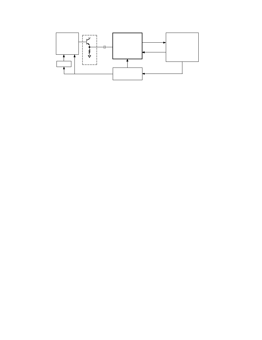
APPLICATIONS INFORMATION
The AD9840A is a complete Analog Front End (AFE) product
for digital still camera and camcorder applications. As shown in
Figure 16, the CCD image (pixel) data is buffered and sent to
the AD9840A analog input through a series input capacitor. The
AD9840A performs the dc restoration, CDS, gain adjustment,
black level correction, and analog-to-digital conversion. The
AD9840A's digital output data is then processed by the image
processing ASIC. The internal registers of the AD9840A--used
to control gain, offset level, and other functions--are programmed
by the ASIC or microprocessor through a 3-wire serial digital
interface. A system timing generator provides the clock signals
for both the CCD and the AFE.
Internal Power-On Reset Circuitry
After power-on, the AD9840A will automatically reset all internal
registers and perform internal calibration procedures. This takes
approximately 1 ms to complete. During this time, normal clock
signals and serial write operations may occur. However, serial
register writes will be ignored until the internal reset operation is
completed. Pin 43 (formerly RSTB on the AD9843 non-A) is no
longer used for the reset operation. Toggling Pin 43 in the
AD9840A will have no effect.
CCD
CCDIN
BUFFER
V
OUT
0.1 F
ADC
OUT
REGISTER
DATA
SERIAL
INTERFACE
DIGITAL
OUTPUTS
DIGITAL IMAGE
PROCESSING
ASIC
TIMING
GENERATOR
V-DRIVE
CCD
TIMING
CDS/CLAMP
TIMING
AD9840A
Figure 16. System Applications Diagram
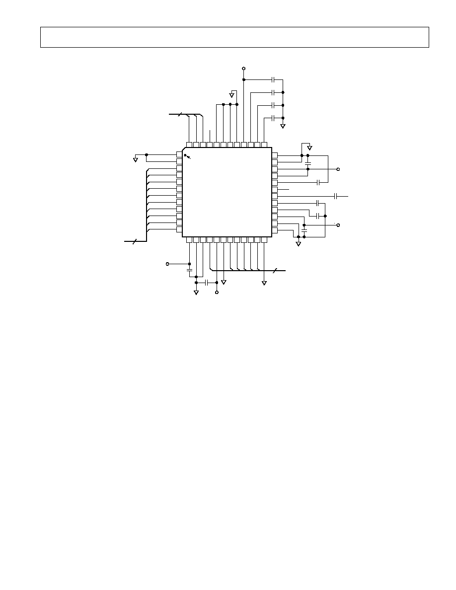
Grounding and Decoupling Recommendations
As shown in Figure 17, a single ground plane is recommended
for the AD9840A. This ground plane should be as continuous
as possible, particularly around Pins 25 through 39. This will
ensure that all analog decoupling capacitors provide the lowest
possible impedance path between the power and bypass pins
and their respective ground pins. All decoupling capacitors
should be located as close as possible to the package pins. A
single clean power supply is recommended for the AD9840A,
but a separate digital driver supply may be used for DRVDD
(Pin 13). DRVDD should always be decoupled to DRVSS (Pin
14), which should be connected to the analog ground plane.
Advantages of using a separate digital driver supply include
using a lower voltage (2.7 V) to match levels with a 2.7 V ASIC,
reducing digital power dissipation, and reducing potential noise
coupling. If the digital outputs (Pins 312) must drive a load
larger than 20 pF, buffering is recommended to reduce digital
code transition noise. Alternatively, placing series resistors
close to the digital output pins may help reduce noise.
AD9840A
15
REV. 0
DRVDD
DRVSS
DVSS
DATACLK
DVDD1
DVSS
PBLK
CLPOB
SHP
SHD
CLPDM
DVSS
13 14 15 16 17 18 19 20 21 22 23 24
1
2
3
4
5
6
7
8
9
10
11
12
37
48 47 46 45 44
39 38
43 42 41 40
PIN 1
IDENTIFIER
TOP VIEW
(Not to Scale)
AD9840A
36
35
34
33
32
31
30
29
28
27
26
25
AUX1IN
AVSS
AUX2IN
AVDD2
BYP4
NC
CCDIN
BYP2
BYP1
AVDD1
AVSS
AVSS
DRVSS
DRVSS
(LSB) D0
D1
D2
D3
D4
D5
D6
D7
D8
(MSB) D9
SCK
SDATA
SL
NC
STBY
NC
THREE-STATE
DVSS
DVDD2
VRB
VRT
CML
0.1 F
0.1 F
0.1 F
0.1 F
0.1 F
0.1 F
3V
ANALOG
SUPPLY
CCD
SIGNAL
3V
ANALOG
SUPPLY
10
DATA
OUTPUTS
3
SERIAL
INTERFACE
0.1 F
1.0 F
1.0 F
0.1 F
3V
ANALOG SUPPLY
6
CLOCK
INPUTS
0.1 F
0.1 F
3V
ANALOG SUPPLY
3V
DRIVER
SUPPLY
NC = NO CONNECT
Figure 17. Recommended Circuit Configuration for CCD-Mode
16
C02196010/00 (rev. 0)
PRINTED IN U.S.A.
AD9840A
REV. 0
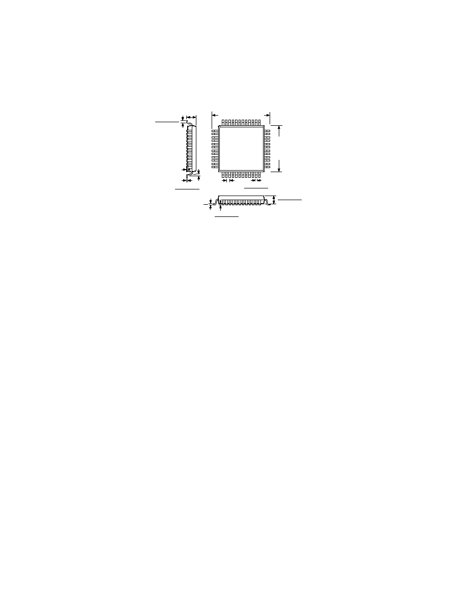
OUTLINE DIMENSIONS
Dimensions shown in inches and (mm).
48-Lead LQFP
(ST-48)
TOP VIEW
(PINS DOWN)
1
12
13
25
24
36
37
48
0.019 (0.5)
BSC
0.276
(7.00)
BSC
SQ
0.011 (0.27)
0.006 (0.17)
0.354 (9.00) BSC SQ
0.063 (1.60)
MAX
0.030 (0.75)
0.018 (0.45)
0.008 (0.2)
0.004 (0.09)
0
MIN
COPLANARITY
0.003 (0.08)
SEATING
PLANE
0.006 (0.15)
0.002 (0.05)
7
0
0.057 (1.45)
0.053 (1.35)
Document Outline
- Specifications
- Pinout
- Package Drawings
- Ordering Guide
- Features
- Applications
- Product Description
- Absolute Maximum Ratings
- Functional Block Diagram
- Pin Function Description
- CIRCUIT DESCRIPTION
- CAUTION
- DEFINITIONS OF SPECIFICATIONS DIFFERENTIAL NONLINEARITY (DNL)
- POWER SUPPLY REJECTION (PSR)
- PEAK NONLINEARITY
- INTERNAL DELAY FOR SHP/SHD
- TOTAL OUTPUT NOISE
- EQUIVALENT INPUT CIRCUITS
- CCD-MODE AND AUX-MODE TIMING
- SERIAL INTERFACE TIMING AND INTERNAL REGISTER DESCRIPTION
- DIAGRAMS
- Digital InputsSHP, SHD, DATACLK, CLPOB, CLPDM, HD, VD, PBLK, SCK, SL
- Data Outputs
- CCDIN (Pin 30)
- SDATA (Pin 47)
- CCD-Mode Timing
- Typical CCD-Mode Line Clamp Timing
- AUX-Mode Timing
- Serial Write Operation
- Serial Readback Operation
- Continuous Serial Write Operation to Multiple Registers
- CCD-Mode Block Diagram
- AUX2 Circuit Configuration
- System Applications Diagram
- Recommended Circuit Configuration for CCD-Mode