AD9832 Data Sheet
REV. A
Information furnished by Analog Devices is believed to be accurate and
reliable. However, no responsibility is assumed by Analog Devices for its
use, nor for any infringements of patents or other rights of third parties
which may result from its use. No license is granted by implication or
otherwise under any patent or patent rights of Analog Devices.
a
AD9832
One Technology Way, P.O. Box 9106, Norwood, MA 02062-9106, U.S.A.
Tel: 781/329-4700
World Wide Web Site: http://www.analog.com
Fax: 781/326-8703
© Analog Devices, Inc., 1999
CMOS
Complete DDS
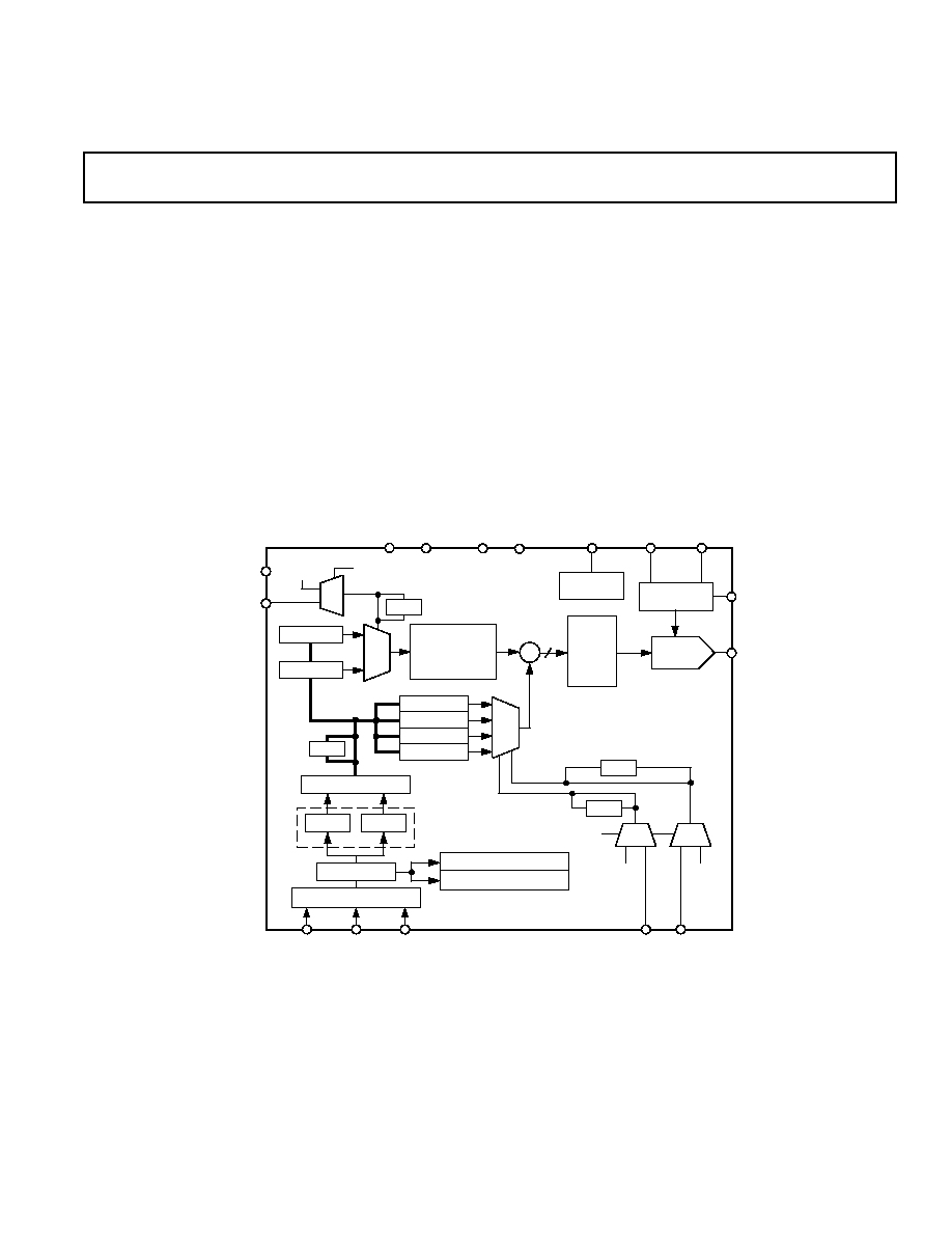
FUNCTIONAL BLOCK DIAGRAM
IOUT
COMP
REFIN
FS ADJUST
REFOUT
AGND
AVDD
DGND
DVDD
MCLK
PSEL0 PSEL1
12
AD9832
ON-BOARD
REFERENCE
10-BIT DAC
PHASE0 REG
PHASE1 REG
PHASE2 REG
PHASE3 REG
FULL-SCALE
CONTROL
SIN
ROM
PHASE
ACCUMULATOR
(32 BIT)
MUX
FREQ0 REG
FREQ1 REG
MUX
16-BIT DATA REGISTER
SYNC
FSELECT
FSELECT
BIT
SELSRC
SYNC
8 LSBs
8 MSBs
DECODE LOGIC
FSYNC
SCLK
SDATA
SERIAL REGISTER
CONTROL REGISTER
FSELECT/PSEL REGISTER
DEFER REGISTER
SYNC
SYNC
SELSRC
PSEL0
BIT
PSEL1
BIT
FEATURES
3 V/5 V Power Supply
25 MHz Speed
On-Chip SINE Look-Up Table
On-Chip 10-Bit DAC
Serial Loading
Power-Down Option
45 mW Power Consumption
16-Lead TSSOP
APPLICATIONS
DDS Tuning
Digital Demodulation
GENERAL DESCRIPTION
The AD9832 is a numerically controlled oscillator employing
a phase accumulator, a sine look-up table and a 10-bit D/A
converter integrated on a single CMOS chip. Modulation
capabilities are provided for phase modulation and frequency
modulation.
Clock rates up to 25 MHz are supported. Frequency accuracy
can be controlled to one part in 4 billion. Modulation is effected
by loading registers through the serial interface.
A power-down bit allows the user to power down the AD9832
when it is not in use, the power consumption being reduced to
5 mW (5 V) or 3 mW (3 V). The part is available in a 16-lead
TSSOP package.
2
REV. A
AD9832SPECIFICATIONS
1
(V
DD
= +3.3 V 10%; +5 V 10%; AGND = DGND = 0 V; T
A
= T
MIN
to T
MAX
; REFIN =
REFOUT; R
SET
= 3.9 k
; R
LOAD
= 300 for IOUT unless otherwise noted)
Parameter
AD9832B
Units
Test Conditions/Comments
SIGNAL DAC SPECIFICATIONS
Resolution
10
Bits
Update Rate (f
MAX
)
25
MSPS nom
I
OUT
Full Scale
4
mA
nom
4.5
mA max
Output Compliance
1.35
V max
3 V Power Supply
DC Accuracy
Integral Nonlinearity
±
1
LSB typ
Differential Nonlinearity
±
0.5
LSB typ
DDS SPECIFICATIONS
2
Dynamic Specifications
Signal to Noise Ratio
50
dB min
f
MCLK
= 25 MHz, f
OUT
= 1 MHz
Total Harmonic Distortion
53
dBc max
f
MCLK
= 25 MHz, f
OUT
= 1 MHz
Spurious Free Dynamic Range (SFDR)
3
f
MCLK
= 6.25 MHz, f
OUT
= 2.11 MHz
Narrow Band (
±
50 kHz)
72
dBc min
5 V Power Supply
70
dBc min
3 V Power Supply
Wide Band (
±
2 MHz)
50
dBc min
Clock Feedthrough
60
dBc typ
Wake-Up Time
4
1
ms typ
Power-Down Option
Yes
VOLTAGE REFERENCE
Internal Reference @ +25
°
C
1.21
Volts typ
T
MIN
to T
MAX
1.21
±
7%
Volts min/max
REFIN Input Impedance
10
M
typ
Reference TC
100
ppm/
°
C typ
REFOUT Output Impedance
300
typ
LOGIC INPUTS
V
INH
, Input High Voltage
V
DD
0.9
V
min
V
INL
, Input Low Voltage
0.9
V
max
I
INH
, Input Current
10
µ
A
max
C
IN
, Input Capacitance
10
pF
max
POWER SUPPLIES
AVDD
2.97/5.5
V
min/V
max
DVDD
2.97/5.5
V
min/V
max
I
AA
5
mA
max
5 V Power Supply
I
DD
2.5 + 0.4/MHz
mA typ
5 V Power Supply
I
AA
+ I
DD
5
15
mA
max
3 V Power Supply
24
mA
max
5 V Power Supply
Low Power Sleep Mode
350
µ
A max
NOTES
1
Operating temperature range is as follows: B Version, 40
°
C to +85
°
C.
2
100% production tested.
3
f
MCLK
= 6.25 MHz, Frequency Word = 5671C71C HEX, f
OUT
= 2.11 MHz.
4
See Figure 11. To reduce the wake-up time at low power supplies and low temperature, the use of an external reference is suggested.
5
Measured with the digital inputs static and equal to 0 V or DVDD.
The AD9832 is tested with a capacitive load of 50 pF. The part can be operated with higher capacitive loads, but the magnitude of the analog output will be attenuated.
For example, a 5 MHz output signal will be attenuated by 3 dB when the load capacitance equals 85 pF.
Specifications subject to change without notice.
IOUT
COMP
REFIN
FS
ADJUST
REFOUT
12
AD9832
ON-BOARD
REFERENCE
10-BIT DAC
SIN
ROM
FULL-SCALE
CONTROL
300
50pF
R
SET
3.9k
10nF
10nF
AVDD
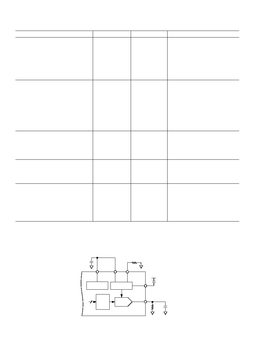
Figure 1. Test Circuit with Which Specifications Are Tested
3
AD9832
REV. A
TIMING CHARACTERISTICS
(V
DD
= +3.3 V
10%; +5 V 10%; AGND = DGND = 0 V, unless otherwise noted)
Limit at
T
MIN
to T
MAX
Parameter
(B Version)
Units
Test Conditions/Comments
t
1
40
ns min
MCLK Period
t
2
16
ns min
MCLK High Duration
t
3
16
ns min
MCLK Low Duration
t
4
50
ns min
SCLK Period
t
5
20
ns min
SCLK High Duration
t
6
20
ns min
SCLK Low Duration
t
7
15
ns min
FSYNC to SCLK Falling Edge Setup Time
t
8
20
ns min
FSYNC to SCLK Hold Time
SCLK 5
ns max
t
9
15
ns min
Data Setup Time
t
10
5
ns min
Data Hold Time
t
11
8
ns min
FSELECT, PSEL0, PSEL1 Setup Time Before MCLK Rising Edge
t
11A
*
8
ns min
FSELECT, PSEL0, PSEL1 Setup Time After MCLK Rising Edge
*See Pin Function Descriptions.
Guaranteed by design but not production tested.
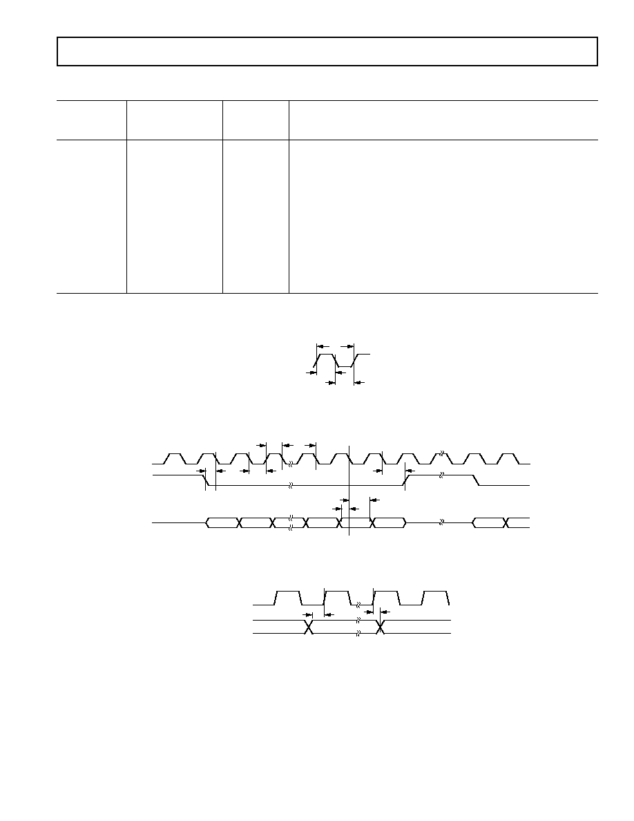
MCLK
t
2
t
1
t
3
Figure 2. Master Clock
SCLK
FSYNC
SDATA
t
5
t
4
t
6
t
7
t
8
t
10
t
9
D15
D14
D2
D1
D0
D15
D14
Figure 3. Serial Timing
t
11A
t
11
VALID DATA
VALID DATA
VALID DATA
MCLK
FSELECT
PSEL0, PSEL1
Figure 4. Control Timing
AD9832
4
REV. A
ABSOLUTE MAXIMUM RATINGS*
(T
A
= +25
°
C unless otherwise noted)
AVDD to AGND . . . . . . . . . . . . . . . . . . . . . . 0.3 V to +7 V
DVDD to DGND . . . . . . . . . . . . . . . . . . . . . . 0.3 V to +7 V
AVDD to DVDD . . . . . . . . . . . . . . . . . . . . 0.3 V to +0.3 V
AGND to DGND. . . . . . . . . . . . . . . . . . . . . 0.3 V to +0.3 V
Digital I/O Voltage to DGND . . . . 0.3 V to DVDD + 0.3 V
Analog I/O Voltage to AGND . . . . . 0.3 V to AVDD + 0.3 V
Operating Temperature Range
Industrial (B Version) . . . . . . . . . . . . . . . 40
°
C to +85
°
C
Storage Temperature Range . . . . . . . . . . . . 65
°
C to +150
°
C
Maximum Junction Temperature . . . . . . . . . . . . . . . +150
°
C
TSSOP
JA
Thermal Impedance . . . . . . . . . . . . . . . 158
°
C/W
Lead Temperature, Soldering
Vapor Phase (60 sec) . . . . . . . . . . . . . . . . . . . . . . . +215
°
C
Infrared (15 sec) . . . . . . . . . . . . . . . . . . . . . . . . . . . +220
°
C
ESD Rating . . . . . . . . . . . . . . . . . . . . . . . . . . . . . . . > 4500 V
*Stresses above those listed under Absolute Maximum Ratings may cause perma-
nent damage to the device. This is a stress rating only; functional operation of the
device at these or any other conditions above those listed in the operational
sections of this specification is not implied. Exposure to absolute maximum rating
conditions for extended periods may affect device reliability.
ORDERING GUIDE
Temperature
Package
Package
Model
Range
Description
Option*
AD9832BRU
40
°
C to +85
°
C
16-Lead TSSOP
RU-16
*RU = Thin Shrink Small Outline Package (TSSOP).
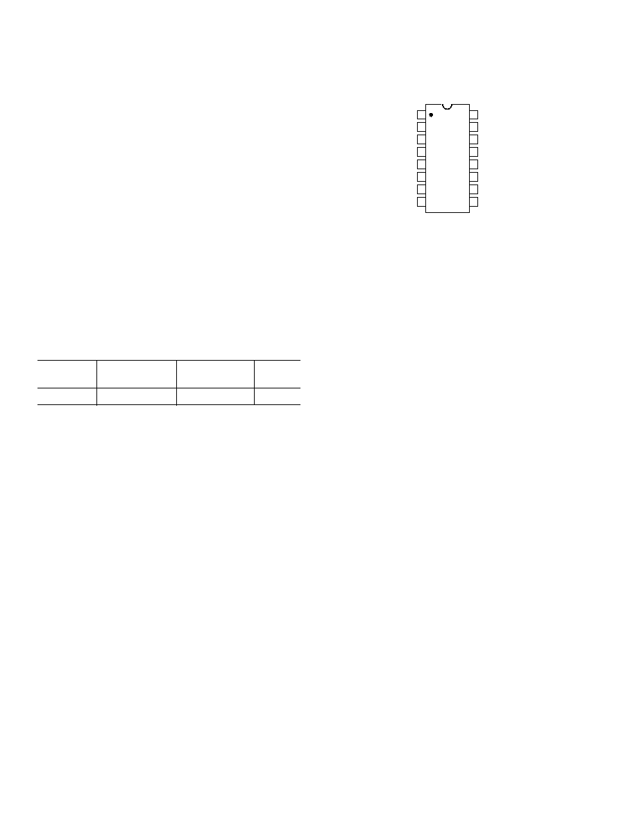
PIN CONFIGURATION
14
13
12
11
16
15
10
9
8
1
2
3
4
7
6
5
TOP VIEW
(Not to Scale)
AD9832
FS ADJUST
AGND
IOUT
AVDD
COMP
REFIN
REFOUT
DVDD
FSELECT
PSEL1
PSEL0
DGND
MCLK
SCLK
SDATA
FSYNC

5
AD9832
REV. A
PIN FUNCTION DESCRIPTIONS
Pin #
Mnemonic
Function
ANALOG SIGNAL AND REFERENCE
1
FS ADJUST
Full-Scale Adjust Control. A resistor (R
SET
) is connected between this pin and AGND. This determines
the magnitude of the full-scale DAC current. The relationship between R
SET
and the full-scale current is
as follows:
IOUT
FULL-SCALE
= 12.5
×
V
REFIN
/R
SET
V
REFIN
= 1.21 V nominal, R
SET
= 3.9 k
typical
2
REFIN
Voltage Reference Input. The AD9832 can be used with either the onboard reference, which is available
from pin REFOUT, or an external reference. The reference to be used is connected to the REFIN pin.
The AD9832 accepts a reference of 1.21 V nominal.
3
REFOUT
Voltage Reference Output. The AD9832 has an onboard reference of value 1.21 V nominal. The refer-
ence is made available on the REFOUT pin. This reference is used as the reference to the DAC by con-
necting REFOUT to REFIN. REFOUT should be decoupled with a 10 nF capacitor to AGND.
14
IOUT
Current Output. This is a high impedance current source. A load resistor should be connected between
IOUT and AGND.
16
COMP
Compensation pin. This is a compensation pin for the internal reference amplifier. A 10 nF decoupling
ceramic capacitor should be connected between COMP and AVDD.
POWER SUPPLY
4
DVDD
Positive Power Supply for the Digital Section. A 0.1
µ
F decoupling capacitor should be connected be-
tween DVDD and DGND. DVDD can have a value of +5 V
±
10% or +3.3 V
±
10%.
5
DGND
Digital Ground.
13
AGND
Analog Ground.
15
AVDD
Positive Power Supply for the Analog Section. A 0.1
µ
F decoupling capacitor should be connected be-
tween AVDD and AGND. AVDD can have a value of +5 V
±
10% or +3.3 V
±
10%.
DIGITAL INTERFACE AND CONTROL
6
MCLK
Digital Clock Input. DDS output frequencies are expressed as a binary fraction of the frequency of MCLK.
The output frequency accuracy and phase noise are determined by this clock.
7
SCLK
Serial Clock, Logic Input. Data is clocked into the AD9832 on each falling SCLK edge.
8
SDATA
Serial Data In, Logic Input. The 16-bit serial data word is applied to this input.
9
FSYNC
Data Synchronization Signal, Logic Input. When this input is taken low, the internal logic is informed
that a new word is being loaded into the device.
10
FSELECT
Frequency Select Input. FSELECT controls which frequency register, FREQ0 or FREQ1, is used in the
phase accumulator. The frequency register to be used can be selected using the pin FSELECT or the bit
FSELECT. FSELECT is sampled on the rising MCLK edge. FSELECT needs to be in steady state
when an MCLK rising edge occurs. If FSELECT changes value when a rising edge occurs, there is an
uncertainty of one MCLK cycle as to when control is transferred to the other frequency register. To avoid
any uncertainty, a change on FSELECT should not coincide with an MCLK rising edge. When the bit is
being used to select the frequency register, the pin FSELECT should be tied to DGND.
11, 12
PSEL0, PSEL1
Phase Select Input. The AD9832 has four phase registers. These registers can be used to alter the value
being input to the SIN ROM. The contents of the phase register are added to the phase accumulator out-
put, the inputs PSEL0 and PSEL1 selecting the phase register to be used. Alternatively, the phase register
to be used can be selected using the bits PSEL0 and PSEL1. Like the FSELECT input, PSEL0 and PSEL1
are sampled on the rising MCLK edge. Therefore, these inputs need to be in steady state when an MCLK
rising edge occurs or there is an uncertainty of one MCLK cycle as to when control is transferred to the
selected phase register. When the phase registers are being controlled by the bits PSEL0 and PSEL1, the
pins should be tied to DGND.
AD9832
6
REV. A
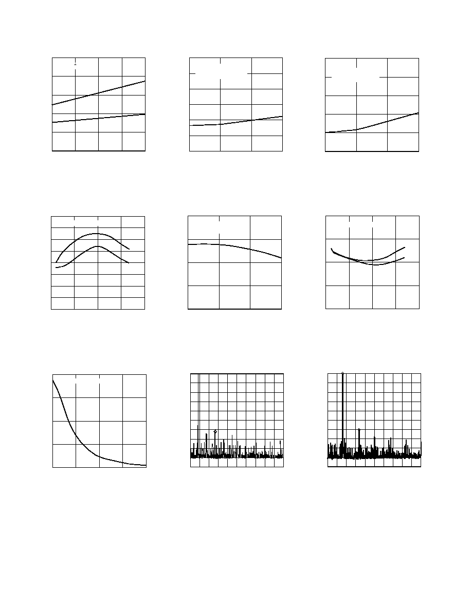
MCLK FREQUENCY MHz
TOTAL CURRENT mA
25
20
0
5
10
25
15
20
15
10
5
+5V
+3.3V
T
A
= +25 C
Figure 5. Typical Current Consump-
tion vs. MCLK Frequency
10MHz
f
OUT
/f
MCLK
SFDR (
±
2
M
Hz) dB
40
45
80
0
0.1
0.4
0.2
0.3
60
65
70
75
50
55
AVDD = DVDD = +3.3V
25MHz
Figure 8. Wide Band SFDR vs. f
OUT
/
f
MCLK
for Various MCLK Frequencies
TEMPERATURE
°
C
WAKE-UP TIME ms
10
7.5
0
40
30
0
20
10
5.0
2.5
AVDD = DVDD = +2.97V
Figure 11. Wake-Up Time vs.
Temperature
Typical Performance Characteristics
MCLK FREQUENCY MHz
SFDR (
±
50kHz) dB
50
55
80
10
0
25
20
60
65
75
70
f
OUT
/f
MCLK
= 1/3
AVDD = DVDD = +3.3V
Figure 6. Narrow Band SFDR vs.
MCLK Frequency
MCLK FREQUENCY MHz
SNR dB
60
55
40
10
15
25
20
50
45
AVDD = DVDD = +3.3V
f
OUT
= f
MCLK
/3
Figure 9. SNR vs. MCLK Frequency
VBW 1kHz
10dB/DIV
0
70
100
START 0Hz
RBW 300Hz
STOP 12.5MHz
ST 277 SEC
10
60
80
90
40
50
20
30
Figure 12. f
MCLK
= 25 MHz, f
OUT
= 1.1 MHz,
Frequency Word = B439581
MCLK FREQUENCY MHz
SFDR (
±
2
M
Hz) dB
40
45
65
10
15
25
20
50
55
60
f
OUT
/f
MCLK
= 1/3
AVDD = DVDD = +3.3V
Figure 7. Wide Band SFDR vs. MCLK
Frequency
10MHz
25MHz
f
OUT
/f
MCLK
SNR dB
60
55
40
0
0.1
0.4
0.2
0.3
50
45
AVDD = DVDD = +3.3V
Figure 10. SNR vs. f
OUT
/f
MCLK
for Vari-
ous MCLK Frequencies
VBW 1kHz
10dB/DIV
0
70
100
START 0Hz
RBW 300Hz
STOP 12.5MHz
ST 277 SEC
10
60
80
90
40
50
20
30
Figure 13. f
MCLK
= 25 MHz, f
OUT
= 2.1 MHz,
Frequency Word = 15810625
7
AD9832
REV. A
VBW 1kHz
10dB/DIV
0
70
100
START 0Hz
RBW 300Hz
STOP 12.5MHz
ST 277 SEC
10
60
80
90
40
50
20
30
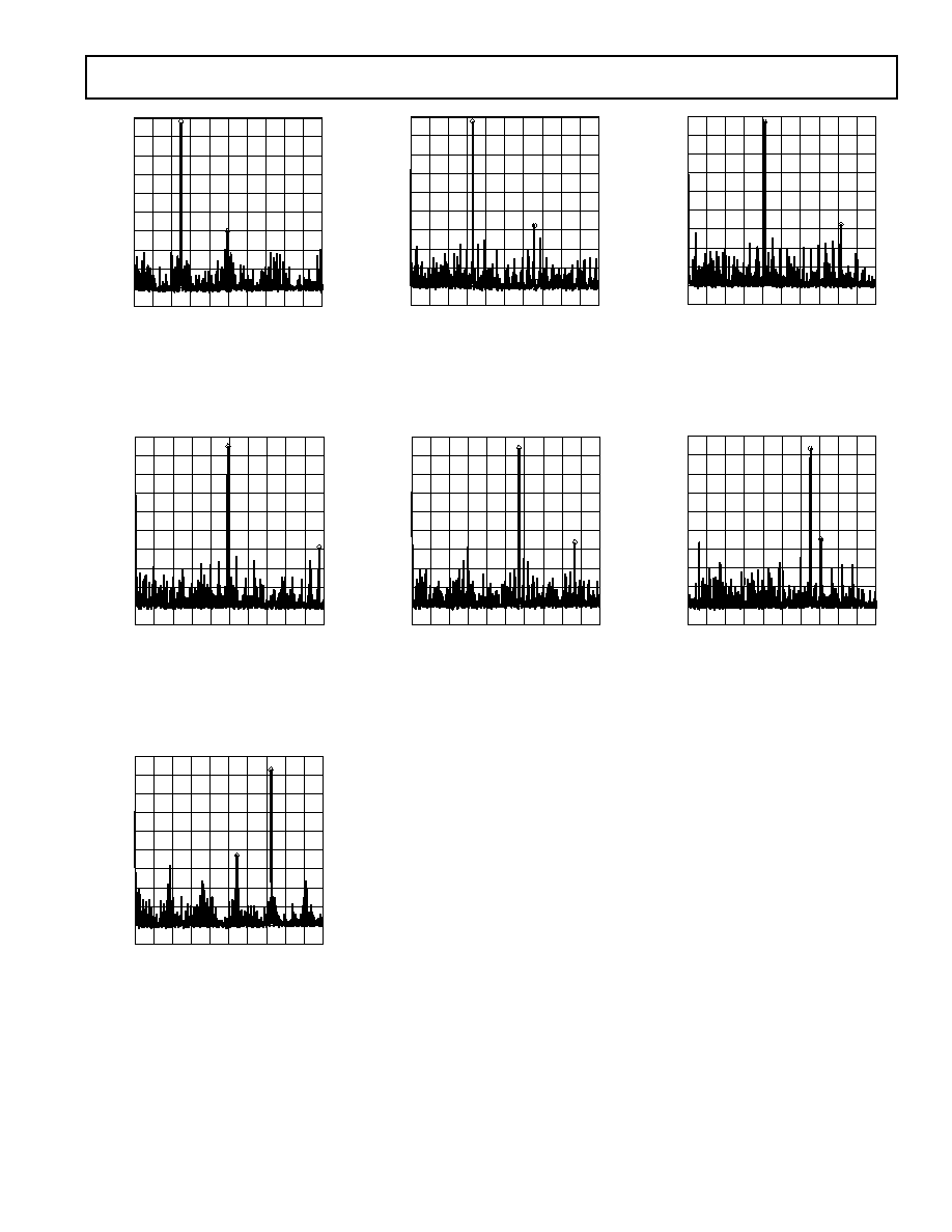
Figure 14. f
MCLK
= 25 MHz, f
OUT
= 3.1 MHz,
Frequency Word = 1FBE76C9
VBW 1kHz
10dB/DIV
0
70
100
START 0Hz
RBW 300Hz
STOP 12.5MHz
ST 277 SEC
10
60
80
90
40
50
20
30
Figure 17. f
MCLK
= 25 MHz, f
OUT
= 6.1 MHz,
Frequency Word = 3E76C8B4
VBW 1kHz
10dB/DIV
0
70
100
START 0Hz
RBW 300Hz
STOP 12.5MHz
ST 277 SEC
10
60
80
90
40
50
20
30
Figure 20. f
MCLK
= 25 MHz, f
OUT
= 9.1 MHz,
Frequency Word = 5D2F1AA0
VBW 1kHz
10dB/DIV
0
70
100
START 0Hz
RBW 300Hz
STOP 12.5MHz
ST 277 SEC
10
60
80
90
40
50
20
30
Figure 15. f
MCLK
= 25 MHz, f
OUT
= 4.1 MHz,
Frequency Word = 29FBE76D
VBW 1kHz
10dB/DIV
0
70
100
START 0Hz
RBW 300Hz
STOP 12.5MHz
ST 277 SEC
10
60
80
90
40
50
20
30
Figure 18. f
MCLK
= 25 MHz, f
OUT
= 7.1 MHz,
Frequency Word = 48B43958
VBW 1kHz
10dB/DIV
0
70
100
START 0Hz
RBW 300Hz
STOP 12.5MHz
ST 277 SEC
10
60
80
90
40
50
20
30
Figure 16. f
MCLK
= 25 MHz, f
OUT
= 5.1 MHz,
Frequency Word = 34395810
VBW 1kHz
10dB/DIV
0
70
100
START 0Hz
RBW 300Hz
STOP 12.5MHz
ST 277 SEC
10
60
80
90
40
50
20
30
Figure 19. f
MCLK
= 25 MHz, f
OUT
= 8.1 MHz,
Frequency Word = 52F1A9FC
AD9832
8
REV. A
TERMINOLOGY
Integral Nonlinearity
This is the maximum deviation of any code from a straight line
passing through the endpoints of the transfer function. The end-
points of the transfer function are zero scale, a point 0.5 LSB be-
low the first code transition (000 . . . 00 to 000 . . . 01) and full
scale, a point 0.5 LSB above the last code transition (111 . . . 10
to 111 . . . 11). The error is expressed in LSBs.
Differential Nonlinearity
This is the difference between the measured and ideal 1 LSB
change between two adjacent codes in the DAC.
Signal to (Noise + Distortion)
Signal to (Noise + Distortion) is measured signal to noise at the
output of the DAC. The signal is the rms magnitude of the
fundamental. Noise is the rms sum of all the nonfundamental
signals up to half the sampling frequency (f
MCLK
/2) but exclud-
ing the dc component. Signal to (Noise + Distortion) is depen-
dent on the number of quantization levels used in the digitization
process; the more levels, the smaller the quantization noise. The
theoretical Signal to (Noise + Distortion) ratio for a sine wave
input is given by
Signal to (Noise + Distortion) = (6.02N + 1.76) dB
where N is the number of bits. Thus, for an ideal 10-bit con-
verter, Signal to (Noise + Distortion) = 61.96 dB.
Total Harmonic Distortion
Total Harmonic Distortion (THD) is the ratio of the rms
sum of harmonics to the rms value of the fundamental. For
the AD9832, THD is defined as:
THD
=
20 log
V
2
2
+
V
3
2
+
V
4
2
+
V
5
2
+
V
6
2
V
1
where V
1
is the rms amplitude of the fundamental and V
2
, V
3
,
V
4
, V
5
and V
6
are the rms amplitudes of the second through the
sixth harmonic.
Output Compliance
The output compliance refers to the maximum voltage that can
be generated at the output of the DAC to meet the specifica-
tions. When voltages greater than those specified for the output
compliance are generated, the AD9832 may not meet the speci-
fications listed in the data sheet.
Spurious Free Dynamic Range
Along with the frequency of interest, harmonics of the fundamental
frequency and images of the MCLK frequency are present at the
output of a DDS device. The spurious free dynamic range (SFDR)
refers to the largest spur or harmonic present in the band of
interest. The wide band SFDR gives the magnitude of the larg-
est harmonic or spur relative to the magnitude of the fundamental
frequency in the bandwidth
±
2 MHz about the fundamental fre-
quency. The narrow band SFDR gives the attenuation of the
largest spur or harmonic in a bandwidth of
±
50 kHz about the
fundamental frequency.
Clock Feedthrough
There will be feedthrough from the MCLK input to the analog
output. Clock feedthrough refers to the magnitude of the MCLK
signal relative to the fundamental frequency in the AD9832's out-
put spectrum.
Table I. Control Registers
Register
Size
Description
FREQ0 REG
32 Bits
Frequency Register 0. This de-
fines the output frequency, when
FSELECT = 0, as a fraction of
the MCLK frequency.
FREQ1 REG
32 Bits
Frequency Register 1. This de-
fines the output frequency, when
FSELECT = 1, as a fraction of
the MCLK frequency.
PHASE0 REG
12 Bits
Phase Offset Register 0. When
PSEL0 = PSEL1 = 0, the contents
of this register are added to the
output of the phase accumulator.
PHASE1 REG
12 Bits
Phase Offset Register 1. When
PSEL0 = 1 and PSEL1 = 0, the
contents of this register are added to
the output of the phase accumulator.
PHASE2 REG
12 Bits
Phase Offset Register 2. When
PSEL0 = 0 and PSEL1 = 1, the con-
tents of this register are added to
the output of the phase accumulator.
PHASE3 REG
12 Bits
Phase Offset Register 3. When
PSEL0 = PSEL1 = 1, the contents
of this register are added to the
output of the phase accumulator.
Table II. Addressing the Registers
A3
A2
A1
A0
Destination Register
0
0
0
0
FREQ0 REG 8 L LSBs
0
0
0
1
FREQ0 REG 8 H LSBs
0
0
1
0
FREQ0 REG 8 L MSBs
0
0
1
1
FREQ0 REG 8 H MSBs
0
1
0
0
FREQ1 REG 8 L LSBs
0
1
0
1
FREQ1 REG 8 H LSBs
0
1
1
0
FREQ1 REG 8 L MSBs
0
1
1
1
FREQ1 REG 8 H MSBs
1
0
0
0
PHASE0 REG 8 LSBs
1
0
0
1
PHASE0 REG 8 MSBs
1
0
1
0
PHASE1 REG 8 LSBs
1
0
1
1
PHASE1 REG 8 MSBs
1
1
0
0
PHASE2 REG 8 LSBs
1
1
0
1
PHASE2 REG 8 MSBs
1
1
1
0
PHASE3 REG 8 LSBs
1
1
1
1
PHASE3 REG 8 MSBs
Table III. 32-Bit Frequency Word
s
B
S
M
6
1
s
B
S
L
6
1
s
B
S
M
H
8
s
B
S
M
L
8
s
B
S
L
H
8
s
B
S
L
L
8
Table IV. 12-Bit Frequency Word
e
h
t
f
o
s
B
S
M
4
e
h
T
(
s
B
S
M
4
)
0
=
d
e
d
a
o
L
d
r
o
W
t
i
B
-
8
s
B
S
L
8
9
AD9832
REV. A
Table V. Commands
C3
C2
C1
C0
Command
0
0
0
0
Write 16 phase bits (Present 8 Bits + 8 Bits
in Defer Register) to Selected PHASE REG.
0
0
0
1
Write 8 phase bits to Defer Register.
0
0
1
0
Write 16 frequency bits (Present 8 Bits
+ 8 Bits in Defer Register) to Selected
FREQ REG.
0
0
1
1
Write 8 frequency bits to Defer Register.
0
1
0
0
Bits D9 (PSEL0) and D10 (PSEL1) are
used to Select the PHASE REG when
SELSRC = 1. When SELSRC = 0, the
PHASE REG is Selected using the pins
PSEL0 and PSEL1.
0
1
0
1
Bit D11 is used to Select the FREQ REG
when SELSRC = 1. When SELSRC = 0,
the FREQ REG is Selected using the pin
FSELECT.
0
1
1
0
To control the PSEL0, PSEL1 and
FSELECT bits using only one write, this
command is used. Bits D9 and D10 are
used to Select the PHASE REG and Bit
11 is used to Select the FREQ REG when
SELSRC = 1. When SELSRC = 0, the
PHASE REG is Selected using the pins
PSEL0 and PSEL1 and the FREQ REG
is Selected using the pin FSELECT.
0
1
1
1
Reserved. Configures the AD9832 for
Test Purposes.
Table VI. Controlling the AD9832
D15 D14 Command
1
0
Selects source of Control for the PHASE and FREQ
Registers and Enables Synchronization.
Bit D13 is the SYNC Bit. When this bit is High,
reading of the FSELECT, PSEL0 and PSEL1 bits/
pins and the loading of the Destination Register with
data is synchronized with the rising edge of MCLK.
The latency is increased by 2 MCLK cycles when
SYNC = 1. When SYNC = 0, the loading of the
data and the sampling of FSELECT/PSEL0/PSEL1
occurs asynchronously.
Bit D12 is the Select Source Bit (SELSRC). When
this bit Equals 1, the PHASE/FREQ REG is
Selected using the bits FSELECT, PSEL0 and
PSEL1. When SELSRC = 0, the PHASE/FREQ
REG is Selected using the pins FSELECT, PSEL0
and PSEL1.
1
1
Sleep, Reset and Clear.
D13 is the SLEEP bit. When this bit equals 1, the
AD9832 is powered down, internal clocks are
disabled and the DAC's current sources and
REFOUT are turned off. When SLEEP = 0, the
AD9832 is powered up. When RESET (D12) = 1,
the phase accumulator is set to zero phase which
corresponds to an analog output of midscale. When
CLR (D11) = 1, SYNC and SELSRC are set to
zero. CLR resets to 0 automatically.
Table VII. Writing to the AD9832 Data Registers
5
1
D
4
1
D
3
1
D
2
1
D
1
1
D
0
1
D
9
D
8
D
7
D
6
D
5
D
4
D
3
D
2
D
1
D
0
D
3
C
2
C
1
C
0
C
3
A
2
A
1
A
0
A
B
S
M
B
S
L
Table VIII. Setting SYNC and SELSRC
5
1
D
4
1
D
3
1
D
2
1
D
1
1
D
0
1
D
9
D
8
D
7
D
6
D
5
D
4
D
3
D
2
D
1
D
0
D
1
0
C
N
Y
S
C
R
S
L
E
S
X
X
X
X
X
X
X
X
X
X
X
X
Table IX. Power-Down, Resetting and Clearing the AD9832
5
1
D
4
1
D
3
1
D
2
1
D
1
1
D
0
1
D
9
D
8
D
7
D
6
D
5
D
4
D
3
D
2
D
1
D
0
D
1
1
P
E
E
L
S
T
E
S
E
R
R
L
C
X
X
X
X
X
X
X
X
X
X
X
AD9832
10
REV. A
CIRCUIT DESCRIPTION
The AD9832 provides an exciting new level of integration for
the RF/Communications system designer. The AD9832 com-
bines the Numerical Controlled Oscillator (NCO), SINE Look-
Up Table, Frequency and Phase Modulators, and a Digital-to-
Analog Converter on a single integrated circuit.
The internal circuitry of the AD9832 consists of three main
sections. They are:
· Numerical Controlled Oscillator (NCO) + Phase Modulator
· SINE Look-Up Table
· Digital-to-Analog Converter
The AD9832 is a fully integrated Direct Digital Synthesis (DDS)
chip. The chip requires one reference clock, one low precision
resistor and eight decoupling capacitors to provide digitally
created sine waves up to 12.5 MHz. In addition to the genera-
tion of this RF signal, the chip is fully capable of a broad range
of simple and complex modulation schemes. These modula-
tion schemes are fully implemented in the digital domain, allow-
ing accurate and simple realization of complex modulation
algorithms using DSP techniques.
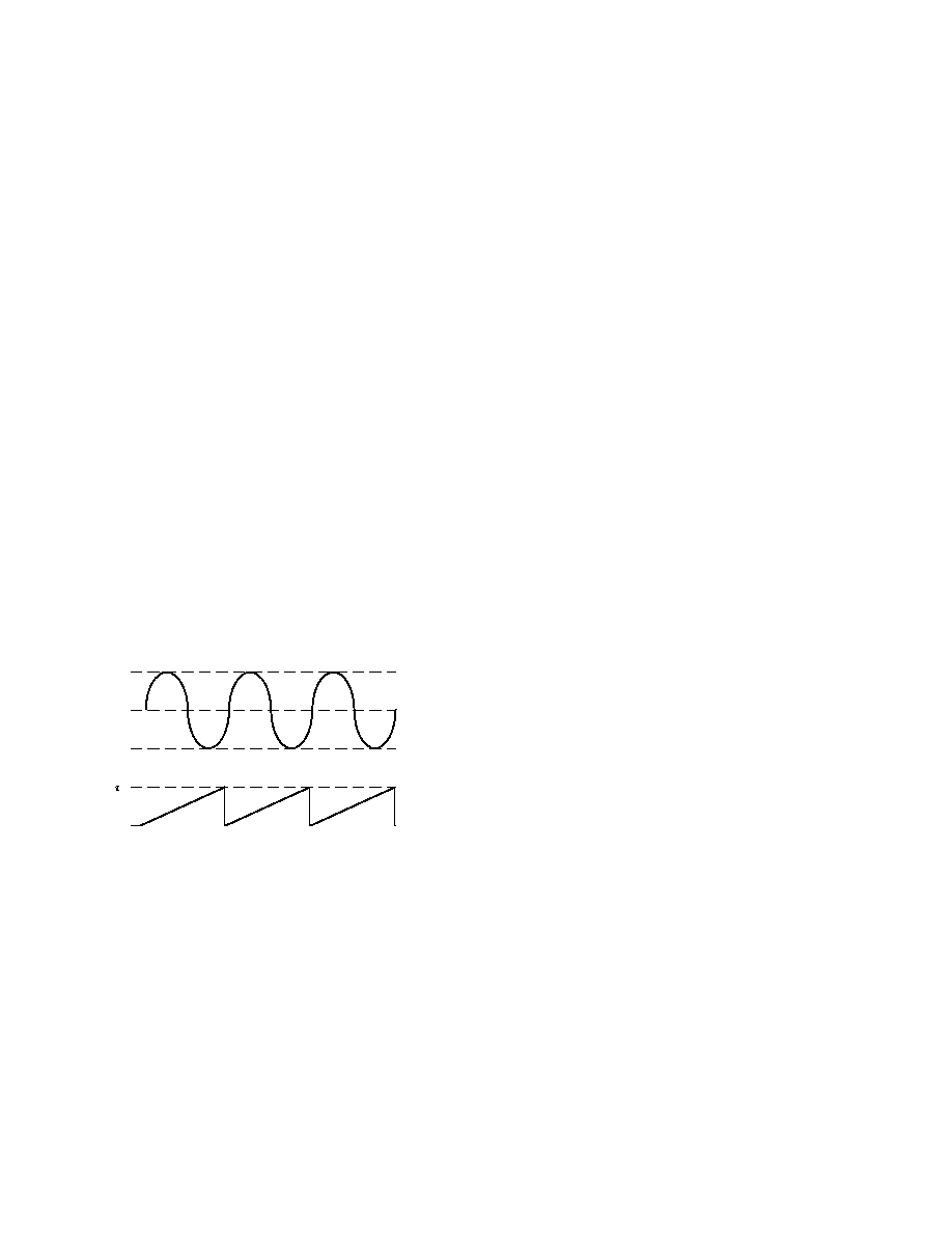
THEORY OF OPERATION
Sine waves are typically thought of in terms of their magnitude
form a(t) = sin (
t). However, these are nonlinear and not easy
to generate except through piecewise construction. On the other
hand, the angular information is linear in nature. That is, the
phase angle rotates through a fixed angle for each unit of time.
The angular rate depends on the frequency of the signal by the
traditional rate of
= 2
f.
MAGNITUDE
PHASE
+1
0
1
2
0
Figure 21. Sine Wave
Knowing that the phase of a sine wave is linear and given a
reference interval (clock period), the phase rotation for that
period can be determined.
Phase =
t
Solving for
=
Phase/
t = 2
f
Solving for f and substituting the reference clock frequency for
the reference period (1/f
MCLK
=
t)
f =
Phase
×
f
MCLK
/2
The AD9832 builds the output based on this simple equation. A
simple DDS chip can implement this equation with three major
subcircuits.
Numerical Controlled Oscillator + Phase Modulator
This consists of two frequency select registers, a phase accumu-
lator and four phase offset registers. The main component of the
NCO is a 32-bit phase accumulator that assembles the phase
component of the output signal. Continuous time signals have a
phase range of 0 to 2
. Outside this range of numbers, the
sinusoid functions repeat themselves in a periodic manner. The
digital implementation is no different. The accumulator simply
scales the range of phase numbers into a multibit digital word.
The phase accumulator in the AD9832 is implemented with 32
bits. Therefore, in the AD9832, 2
= 2
32
. Likewise, the
Phase
term is scaled into this range of numbers 0 <
Phase < 2
32
1.
Making these substitutions into the equation above
f =
Phase
×
f
MCLK
/2
32
where 0 <
Phase < 2
32
.
The input to the phase accumulator (i.e., the phase step) can be
selected from either the FREQ0 Register or FREQ1 Register
and this is controlled by the FSELECT pin or the FSELECT
bit. NCOs inherently generate continuous phase signals, thus
avoiding any output discontinuity when switching between
frequencies.
Following the NCO, a phase offset can be added to perform
phase modulation using the 12-bit PHASE Registers. The con-
tents of this register are added to the most significant bits of the
NCO. The AD9832 has four PHASE registers, the resolution of
these registers being 2
/4096.
Sine Look-Up Table (LUT)
To make the output useful, the signal must be converted from
phase information into a sinusoidal value. Since phase informa-
tion maps directly into amplitude, a ROM LUT converts the
phase information into amplitude. To do this, the digital phase
information is used to address a sine ROM LUT. Although the
NCO contains a 32-bit phase accumulator, the output of the
NCO is truncated to 12 bits. Using the full resolution of the
phase accumulator is impractical and unnecessary as this would
require a look-up table of 2
32
entries.
It is necessary only to have sufficient phase resolution in the
LUTs so the dc error of the output waveform is dominated by
the quantization error in the DAC. This requires the look-up
table to have two more bits of phase resolution than the 10-bit
DAC.
Digital-to-Analog Converter
The AD9832 includes a high impedance current source 10-bit
DAC, capable of driving a wide range of loads at different
speeds. Full-scale output current can be adjusted, for optimum
power and external load requirements, through the use of a
single external resistor (R
SET
).
The DAC is configured for single-ended operation. The load
resistor can be any value required, as long as the full-scale volt-
age developed across it does not exceed the voltage compliance
range. Since full-scale current is controlled by R
SET
, adjust-
ments to R
SET
can balance changes made to the load resistor.
However, if the DAC full-scale output current is significantly
less than 4 mA, the DAC's linearity may degrade.
DSP and MPU Interfacing
The AD9832 has a serial interface, with 16 bits being loaded
during each write cycle. SCLK, SDATA and FSYNC are used
to load the word into the AD9832. When FSYNC is taken low,
the AD9832 is informed that a word is being written to the

11
AD9832
REV. A
device. The first bit is read into the device on the next SCLK
falling edge with the remaining bits being read into the device
on the subsequent SCLK falling edges. FSYNC frames the
16 bits, therefore, when 16 SCLK falling edges have occurred,
FSYNC should be taken high again. The SCLK can be continu-
ous or, alternatively, the SCLK can idle high or low between
write operations.
When writing to a frequency/phase register, the first four bits
identify whether a frequency or phase register is being written
to, the next four bits contain the address of the destination
register while the 8 LSBs contain the data. Table II lists the
addresses for the phase/frequency registers while Table III lists
the commands.
Within the AD9832, 16-bit transfers are used when loading the
destination frequency/phase register. There are two modes for
loading a register--direct data transfer and a deferred data
transfer. With a deferred data transfer, the 8-bit word is loaded
into the defer register (8 LSBs or 8 MSBs). However, this data
is not loaded into the 16-bit data register so the destination
register is not updated. With a direct data transfer, the 8-bit
word is loaded into the appropriate defer register (8 LSBs or
8 MSBs). Immediately following the loading of the defer regis-
ter, the contents of the complete defer register are loaded into
the 16-bit data register and the destination register is loaded on
the next MCLK rising edge. When a destination register is
addressed, a deferred transfer is needed first followed by a direct
transfer. When all 16 bits of the defer register contain relevant
data, the destination register can then be updated using 8-bit
loading rather than 16-bit loading i.e., direct data transfers can
be used. For example, after a new 16-bit word has been loaded
to a destination register, the defer register will contain this word
also. If the next write instruction is to the same destination
register, the user can use direct data transfers immediately.
When writing to a phase register, the 4 MSBs of the 16-bit word
loaded into the data register should be zero (the phase registers
are 12 bits wide).
To alter the entire contents of a frequency register, four write
operations are needed. However, the 16 MSBs of a frequency
word are contained in a separate register to the 16 LSBs. There-
fore, the 16 MSBs of the frequency word can be altered inde-
pendent of the 16 LSBs.
The phase and frequency registers to be used are selected using
the pins FSELECT, PSEL0 and PSEL1 or the corresponding
bits can be used. Bit SELSRC determines whether the bits or
the pins are used. When SELSRC = 0, the pins are used while
the bits are used when SELSRC = 1. When CLR is taken high,
SELSRC is set to 0 so that the pins are the default source.
Data transfers from the serial (defer) register to the 16-bit data
register, and the FSELECT and PSEL registers, occur following
the 16th falling SCLK edge. Transfer of the data from the
16-bit data register to the destination register or from the
FSELECT/PSEL register to the respective multiplexer occurs
on the next MCLK rising edge. Since the SCLK and the
MCLK are asynchronous, an MCLK rising edge may occur
while the data bits are in transitional state, which will cause a
brief spurious DAC output if the register being written to is
generating the DAC output. To avoid such spurious outputs,
the AD9832 contains synchronizing circuitry. When the SYNC
bit is set to 1, the synchronizer is enabled and data transfers
from the serial register (defer register) to the 16-bit data register
and the FSELECT/PSEL registers occur following a two stage
pipeline delay which is triggered on the MCLK falling edge.
The pipeline delay ensures that the data is valid when the trans-
fer occurs. Similarly, selection of the frequency/phase registers
using the FSELECT/PSEL pins is synchronized with the
MCLK rising edge when SYNC = 1. When SYNC = 0, the
synchronizer is bypassed.
Selecting the frequency/phase registers using the pins is synchro-
nized with MCLK internally also when SYNC = 1 to ensure
that these inputs are valid at the MCLK rising edge. If times t
11
and t
11A
are met, then the inputs will be at steady state at the
MCLK rising edge. However, if times t
11
and t
11A
are violated,
the internal synchronizing circuitry will delay the instant at
which the pins are sampled, ensuring that the inputs are valid at
the sampling instant.
Associated with each operation is a latency. When inputs
FSELECT/PSEL change value, there will be a pipeline delay
before control is transferred to the selected register--there will
be a pipeline delay before the analog output is controlled by the
selected register. When times t
11
and t
11A
are met, PSEL0,
PSEL1 and FSELECT have latencies of six MCLK cycles when
SYNC = 0. When SYNC = 1, the latency is increased to 8 MCLK
cycles. When times t
11
and t
11A
are not met, the latency can
increase by one MCLK cycle. Similarly, there is a latency asso-
ciated with each write operation. If a selected frequency/phase
register is loaded with a new word, there is a delay of 6 to 7
MCLK cycles before the analog output will change (there is an
uncertainty of one MCLK cycle regarding the MCLK rising
edge at which the data is loaded into the destination register).
When SYNC = 1, the latency will be 8 or 9 MCLK cycles.
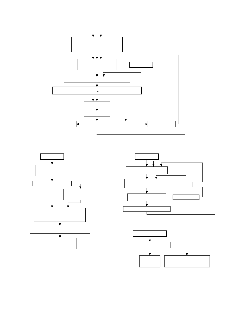
The flow chart in Figure 22 shows the operating routine for the
AD9832. When the AD9832 is powered up, the part should be
reset. This will reset the phase accumulator to zero so that the
analog output is at midscale. To avoid spurious DAC outputs
while the AD9832 is being initialized, the RESET bit should be
set to 1 until the part is ready to begin generating an output.
Taking CLR high will set SYNC and SELSRC to 0 so that
the FSELECT/PSEL pins are used to select the frequency/
phase registers and the synchronization circuitry is bypassed.
A write operation is needed to the SYNC/SELSRC register to
enable the synchronization circuitry or to change control to
the FSELECT/PSEL bits. RESET does not reset the phase
and frequency registers. These registers will contain invalid
data and, therefore, should be set to a known value by the user.
The RESET bit is then set to 0 to begin generating an output. A
signal will appear at the DAC output 6 MCLK cycles after
RESET is set to 0.
The analog output is f
MCLK
/2
32
×
FREG where FREG is the
value loaded into the selected frequency register. This signal will
be phase shifted by the amount specified in the selected phase
register (2
/4096
×
PHASEREG where PHASEREG is the
value contained in the selected phase register).
Control of the frequency/phase registers can be interchanged
from the pins to the bits.
AD9832
12
REV. A
DATA WRITE**
FREG<0> = f
OUT0
/f
MCLK
*2
32
FREG<1> = f
OUT1
/f
MCLK
*2
32
PHASEREG <3:0> = DELTA PHASE<0, 1, 2, 3>
SELECT DATA SOURCES***
SET FSELECT
SET PSEL0, PSEL1
INITIALIZATION*
WAIT 6 MCLK CYCLES (8 MCLK CYCLES IF SYNC = 1)
DAC OUTPUT
V
OUT
= V
REFIN
*6.25*R
OUT
/R
SET
*(1 + SIN(2 (FREG*f
MCLK
*t/2
32
+ PHASEREG/2
12
)))
CHANGE PHASE?
NO
CHANGE f
OUT
?
YES
NO
YES
CHANGE f
OUT
?
NO
YES
CHANGE FSELECT
CHANGE PHASEREG?
NO
YES
CHANGE PSEL0, PSEL1
Figure 22. Flow Chart for AD9832 Initialization and Operation
INITIALIZATION*
CONTROL REGISTER WRITE
SET SLEEP
RESET = 1
CLR = 1
SET SYNC AND/OR SELSRC TO 1
YES
NO
CONTROL REGISTER WRITE
SYNC = 1
AND/OR
SELSRC = 1
WRITE INITIAL DATA
FREG<0> = f
OUT0
/f
MCLK
*2
32
FREG<1> = f
OUT1
/f
MCLK
*2
32
PHASEREG<3:0> = DELTA PHASE<0, 1, 2, 3>
SET PINS OR FREQUENCY/PHASE REGISTER WRITE
SET FSELECT, PSEL0 AND PSEL1
CONTROL REGISTER WRITE
SLEEP = 0
RESET = 0
CLR = 0
Figure 23. Initialization
DATA WRITE**
DEFERRED TRANSFER WRITE
WRITE 8 BITS TO DEFER REGISTER
DIRECT TRANSFER WRITE
WRITE PRESENT 8 BITS AND 8 BITS IN
DEFER REGISTER TO DATA REGISTER
WRITE ANOTHER WORD TO THIS
REGISTER?
WRITE A WORD TO ANOTHER REGISTER
CHANGE 8 BITS ONLY
YES
NO
CHANGE 16 BITS
NO
YES
Figure 24. Data Writes
SELECT DATA SOURCES***
FSELECT/PSEL PINS BEING USED?
YES
SELSRC = 0
SET PINS
SET FSELECT
SET PSEL0
SET PSEL1
FREQUENCY/PHASE REGISTER WRITE
SET FSELECT
SET PSEL0
SET PSEL1
NO
SELSRC = 1
Figure 25. Selecting Data Sources
13
AD9832
REV. A
APPLICATIONS
The AD9832 contains functions that make it suitable for modu-
lation applications. The part can be used to perform simple
modulation such as FSK, and more complex modulation
schemes such as GMSK and QPSK can also be implemented
using the AD9832. In an FSK application, the two frequency
registers of the AD9832 are loaded with different values; one
frequency will represent the space frequency while the other will
represent the mark frequency. The digital data stream is fed to
the FSELECT pin, which will cause the AD9832 to modulate
the carrier frequency between the two values.
The AD9832 has four phase registers; this enables the part to
perform PSK. With phase shift keying, the carrier frequency is
phase shifted, the phase being altered by an amount which is
related to the bit stream being input to the modulator. The
presence of four shift registers eases the interaction needed
between the DSP and the AD9832.
The AD9832 is also suitable for signal generator applications.
With its low current consumption, the part is suitable for appli-
cations in which it can be used as a local oscillator. In addition,
the part is fully specified for operation with a +3.3 V
±
10%
power supply. Therefore, in portable applications where current
consumption is an important issue, the AD9832 is perfect.
Grounding and Layout
The printed circuit board that houses the AD9832 should be
designed so the analog and digital sections are separated and
confined to certain areas of the board. This facilitates the use of
ground planes that can be easily separated. A minimum etch
technique is generally best for ground planes as it gives the best
shielding. Digital and analog ground planes should only be
joined in one place. If the AD9832 is the only device requiring
an AGND to DGND connection, the ground planes should
be connected at the AGND and DGND pins of the AD9832.
If the AD9832 is in a system where multiple devices require
AGND to DGND connections, the connection should be made
at one point only, a star ground point that should be established
as close as possible to the AD9832.
Avoid running digital lines under the device as these will couple
noise onto the die. The analog ground plane should be allowed
to run under the AD9832 to avoid noise coupling. The power
supply lines to the AD9832 should use as large a track as pos-
sible to provide low impedance paths and reduce the effects of
glitches on the power supply line. Fast switching signals such as
clocks should be shielded with digital ground to avoid radiating
noise to other sections of the board. Avoid crossover of digital
and analog signals. Traces on opposite sides of the board should
run at right angles to each other. This will reduce the effects of
feedthrough through the board. A microstrip technique is by far
the best but is not always possible with a double-sided board. In
this technique, the component side of the board is dedicated to
ground planes while signals are placed on the other side.
Good decoupling is important. The analog and digital supplies
to the AD9832 are independent and separately pinned out to
minimize coupling between analog and digital sections of the
device. All analog and digital supplies should be decoupled to
AGND and DGND respectively with 0.1
µ
F ceramic capacitors
in parallel with 10
µ
F tantalum capacitors. To achieve the best
from the decoupling capacitors, they should be placed as close
as possible to the device, ideally right up against the device. In
systems where a common supply is used to drive both the
AVDD and DVDD of the AD9832, it is recommended that the
system's AVDD supply be used. This supply should have the
recommended analog supply decoupling between the AVDD
pins of the AD9832 and AGND and the recommended digital
supply decoupling capacitors between the DVDD pins and
DGND.
Interfacing the AD9832 to Microprocessors
The AD9832 has a standard serial interface that allows the part
to interface directly with several microprocessors. The device
uses an external serial clock to write the data/control information
into the device. The serial clock can have a frequency of 20 MHz
maximum. The serial clock can be continuous, or it can idle
high or low between write operations. When data/control infor-
mation is being written to the AD9832, FSYNC is taken low
and held low while the 16 bits of data are being written into the
AD9832. The FSYNC signal frames the 16 bits of information
being loaded into the AD9832.
AD9832 to ADSP-21xx Interface
Figure 26 shows the serial interface between the AD9832 and
the ADSP-21xx. The ADSP-21xx should be set up to operate in
the SPORT Transmit Alternate Framing Mode (TFSW = 1).
The ADSP-21xx is programmed through the SPORT control
register and should be configured as follows: internal clock
operation (ISCLK = 1), active low framing (INVTFS = 1),
16-bit word length (SLEN = 15), internal frame sync signal
(ITFS = 1), generate a frame sync for each write operation
(TFSR = 1). Transmission is initiated by writing a word to the
Tx register after the SPORT has been enabled. The data is
clocked out on each rising edge of the serial clock and clocked
into the AD9832 on the SCLK falling edge.
ADSP-2101/
ADSP-2103
AD9832
TFS
DT
SCLK
FSYNC
ADDITIONAL PINS OMITTED FOR CLARITY
SDATA
SCLK
Figure 26. ADSP-2101/ADSP-2103 to AD9832 Interface
AD9832
14
REV. A
AD9832 to 68HC11/68L11 Interface
Figure 27 shows the serial interface between the AD9832 and
the 68HC11/68L11 microcontroller. The microcontroller is
configured as the master by setting bit MSTR in the SPCR to 1
and this provides a serial clock on SCK while the MOSI output
drives the serial data line SDATA. Since the microcontroller
does not have a dedicated frame sync pin, the FSYNC signal is
derived from a port line (PC7). The set-up conditions for cor-
rect operation of the interface are as follows: the SCK idles high
between write operations (CPOL = 0), data is valid on the SCK
falling edge (CPHA = 1). When data is being transmitted to the
AD9832, the FSYNC line is taken low (PC7). Serial data
from the 68HC11/68L11 is transmitted in 8-bit bytes with
only 8 falling clock edges occurring in the transmit cycle. Data
is transmitted MSB first. In order to load data into the AD9832,
PC7 is held low after the first 8 bits are transferred and a second
serial write operation is performed to the AD9832. Only after
the second 8 bits have been transferred should FSYNC be taken
high again.
68HC11/68L11
AD9832
PC7
MOSI
SCK
SDATA
SCLK
FSYNC
ADDITIONAL PINS OMITTED FOR CLARITY
Figure 27. 68HC11/68L11 to AD9832 Interface
AD9832 to 80C51/80L51 Interface
Figure 28 shows the serial interface between the AD9832 and
the 80C51/80L51 microcontroller. The microcontroller is oper-
ated in Mode 0 so that TXD of the 80C51/80L51 drives SCLK
of the AD9832 while RXD drives the serial data line SDATA.
The FSYNC signal is again derived from a bit programmable
pin on the port (P3.3 being used in the diagram). When data is
to be transmitted to the AD9832, P3.3 is taken low. The
80C51/80L51 transmits data in 8-bit bytes thus, only 8 falling
SCLK edges occur in each cycle. To load the remaining 8 bits
to the AD9832, P3.3 is held low after the first 8 bits have been
transmitted and a second write operation is initiated to transmit
the second byte of data. P3.3 is taken high following the comple-
tion of the second write operation. SCLK should idle high
between the two write operations. The 80C51/80L51 outputs
the serial data in a format which has the LSB first. The AD9832
accepts the MSB first (the 4 MSBs being the control informa-
tion, the next 4 bits being the address while the 8 LSBs contain
the data when writing to a destination register). Therefore, the
transmit routine of the 80C51/80L51 must take this into ac-
count and rearrange the bits so that the MSB is output first.
80C51/80L51
AD9832
P3.3
RXD
TXD
SDATA
SCLK
FSYNC
ADDITIONAL PINS OMITTED FOR CLARITY
Figure 28. 80C51/80L51 to AD9832 Interface
AD9832 to DSP56002 Interface
Figure 29 shows the interface between the AD9832 and the
DSP56002. The DSP56002 is configured for normal mode
asynchronous operation with a gated internal clock (SYN = 0,
GCK = 1, SCKD = 1). The frame sync pin is generated inter-
nally (SC2 = 1), the transfers are 16-bits wide (WL1 = 1, WL0
= 0) and the frame sync signal will frame the 16 bits (FSL = 0).
The frame sync signal is available on Pin SC2, but it needs to be
inverted before being applied to the AD9832. The interface to
the DSP56000/DSP56001 is similar to that of the DSP56002.
DSP56002
AD9832
SC2
STD
SCK
SDATA
SCLK
FSYNC
ADDITIONAL PINS OMITTED FOR CLARITY
Figure 29. AD9832 to DSP56002 Interface
AD9832 Evaluation Board
The AD9832 Evaluation Board allows designers to evaluate the
high performance AD9832 DDS modulator with a minimum of
effort.
To prove that this device will meet the user's waveform synthe-
sis requirements, the user requires only a 3.3 V or 5 V power
supply, an IBM-compatible PC and a spectrum analyzer along
with the evaluation board. The evaluation board setup is shown
below.
The DDS evaluation kit includes a populated, tested AD9832
printed circuit board, along with the software that controls the
AD9832, in a Windows environment.
AD9832.EXE
IBM-COMPATIBLE PC
PARALLEL PORT
CENTRONICS
PRINTER CABLE
AD9832 EVALUATION
BOARD
Figure 30. AD9832 Evaluation Board Setup
15
AD9832
REV. A
Using the AD9832 Evaluation Board
The AD9832 Evaluation kit is a test system designed to simplify
the evaluation of the AD9832. Provisions to control the AD9832
from the printer port of an IBM-compatible PC are included,
along with the necessary software. An application note is also
available with the evaluation board and gives information on
operating the evaluation board.
Prototyping Area
An area is available on the evaluation board for the user to add
additional circuits to the evaluation test set. Users may want to
build custom analog filters for the output or add buffers and
operational amplifiers to be used in the final application.
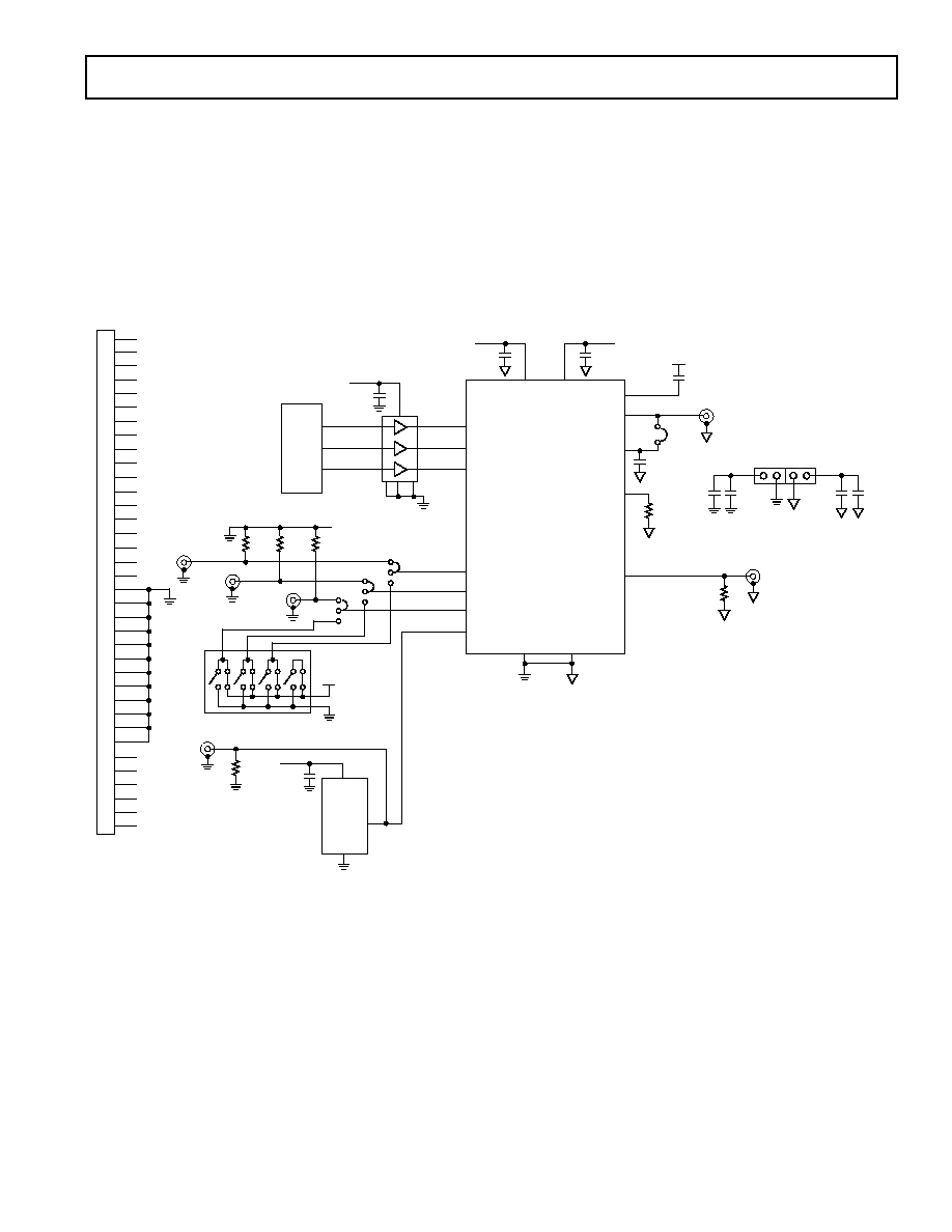
C1
0.1 F
DVDD
AVDD
C2
0.1 F
4
15
DVDD
AVDD
16
2
3
1
14
COMP
REFIN
REFOUT
FSADJUST
IOUT
AVDD
C3
10nF
REFIN
C4
10nF
LK4
R5
3.9k
IOUT
C8
10 F
C7
0.1 F
DVDD
J2
J3
C9
0.1 F
C10
10 F
AVDD
R6
300
DGND
AGND
5
13
11
12
10
6
9
8
7
MCLK
FSELECT
PSEL0
PSEL1
FSYNC
SDATA
SCLK
16
14
9
20
11
6
4
DVDD
C6
0.1 F
1 10 19
U2
J1
SCLK
SDATA
FSYNC
R3
10k
R1
10k
R2
10k
PSEL1
PSEL0
FSELECT
LK1
LK2
LK3
SW
DVDD
MCLK
R4
50
DGND
DVDD
OUT
DVDD
C5
0.1 F
U3
SCLK
SDATA
FSYNC
1
2
3
4
5
6
7
8
9
10
11
12
13
14
15
16
17
18
19
20
21
22
23
24
25
26
27
28
29
30
31
32
33
34
35
36
U1
AD9832
XTAL1
Figure 31. AD9832 Evaluation Board Layout
XO vs. External Clock
The AD9832 can operate with master clocks up to 25 MHz. A
25 MHz oscillator is included on the evaluation board. How-
ever, this oscillator can be removed and, if required, an external
CMOS clock connected to the part.
Power Supply
Power to the AD9832 Evaluation Board must be provided ex-
ternally through the pin connections. The power leads should be
twisted to reduce ground loops.
Integrated Circuits
XTAL1
OSC XTAL 25 MHz
U1
AD9832 (16-Pin TSSOP)
U2
74HCT244 Buffer
Capacitors
C1, C2
0.1
µ
F Ceramic Chip Capacitor
C3, C4
10 nF Ceramic Capacitor
C5, C6, C7, C9
0.1
µ
F Ceramic Capacitor
C8, C10
10
µ
F Tantalum Capacitor
Resistors
R1R3
10 k
Resistor
R4
50
Resistor
R5
3.9 k
Resistor
R6
300
Resistor
Links
LK1LK3
Three-Pin Link
LK4
Two-Pin Link
Switch
SW
End Stackable Switch (SDC Double
Throw)
Sockets
MCLK, PSEL0,
Subminiature BNC Connector
PSEL1, FSELECT,
IOUT, REFIN
Connectors
J1
36-Pin Edge Connector
J2, J3
PCB Mounting Terminal Block
16
C3122a07/99
PRINTED IN U.S.A.
AD9832
REV. A
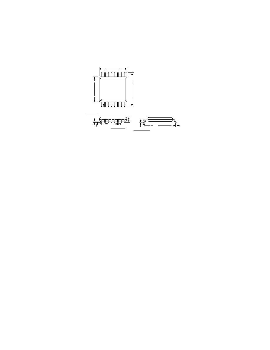
16-Lead Thin Shrink Small Outline Package (TSSOP)
(RU-16)
16
9
8
1
0.201 (5.10)
0.193 (4.90)
0.256 (6.50)
0.246 (6.25)
0.177 (4.50)
0.169 (4.30)
PIN 1
SEATING
PLANE
0.006 (0.15)
0.002 (0.05)
0.0118 (0.30)
0.0075 (0.19)
0.0256
(0.65)
BSC
0.0433
(1.10)
MAX
0.0079 (0.20)
0.0035 (0.090)
0.028 (0.70)
0.020 (0.50)
8
°
0
°
OUTLINE DIMENSIONS
Dimensions shown in inches and (mm).