AD9514 1.6 GHz Clock Distribution IC, Dividers, Delay Adjust, Three Outputs Data Sheet (Rev. 0)
1.6 GHz Clock Distribution IC,
Dividers, Delay Adjust, Three Outputs
AD9514
Rev. 0
Information furnished by Analog Devices is believed to be accurate and reliable. However, no
responsibility is assumed by Analog Devices for its use, nor for any infringements of patents or other
rights of third parties that may result from its use. Specifications subject to change without notice. No
license is granted by implication or otherwise under any patent or patent rights of Analog Devices.
Trademarks and registered trademarks are the property of their respective owners.
One Technology Way, P.O. Box 9106, Norwood, MA 02062-9106, U.S.A.
Tel: 781.329.4700
www.analog.com
Fax: 781.461.3113
© 2005 Analog Devices, Inc. All rights reserved.
FEATURES
1.6 GHz differential clock input
3 programmable dividers
Divide-by in range from1 to 32
Phase select for coarse delay adjust
2 independent 1.6 GHz LVPECL clock outputs
Additive broadband output jitter 225 fs rms
1 independent 800 MHz/250 MHz LVDS/CMOS clock output
Additive broadband output jitter 300 fs rms/290 fs rms
Time delays up to 10 ns
Device configured with 4-level logic pins
Space-saving, 32-lead LFCSP
APPLICATIONS
Low jitter, low phase noise clock distribution
Clocking high speed ADCs, DACs, DDSs, DDCs, DUCs, MxFEs
High performance wireless transceivers
High performance instrumentation
Broadband infrastructure
ATE
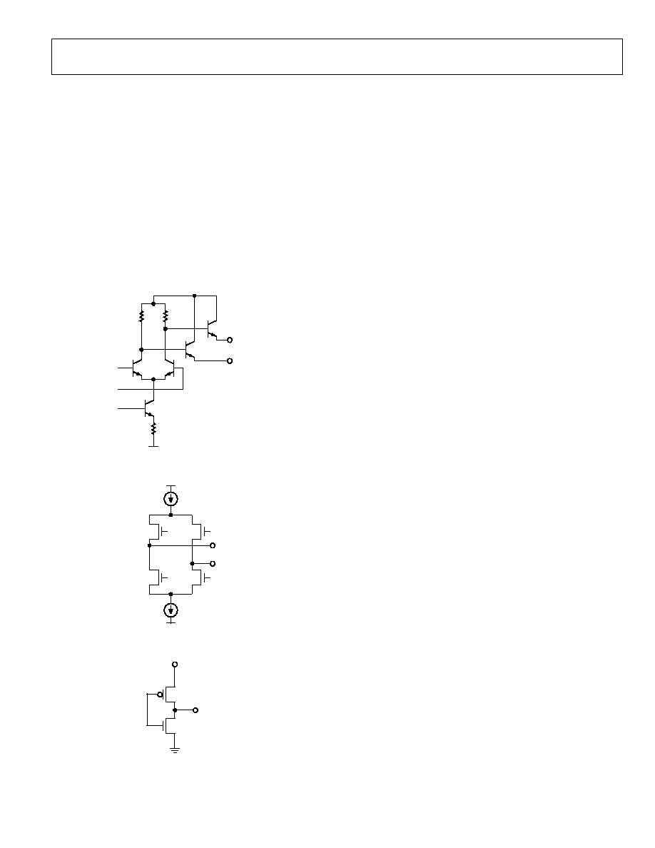
FUNCTIONAL BLOCK DIAGRAM
VREF
S10 S9
S8
S7
S6
S5
S4
S3
S2
S1
S0
SETUP LOGIC
OUT0
CLK
CLKB
SYNCB
RSET
VS
GND
OUT0B
OUT1
OUT1B
OUT2
OUT2B
AD9514
/1. . . /32
/1. . . /32
/1. . . /32
t
LVPECL
LVPECL
LVDS/CMOS
05596-
001
Figure 1.
GENERAL DESCRIPTION
The AD9514 features a multi-output clock distribution IC in a
design that emphasizes low jitter and phase noise to maximize
data converter performance. Other applications with demanding
phase noise and jitter requirements also benefit from this part.
There are three independent clock outputs. Two of the outputs
are LVPECL, and the third output can be set to either LVDS or
CMOS levels. The LVPECL outputs operate to 1.6 GHz, and the
third output operates to 800 MHz in LVDS mode and to
250 MHz in CMOS mode.
Each output has a programmable divider that can be set to
divide by a selected set of integers ranging from 1 to 32. The
phase of one clock output relative to another clock output can
be set by means of a divider phase select function that serves as
a coarse timing adjustment.
The LVDS/CMOS output features a delay element with three
selectable full-scale delay values (1.5 ns, 5 ns, and 10 ns), each
with 16 steps of fine adjustment.
The AD9514 does not require an external controller for
operation or setup. The device is programmed by means of
11 pins (S0 to S10) using 4-level logic. The programming pins
are internally biased to V
S
. The VREF pin provides a level of
V
S
. V
S
(3.3 V) and GND (0 V) provide the other two logic levels.
The AD9514 is ideally suited for data converter clocking
applications where maximum converter performance is
achieved by encode signals with subpicosecond jitter.
The AD9514 is available in a 32-lead LFCSP and operates from
a single 3.3 V supply. The temperature range is -40°C to +85°C.

AD9514
Rev. 0 | Page 2 of 28
TABLE OF CONTENTS
Features .............................................................................................. 1
Applications....................................................................................... 1
Functional Block Diagram .............................................................. 1
General Description ......................................................................... 1
Revision History ............................................................................... 2
Specifications..................................................................................... 3
Clock Input.................................................................................... 3
Clock Outputs ............................................................................... 3
Timing Characteristics ................................................................ 4
Clock Output Phase Noise .......................................................... 5
Clock Output Additive Time Jitter............................................. 8
SYNCB, VREF, and Setup Pins ................................................. 10
Power............................................................................................ 10
Timing Diagrams............................................................................ 11
Absolute Maximum Ratings.......................................................... 12
Thermal Characteristics ............................................................ 12
ESD Caution................................................................................ 12
Pin Configuration and Function Descriptions........................... 13
Terminology .................................................................................... 14
Typical Performance Characteristics ........................................... 15
Functional Description .................................................................. 18
Overall.......................................................................................... 18
CLK, CLKB--Differential Clock Input ................................... 18
Synchronization.......................................................................... 18
Power-On SYNC .................................................................... 18
SYNCB..................................................................................... 18
R
SET
Resistor ................................................................................ 19
VREF............................................................................................ 19
Setup Configuration................................................................... 19
Divider Phase Offset .................................................................. 22
Delay Block ................................................................................. 22
Outputs ........................................................................................ 23
Power Supply............................................................................... 23
Exposed Metal Paddle ........................................................... 24
Power Management ................................................................... 24
Applications..................................................................................... 25
Using the AD9514 Outputs for ADC Clock Applications.... 25
LVPECL Clock Distribution ..................................................... 25
LVDS Clock Distribution .......................................................... 26
CMOS Clock Distribution ........................................................ 26
Setup Pins (S0 to S10)................................................................ 26
Power and Grounding Considerations and Power Supply
Rejection...................................................................................... 26
Phase Noise and Jitter Measurement Setups........................... 27
Outline Dimensions ....................................................................... 28
Ordering Guide .......................................................................... 28
REVISION HISTORY
7/05--Revision 0: Initial Version
AD9514
Rev. 0 | Page 3 of 28
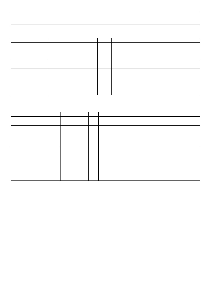
SPECIFICATIONS
Typical (typ) is given for V
S
= 3.3 V ± 5%, T
A
= 25°C, R
SET
= 4.12 k, LVPECL V
OD
= 790 mV, unless otherwise noted. Minimum (min)
and maximum (max) values are given over full V
S
and T
A
(-40°C to +85°C) variation.
CLOCK INPUT
Table 1.
Parameter
Min
Typ
Max
Unit
Test Conditions/Comments
CLOCK INPUT (CLK)
Input Frequency
1
0 1.6
GHz
Input Sensitivity
1
150
mV
p-p
Input Common-Mode Voltage, V
CM
1.5
1.6
1.7
V
Self-biased; enables ac coupling
Input Common-Mode Range, V
CMR
1.3
1.8
V
With 200 mV p-p signal applied; dc-coupled
Input Sensitivity, Single-Ended
150
mV p-p
CLK ac-coupled; CLKB ac-bypassed to RF ground
Input Resistance
4.0
4.8
5.6
k
Self-biased
Input Capacitance
2
pF
1
A slew rate of 1 V/ns is required to meet jitter, phase noise, and propagation delay specifications.
CLOCK OUTPUTS
Table 2.
Parameter
Min
Typ
Max
Unit
Test Conditions/Comments
LVPECL CLOCK OUTPUTS
Termination = 50 to V
S
- 2 V
(OUT0, OUT1) Differential
Output Frequency
0
1.6
GHz
Output High Voltage (V
OH
) V
S
- 1.1
V
S
- 0.96
V
S
- 0.82
V
Output Low Voltage (V
OL
) V
S
- 1.90
V
S
- 1.76
V
S
- 1.52
V
Output Differential Voltage (V
OD
)
640
790
960
mV
LVDS CLOCK OUTPUT
Termination = 100 differential
(OUT2) Differential
Output Frequency
0
800
MHz
Differential Output Voltage (V
OD
)
250
350
450
mV
Delta V
OD
30
mV
Output Offset Voltage (V
OS
) 1.125
1.23
1.375
V
Delta V
OS
25
mV
Short-Circuit Current (I
SA
, I
SB
)
14
24
mA
Output shorted to GND
CMOS CLOCK OUTPUT
Single-ended measurements; termination open
(OUT2) Single-Ended
Complementary output on (OUT2B)
Output Frequency
0
250
MHz
With 5 pF load
Output Voltage High (V
OH
) V
S
- 0.1
V
@ 1 mA load
Output Voltage Low (V
OL
)
0.1
V
@ 1 mA load
AD9514
Rev. 0 | Page 4 of 28
TIMING CHARACTERISTICS
CLK input slew rate = 1 V/ns or greater.
Table 3.
Parameter
Min
Typ
Max
Unit
Test Conditions/Comments
LVPECL
Termination = 50 to V
S
- 2 V
Output Rise Time, t
RP
60
100
ps
20% to 80%, measured differentially
Output Fall Time, t
FP
60
100
ps
80% to 20%, measured differentially
PROPAGATION DELAY, t
PECL
, CLK-TO-LVPECL OUT
Divide = 1
355
480
635
ps
Divide = 2 - 32
395
530
710
ps
Variation with Temperature
0.5
ps/°C
OUTPUT SKEW, LVPECL
OUT0 to OUT1 on Same Part, t
SKP
1
-50 0
+55 ps
Both LVPECL Outputs Across Multiple Parts, t
SKP_AB
2
125
ps
Same LVPECL Output Across Multiple Parts, t
SKP_AB
2
125
ps
LVDS
Termination = 100 differential, 3.5 mA
Output Rise Time, t
RL
200
350
ps
20% to 80%, measured differentially
Output Fall Time, t
FL
210
350
ps
80% to 20%, measured differentially
PROPAGATION DELAY, t
LVDS
, CLK-TO-LVDS OUT
Optional delay off
Divide = 1
1.00
1.25
1.55
ns
Divide = 2 - 32
1.05
1.30
1.60
ns
Variation with Temperature
0.9
ps/°C
OUTPUT SKEW, LVDS
Optional delay off
LVDS Output Across Multiple Parts, t
SKV_AB
2
230
ps
CMOS
B outputs are inverted; termination = open
Output Rise Time, t
RC
650
865
ps
20% to 80%; C
LOAD
= 3 pF single-ended
Output Fall Time, t
FC
650
990
ps
80% to 20%; C
LOAD
= 3 pF single-ended
PROPAGATION DELAY, t
CMOS
, CLK-TO-CMOS OUT
Optional delay off
Divide = 1
1.10
1.45
1.75
ns
Divide = 2 - 32
1.15
1.50
1.80
ns
Variation with Temperature
1
ps/°C
OUTPUT SKEW, CMOS
Optional delay off
CMOS Output Across Multiple Parts, t
SKC_AB
2
300
ps
LVPECL-TO-LVDS OUT
Output Delay, t
SKV_C
560 790 950 ps
LVPECL-TO-CMOS OUT
Output Delay, t
SKV_C
700 970 1150 ps
DELAY ADJUST (OUT2; LVDS and CMOS)
S0 = 1/3
Zero Scale Delay Time
3
0.34
ns
Zero Scale Variation with Temperature
0.20
ps/°C
Full Scale Time Delay
3
1.7
ns
Full Scale Variation with Temperature
-0.38
ps/°C
S0 = 2/3
Zero Scale Delay Time
3
0.45
ns
Zero Scale Variation with Temperature
0.31
ps/°C
Full Scale Time Delay
3
5.9
ns
Full Scale Variation with Temperature
-1.3
ps/°C
AD9514
Rev. 0 | Page 5 of 28
Parameter
Min
Typ
Max
Unit
Test Conditions/Comments
S0 = 1
Zero Scale Delay Time
3
0.56
ns
Zero Scale Variation with Temperature
0.47
ps/°C
Full Scale Time Delay
3
11.4
ns
Full Scale Variation with Temperature
-5
ps/°C
Linearity, DNL
0.2
LSB
Linearity, INL
0.2
LSB
1
This is the difference between any two similar delay paths within a single device operating at the same voltage and temperature.
2
This is the difference between any two similar delay paths across multiple devices operating at the same voltage and temperature.
3
Incremental delay; does not include propagation delay.
CLOCK OUTPUT PHASE NOISE
CLK input slew rate = 1 V/ns or greater.
Table 4.
Parameter Min
Typ
Max
Unit
Test
Conditions/Comments
CLK-TO-LVPECL ADDITIVE PHASE NOISE
CLK = 622.08 MHz, OUT = 622.08 MHz
Divide = 1
@ 10 Hz Offset
-125
dBc/Hz
@ 100 Hz Offset
-132
dBc/Hz
@ 1 kHz Offset
-140
dBc/Hz
@ 10 kHz Offset
-148
dBc/Hz
@ 100 kHz Offset
-153
dBc/Hz
>1 MHz Offset
-154
dBc/Hz
CLK = 622.08 MHz, OUT = 155.52 MHz
Divide = 4
@ 10 Hz Offset
-128
dBc/Hz
@ 100 Hz Offset
-140
dBc/Hz
@ 1 kHz Offset
-148
dBc/Hz
@ 10 kHz Offset
-155
dBc/Hz
@ 100 kHz Offset
-161
dBc/Hz
>1 MHz Offset
-161
dBc/Hz
CLK = 622.08 MHz, OUT = 38.88 MHz
Divide = 16
@ 10 Hz Offset
-135
dBc/Hz
@ 100 Hz Offset
-145
dBc/Hz
@ 1 kHz Offset
-158
dBc/Hz
@ 10 kHz Offset
-165
dBc/Hz
@ 100 kHz Offset
-165
dBc/Hz
>1 MHz Offset
-166
dBc/Hz
CLK = 491.52 MHz, OUT = 61.44 MHz
Divide = 8
@ 10 Hz Offset
-131
dBc/Hz
@ 100 Hz Offset
-142
dBc/Hz
@ 1 kHz Offset
-153
dBc/Hz
@ 10 kHz Offset
-160
dBc/Hz
@ 100 kHz Offset
-165
dBc/Hz
>1 MHz Offset
-165
dBc/Hz
AD9514
Rev. 0 | Page 6 of 28
Parameter Min
Typ
Max
Unit
Test
Conditions/Comments
CLK = 491.52 MHz, OUT = 245.76 MHz
Divide = 2
@ 10 Hz Offset
-125
dBc/Hz
@ 100 Hz Offset
-132
dBc/Hz
@ 1 kHz Offset
-140
dBc/Hz
@ 10 kHz Offset
-151
dBc/Hz
@ 100 kHz Offset
-157
dBc/Hz
>1 MHz Offset
-158
dBc/Hz
CLK = 245.76 MHz, OUT = 61.44 MHz
Divide = 4
@ 10 Hz Offset
-138
dBc/Hz
@ 100 Hz Offset
-144
dBc/Hz
@ 1 kHz Offset
-154
dBc/Hz
@ 10 kHz Offset
-163
dBc/Hz
@ 100 kHz Offset
-164
dBc/Hz
>1 MHz Offset
-165
dBc/Hz
CLK-TO-LVDS ADDITIVE PHASE NOISE
CLK = 622.08 MHz, OUT= 622.08 MHz
Divide = 1
@ 10 Hz Offset
-100
dBc/Hz
@ 100 Hz Offset
-110
dBc/Hz
@ 1 kHz Offset
-118
dBc/Hz
@ 10 kHz Offset
-129
dBc/Hz
@ 100 kHz Offset
-135
dBc/Hz
@ 1 MHz Offset
-140
dBc/Hz
>10 MHz Offset
-148
dBc/Hz
CLK = 622.08 MHz, OUT = 155.52 MHz
Divide = 4
@ 10 Hz Offset
-112
dBc/Hz
@ 100 Hz Offset
-122
dBc/Hz
@ 1 kHz Offset
-132
dBc/Hz
@ 10 kHz Offset
-142
dBc/Hz
@ 100 kHz Offset
-148
dBc/Hz
@ 1 MHz Offset
-152
dBc/Hz
>10 MHz Offset
-155
dBc/Hz
CLK = 491.52 MHz, OUT = 245.76 MHz
Divide = 2
@ 10 Hz Offset
-108
dBc/Hz
@ 100 Hz Offset
-118
dBc/Hz
@ 1 kHz Offset
-128
dBc/Hz
@ 10 kHz Offset
-138
dBc/Hz
@ 100 kHz Offset
-145
dBc/Hz
@ 1 MHz Offset
-148
dBc/Hz
>10 MHz Offset
-154
dBc/Hz
AD9514
Rev. 0 | Page 7 of 28
Parameter Min
Typ
Max
Unit
Test
Conditions/Comments
CLK = 491.52 MHz, OUT = 122.88 MHz
Divide = 4
@ 10 Hz Offset
-118
dBc/Hz
@ 100 Hz Offset
-129
dBc/Hz
@ 1 kHz Offset
-136
dBc/Hz
@ 10 kHz Offset
-147
dBc/Hz
@ 100 kHz Offset
-153
dBc/Hz
@ 1 MHz Offset
-156
dBc/Hz
>10 MHz Offset
-158
dBc/Hz
CLK = 245.76 MHz, OUT = 245.76 MHz
Divide = 1
@ 10 Hz Offset
-108
dBc/Hz
@ 100 Hz Offset
-118
dBc/Hz
@ 1 kHz Offset
-128
dBc/Hz
@ 10 kHz Offset
-138
dBc/Hz
@ 100 kHz Offset
-145
dBc/Hz
@ 1 MHz Offset
-148
dBc/Hz
>10 MHz Offset
-155
dBc/Hz
CLK = 245.76 MHz, OUT = 122.88 MHz
Divide = 2
@ 10 Hz Offset
-118
dBc/Hz
@ 100 Hz Offset
-127
dBc/Hz
@ 1 kHz Offset
-137
dBc/Hz
@ 10 kHz Offset
-147
dBc/Hz
@ 100 kHz Offset
-154
dBc/Hz
@ 1 MHz Offset
-156
dBc/Hz
>10 MHz Offset
-158
dBc/Hz
CLK-TO-CMOS ADDITIVE PHASE NOISE
CLK = 245.76 MHz, OUT = 245.76 MHz
Divide = 1
@ 10 Hz Offset
-110
dBc/Hz
@ 100 Hz Offset
-121
dBc/Hz
@ 1 kHz Offset
-130
dBc/Hz
@ 10 kHz Offset
-140
dBc/Hz
@ 100 kHz Offset
-145
dBc/Hz
@ 1 MHz Offset
-149
dBc/Hz
>10 MHz Offset
-156
dBc/Hz
CLK = 245.76 MHz, OUT = 61.44 MHz
Divide = 4
@ 10 Hz Offset
-125
dBc/Hz
@ 100 Hz Offset
-132
dBc/Hz
@ 1 kHz Offset
-143
dBc/Hz
@ 10 kHz Offset
-152
dBc/Hz
@ 100 kHz Offset
-158
dBc/Hz
@ 1 MHz Offset
-160
dBc/Hz
>10 MHz Offset
-162
dBc/Hz
AD9514
Rev. 0 | Page 8 of 28
Parameter Min
Typ
Max
Unit
Test
Conditions/Comments
CLK = 78.6432 MHz, OUT = 78.6432 MHz
Divide = 1
@ 10 Hz Offset
-122
dBc/Hz
@ 100 Hz Offset
-132
dBc/Hz
@ 1 kHz Offset
-140
dBc/Hz
@ 10 kHz Offset
-150
dBc/Hz
@ 100 kHz Offset
-155
dBc/Hz
@ 1 MHz Offset
-158
dBc/Hz
>10 MHz Offset
-160
dBc/Hz
CLK = 78.6432 MHz, OUT = 39.3216 MHz
Divide = 2
@ 10 Hz Offset
-128
dBc/Hz
@ 100 Hz Offset
-136
dBc/Hz
@ 1 kHz Offset
-146
dBc/Hz
@ 10 kHz Offset
-155
dBc/Hz
@ 100 kHz Offset
-161
dBc/Hz
>1 MHz Offset
-162
dBc/Hz
CLOCK OUTPUT ADDITIVE TIME JITTER
Table 5.
Parameter Min
Typ
Max
Unit
Test
Conditions/Comments
LVPECL OUTPUT ADDITIVE TIME JITTER
CLK = 622.08 MHz
40
fs rms
BW = 12 kHz - 20 MHz
LVPECL (OUT0 and OUT1) = 622.08 MHz
OUT2 off
Divide = 1
CLK = 622.08 MHz
55
fs rms
BW = 12 kHz - 20 MHz
LVPECL (OUT0 and OUT1) = 155.52 MHz
OUT2 off
Divide = 4
CLK = 400 MHz
215
fs rms
Calculated from SNR of ADC method;
LVPECL (OUT0 and OUT1) = 100 MHz
OUT2 off
Divide = 4
CLK = 400 MHz
215
fs rms
Calculated from SNR of ADC method;
LVPECL (OUT0, OUT1) = 100 MHz
Other LVPECL and OUT2 LVDS at same frequency
Divide = 4
CLK = 400 MHz
225
fs rms
Calculated from SNR of ADC method;
LVPECL (OUT0 or OUT1) = 100 MHz
Divide = 4
Other LVPECL = 50 MHz
Interferer
LVDS (OUT2) = 50 MHz
Interferer
CLK = 400 MHz
230
fs rms
Calculated from SNR of ADC method;
LVPECL (OUT0 or OUT1) = 100 MHz
Divide = 4
Other LVPECL = 50 MHz
Interferer
CMOS (OUT2) = 50 MHz
Interferer
LVDS OUTPUT ADDITIVE TIME JITTER
Delay off
CLK = 400 MHz
300
fs rms
Calculated from SNR of ADC method;
LVDS (OUT2) = 100 MHz
OUT0 at same frequency; OUT1 off
Divide = 4
AD9514
Rev. 0 | Page 9 of 28
Parameter Min
Typ
Max
Unit
Test
Conditions/Comments
CLK = 400 MHz
350
fs rms
Calculated from SNR of ADC method
LVDS (OUT2) = 100 MHz
Divide = 4
Both LVPECL = 50 MHz
Interferer(s)
CMOS OUTPUT ADDITIVE TIME JITTER
Delay off
CLK = 400 MHz
290
fs rms
Calculated from SNR of ADC method
CMOS (OUT2) = 100 MHz
OUT0 at same frequency; OUT1 off
Divide = 4
CLK = 400 MHz
315
fs rms
Calculated from SNR of ADC method
CMOS (OUT2) = 100 MHz
Divide = 4
Both LVPECL = 50 MHz
Interferer(s)
DELAY BLOCK ADDITIVE TIME JITTER
1
100 MHz output; incremental additive jitter
Delay FS = 1.5 ns Fine Adj. 00000
0.71
ps rms
Delay FS = 1.5 ns Fine Adj. 11111
1.2
ps rms
Delay FS = 5 ns Fine Adj. 00000
1.3
ps rms
Delay FS = 5 ns Fine Adj. 11111
2.7
ps rms
Delay FS = 10 ns Fine Adj. 00000
2.0
ps rms
Delay FS = 10 ns Fine Adj. 11111
2.8
ps rms
1
This value is incremental. That is, it is in addition to the jitter of the LVDS or CMOS output without the delay. To estimate the total jitter, the LVDS or CMOS output jitter
should be added to this value using the root sum of the squares (RSS) method.
AD9514
Rev. 0 | Page 10 of 28
SYNCB, VREF, AND SETUP PINS
Table 6.
Parameter
Min
Typ
Max
Unit
Test Conditions/Comments
SYNCB
Logic High
2.7
V
Logic Low
0.40
V
Capacitance 2
pF
VREF
Output Voltage
0.62 V
S
0.76
V
S
V
Minimum - maximum from 0 mA to 1 mA load
S0
TO
S10
Levels
0
0.1
V
S
V
1/3 0.2
V
S
0.45
V
S
V
2/3 0.55
V
S
0.8
V
S
V
1 0.9
V
S
V
POWER
Table 7.
Parameter
Min Typ Max
Unit
Test Conditions/Comments
POWER-ON SYNCHRONIZATION
1
35
ms
See
Figure 24.
V
S
Transit Time from 2.2 V to 3.1 V
POWER DISSIPATION
295
405
550
mW
All outputs on. 2 LVPECL (divide = 2), 1 LVDS (divide = 2). No clock.
Does not include power dissipated in external resistors.
380
490
635
mW
All outputs on. 2 LVPECL (divide = 2), 1 CMOS (divide = 2);
at 62.5 MHz out (5 pF load).
410
525
680
mW
All outputs on. 2 LVPECL, 1 CMOS (divide = 2); At 125 MHz out (5 pF load).
POWER DELTA
Divider (Divide = 2 to Divide = 1)
15
30
45
mW
For each divider. No clock.
LVPECL Output
65
90
125
mW
For each output. No clock.
LVDS Output
20
50
85
mW
No clock.
CMOS Output (Static)
30
40
50
mW
No clock.
CMOS Output (@ 62.5 MHz)
80
110
140
mW
Single-ended. At 62.5 MHz out with 5 pF load.
CMOS Output (@ 125 MHz)
110
150
190
mW
Single-ended. At 125 MHz out with 5 pF load.
Delay Block
30
45
65
mW
Off to 1.5 ns fs, delay word = 60; output clocking at 62.5 MHz.
1
This is the rise time of the V
S
supply that is required to ensure that a synchronization of the outputs occurs on power-up. The critical factor is the time it takes the V
S
to
transition the range from 2.2 V to 3 .1 V. If the rise time is too slow, the outputs will not be synchronized.
AD9514
Rev. 0 | Page 11 of 28
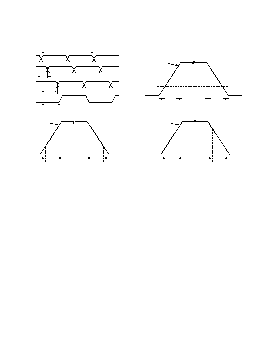
TIMING DIAGRAMS
CLK
t
CMOS
t
CLK
t
LVDS
t
PECL
05596-002
Figure 2. CLK/CLKB to Clock Output Timing, Divide = 1 Mode
05596-
099
DIFFERENTIAL
LVPECL
80%
20%
t
RP
t
FP
Figure 3. LVPECL Timing, Differential
DIFFERENTIAL
LVDS
80%
20%
t
RL
t
FL
05596-
003
Figure 4. LVDS Timing, Differential
SINGLE-ENDED
CMOS
3pF LOAD
80%
20%
t
RC
t
FC
05596-
004
Figure 5. CMOS Timing, Single-Ended, 3 pF Load
AD9514
Rev. 0 | Page 12 of 28
ABSOLUTE MAXIMUM RATINGS
Table 8.
Parameter or Pin
With
Respect
to
Min Max
Unit
VS
GND
-0.3
+3.6
V
RSET GND
-0.3
V
S
+ 0.3
V
CLK GND
-0.3
V
S
+ 0.3
V
CLK
CLKB
-1.2
+1.2
V
OUT0, OUT1, OUT2
GND
-0.3
V
S
+ 0.3
V
FUNCTION GND
-0.3
V
S
+ 0.3
V
STATUS GND
-0.3
V
S
+ 0.3
V
Junction Temperature
1
150
°C
Storage Temperature
-65
+150
°C
Lead Temperature (10 sec)
300
°C
Stresses above those listed under Absolute Maximum Ratings
may cause permanent damage to the device. This is a stress
rating only; functional operation of the device at these or any
other conditions above those indicated in the operational
section of this specification is not implied. Exposure to
absolute maximum ratings for extended periods may affect
device reliability.
THERMAL CHARACTERISTICS
2
Thermal Resistance
32-Lead LFCSP
3
JA
= 36.6°C/W
1
See Thermal Characteristics for .
JA
2
Thermal impedance measurements were taken on a 4-layer board in still air
in accordance with EIA/JESD51-7.
3
The external pad of this package must be soldered to adequate copper land
on board.
ESD CAUTION
ESD (electrostatic discharge) sensitive device. Electrostatic charges as high as 4000 V readily accumulate on
the human body and test equipment and can discharge without detection. Although this product features
proprietary ESD protection circuitry, permanent damage may occur on devices subjected to high energy
electrostatic discharges. Therefore, proper ESD precautions are recommended to avoid performance
degradation or loss of functionality.
AD9514
Rev. 0 | Page 13 of 28
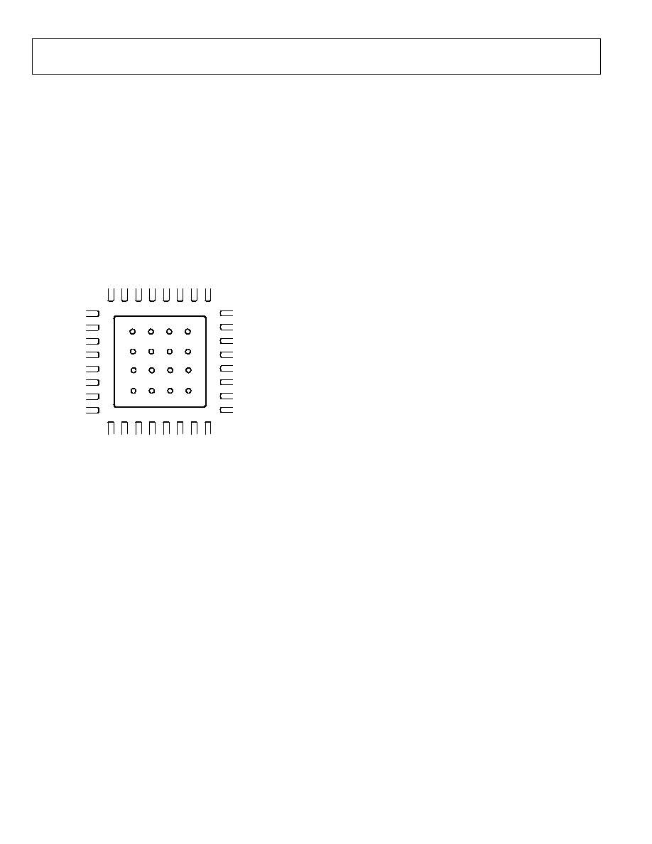
PIN CONFIGURATION AND FUNCTION DESCRIPTIONS
1
VS
2
CLK
3
CLKB
4
VS
5
SYNCB
6
VREF
7
S10
8
S9
18 OUT2B
19 OUT2
20 VS
21 VS
22 OUT1B
23 OUT1
24 VS
17 VS
9
S
8
1
0
S
7
1
1
S
6
1
3
S
4
1
5
S
2
1
4
S
3
1
6
S
1
1
2
S
5
2
6
V
S
2
7
O
U
T
0
B
2
8
O
U
T
0
2
9
V
S
3
0
V
S
2
5
S
0
TOP VIEW
(Not to Scale)
AD9514
3
1
G
N
D
3
2
R
S
E
T
05596-
005
Figure 6. 32-Lead LFCSP Pin Configuration
05596-
006
1
32
8
9
25
24
16
17
THE EXPOSED PADDLE
IS AN ELECTRICAL AND
THERMAL CONNECTION
EXPOSED PAD
(BOTTOM VIEW)
GND
Figure 7. Exposed Paddle
Note that the exposed paddle on this package is an electrical connection as well as a thermal enhancement. For the device to
function properly, the paddle must be soldered to a PCB land that functions as both a heat dissipation path as well as an electrical
ground (analog).
Table 9. Pin Function Descriptions
Pin No.
Mnemonic
Description
1, 4 ,17, 20, 21,
24, 26, 29, 30
VS
Power Supply (3.3 V).
2
CLK
Clock Input.
3
CLKB
Complementary Clock Input.
5
SYNCB
Used to Synchronize Outputs; Do Not Let Float.
6 VREF
Provides
2/3
V
S
for Use as One of the Four Logic Levels on S0 to S10.
7 to 16, 25
S10 to S0
Setup Select Pins. These are 4-state logic. The logic levels are V
S
, GND, 1/3 V
S
, and 2/3 V
S
.
The VREF pin provides 2/3 V
S
. Each pin is internally biased to 1/3 V
S
so that a pin requiring
that logic level should be left no connection (NC).
18
OUT2B
Complementary LVDS/Inverted CMOS Output.
19
OUT2
LVDS/CMOS Output.
22
OUT1B
Complementary LVPECL Output.
23 OUT1
LVPECL
Output.
27
OUT0B
Complementary LVPECL Output.
28 OUT0
LVPECL
Output.
31, Exposed Paddle
GND
Ground. The exposed paddle on the back of the chip is also GND.
32
RSET
Current Sets Resistor to Ground. Nominal value = 4.12 k.

AD9514
Rev. 0 | Page 14 of 28
TERMINOLOGY
Phase Jitter and Phase Noise
An ideal sine wave can be thought of as having a continuous
and even progression of phase with time from 0 to 360 degrees
for each cycle. Actual signals, however, display a certain amount
of variation from ideal phase progression over time. This
phenomenon is called phase jitter. Although there are many
causes that can contribute to phase jitter, one major component
is due to random noise that is characterized statistically as being
Gaussian (normal) in distribution.
This phase jitter leads to a spreading out of the energy of the
sine wave in the frequency domain, producing a continuous
power spectrum. This power spectrum is usually reported as a
series of values whose units are dBc/Hz at a given offset in
frequency from the sine wave (carrier). The value is a ratio
(expressed in dB) of the power contained within a 1 Hz
bandwidth with respect to the power at the carrier frequency.
For each measurement, the offset from the carrier frequency is
also given.
It is also meaningful to integrate the total power contained
within some interval of offset frequencies (for example, 10 kHz
to 10 MHz). This is called the integrated phase noise over that
frequency offset interval and can be readily related to the time
jitter due to the phase noise within that offset frequency
interval.
Phase noise has a detrimental effect on the performance of
ADCs, DACs, and RF mixers. It lowers the achievable dynamic
range of the converters and mixers, although they are affected
in somewhat different ways.
Time Jitter
Phase noise is a frequency domain phenomenon. In the
time domain, the same effect is exhibited as time jitter. When
observing a sine wave, the time of successive zero crossings is
seen to vary. For a square wave, the time jitter is seen as a
displacement of the edges from their ideal (regular) times of
occurrence. In both cases, the variations in timing from the
ideal are the time jitter. Since these variations are random in
nature, the time jitter is specified in units of seconds root mean
square (rms) or 1 sigma of the Gaussian distribution.
Time jitter that occurs on a sampling clock for a DAC or an
ADC decreases the SNR and dynamic range of the converter.
A sampling clock with the lowest possible jitter provides the
highest performance from a given converter.
Additive Phase Noise
It is the amount of phase noise that is attributable to the device
or subsystem being measured. The phase noise of any external
oscillators or clock sources has been subtracted. This makes it
possible to predict the degree to which the device affects the
total system phase noise when used in conjunction with the
various oscillators and clock sources, each of which contribute
their own phase noise to the total. In many cases, the phase
noise of one element dominates the system phase noise.
Additive Time Jitter
It is the amount of time jitter that is attributable to the device
or subsystem being measured. The time jitter of any external
oscillators or clock sources has been subtracted. This makes it
possible to predict the degree to which the device will affect the
total system time jitter when used in conjunction with the
various oscillators and clock sources, each of which contribute
their own time jitter to the total. In many cases, the time jitter of
the external oscillators and clock sources dominates the system
time jitter.
AD9514
Rev. 0 | Page 15 of 28
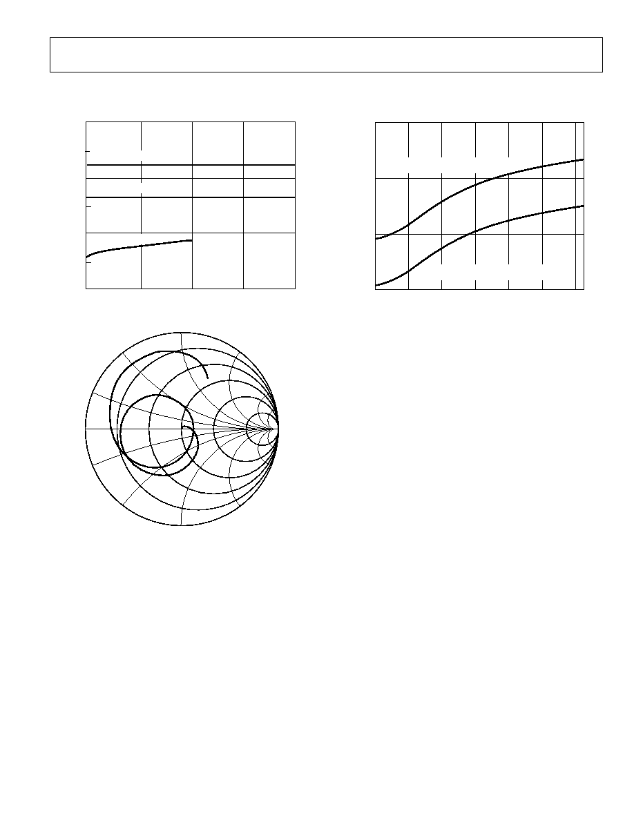
TYPICAL PERFORMANCE CHARACTERISTICS
OUTPUT FREQUENCY (MHz)
POWER (W)
1600
1200
800
400
05596-098
0.1
0.4
0.3
05596-098
2 LVPECL (DIV ON)
2 LVPECL (DIV = 1)
1 LVDS (DIV ON)
0.2
Figure 8. Power vs. Frequency--LVPECL, LVDS
START 300kHz
STOP 5GHz
05596-097
Figure 9. CLK Smith Chart (Evaluation Board)
OUTPUT FREQUENCY (MHz)
POWER (W)
120
100
80
40
20
0
60
0.3
0.6
0.5
0.4
05596-096
2 LVPECL (DIV ON) + 1 CMOS (DIV ON)
2 LVPECL (DIV OFF) + 1 CMOS (DIV OFF)
Figure 10. Power vs. Frequency--LVPECL, CMOS
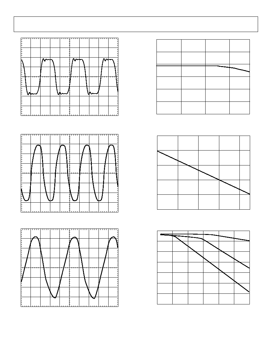
AD9514
Rev. 0 | Page 16 of 28
VERT 500mV/DIV
HORIZ 200ps/DIV
05596-
095
Figure 11. LVPECL Differential Output @ 1600 MHz
VERT 100mV/DIV
HORIZ 500ps/DIV
05596-
010
Figure 12. LVDS Differential Output @ 800 MHz
VERT 500mV/DIV
HORIZ 1ns/DIV
05596-
011
Figure 13. CMOS Single-Ended Output @ 250 MHz with 10 pF Load
OUTPUT FREQUENCY (MHz)
DI
FFE
RE
NTI
A
L S
WI
N
G (V
p-p)
100
1600
1100
600
1.2
1.3
1.4
1.5
1.6
1.7
1.8
05596-012
Figure 14. LVPECL Differential Peak-to-Peak Output Swing vs. Frequency
OUTPUT FREQUENCY (MHz)
DI
FFERENTI
A
L SWI
N
G
(
mV p-
p)
100
900
700
500
300
500
750
700
650
600
550
05596-013
Figure 15. LVDS Differential Peak-to-Peak Output Swing vs. Frequency
OUTPUT FREQUENCY (MHz)
OUT
P
UT
(V
PK
)
0
600
500
400
300
200
100
0
3.5
3.0
2.5
2.0
1.5
1.0
0.5
05596-014
2pF
10pF
20pF
Figure 16. CMOS Single-Ended Output Swing vs. Frequency and Load
AD9514
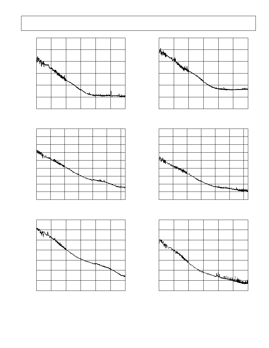
Rev. 0 | Page 17 of 28
OFFSET (Hz)
L
(f) (d
Bc/Hz)
10
10M
1M
100k
10k
1k
100
170
110
130
120
140
150
160
05596-015
Figure 17. Additive Phase Noise--LVPECL Divide = 1, 245.76 MHz
OFFSET (Hz)
L
(f) (d
Bc/Hz)
10
10M
1M
100k
10k
1k
100
170
80
90
110
100
120
130
140
150
160
05596-016
Figure 18. Additive Phase Noise--LVDS Divide = 1, 245.76 MHz
OFFSET (Hz)
L
(f) (d
Bc/Hz)
10
10M
1M
100k
10k
1k
100
170
100
110
120
130
140
150
160
05596-017
Figure 19. Additive Phase Noise--CMOS Divide = 1, 245.76 MHz
OFFSET (Hz)
L
(f) (d
Bc/Hz)
10
10M
1M
100k
10k
1k
100
170
110
130
120
140
150
160
05596-018
Figure 20. Additive Phase Noise--LVPECL Divide = 1, 622.08 MHz
OFFSET (Hz)
L
(f) (d
Bc/Hz)
10
10M
1M
100k
10k
1k
100
170
80
90
110
100
120
130
140
150
160
05596-019
Figure 21. Additive Phase Noise--LVDS Divide = 2, 122.88 MHz
OFFSET (Hz)
L
(f) (d
Bc/Hz)
10
10M
1M
100k
10k
1k
100
170
100
110
120
130
140
150
160
05596-020
Figure 22. Additive Phase Noise--CMOS Divide = 4, 61.44 MHz
AD9514
Rev. 0 | Page 18 of 28
FUNCTIONAL DESCRIPTION
OVERALL
The AD9514 provides for the distribution of its input clock
on up to three outputs simultaneously. OUT0 and OUT1 are
LVPECL levels. OUT2 can be set to either LVDS or CMOS
levels. Each output has its own divider that can be set for a
divide ratio selected from a list of integer values from 1
(bypassed) to 32.
OUT2 includes an analog delay block that can be set to add an
additional delay of 1.5 ns, 5 ns, or 10 ns full scale, each with
16 levels of fine adjustment.
CLK, CLKB--DIFFERENTIAL CLOCK INPUT
The CLK and CLKB pins are differential clock input pins.
This input works up to 1600 MHz. The jitter performance is
degraded by a slew rate below 1 V/ns. The input level should be
between approximately 150 mV p-p to no more than 2 V p-p.
Anything greater can result in turning on the protection diodes
on the input pins.
See Figure 23 for the CLK equivalent input circuit. This input
is fully differential and self-biased. The signal should be ac-
coupled using capacitors. If a single-ended input must be used,
this can be accommodated by ac coupling to one side of the
differential input only. The other side of the input should be
bypassed to a quiet ac ground by a capacitor.
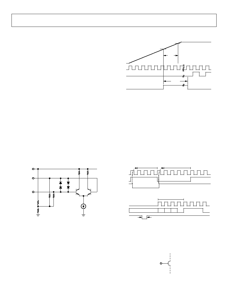
2.5k
5k
5k
2.5k
CLKB
CLK
V
S
CLOCK INPUT
STAGE
05596-
021
Figure 23 Clock Input Equivalent Circuit
SYNCHRONIZATION
Power-On SYNC
A power-on sync (POS) is issued when the V
S
power supply is
turned on to ensure that the outputs start in synchronization.
The power-on sync works only if the V
S
power supply transi-
tions the region from 2.2 V to 3.1 V within 35 ms. The POS can
occur up to 65 ms after V
S
crosses 2.2 V. Only outputs which are
not divide = 1 are synchronized.
05596-094
CLK
OUT
0V
3.3V
2.2V
3.1V
V
S
CLOCK FREQUENCY
IS EXAMPLE ONLY
DIVIDE = 2
PHASE = 0
< 65ms
INTERNAL SYNC NODE
35ms
MAX
Figure 24. Power-On Sync Timing
SYNCB
If the setup configuration of the AD9514 is changed during
operation, the outputs can become unsynchronized. The
outputs can be re-synchronized to each other at any time.
Synchronization occurs when the SYNCB pin is pulled low and
released. The clock outputs (except where divide = 1) are forced
into a fixed state (determined by the divide and phase settings)
and held there in a static condition until the SYNCB pin is
returned to high. Upon release of the SYNCB pin, after four
cycles of the clock signal at CLK, all outputs continue clocking
in synchronicity (except where divide = 1).
When divide = 1 for an output, that output is not affected by
SYNCB.
05596-
093
CLK
SYNCB
OUT
3 CLK CYCLES
4 CLK CYCLES
EXAMPLE: DIVIDE
8
PHASE = 0
EXAMPLE DIVIDE
RATIO PHASE = 0
Figure 25. SYNCB Timing with Clock Present
05596-
092
4 CLK CYCLES
CLK
OUT
SYNCB
DEPENDS ON PREVIOUS STATE AND DIVIDE RATIO
§
§
§
§
DEPENDS ON PREVIOUS STATE
EXAMPLE DIVIDE
RATIO PHASE = 0
MIN 5ns
Figure 26. SYNCB Timing with No Clock Present
The outputs of the AD9514 can be synchronized by using the
SYNCB pin. Synchronization aligns the phases of the clock
outputs, respecting any phase offset that has been set on a
particular output's divider.
SYNCB
05596-
022
Figure 27. SYNCB Equivalent Input Circuit
AD9514
Rev. 0 | Page 19 of 28
Synchronization is initiated by pulling the SYNCB pin low for a
minimum of 5 ns. The input clock does not have to be present
at the time the command is issued. The synchronization occurs
after four input clock cycles.
The synchronization applies to clock outputs:
·
that are not turned OFF
·
where the divider is not divide = 1 (divider bypassed)
An output with its divider set to divide = 1 (divider bypassed) is
always synchronized with the input clock, with a propagation
delay.
The SYNCB pin must be pulled up for normal operation. Do
not let the SYNCB pin float.
R
SET
RESISTOR
The internal bias currents of the AD9514 are set by the
R
SET
resistor. This resistor should be as close as possible to
the value given as a condition in the Specifications section
(R
SET
= 4.12 k). This is a standard 1% resistor value and
should be readily obtainable. The bias currents set by this
resistor determine the logic levels and operating conditions
of the internal blocks of the AD9514. The performance figures
given in the Specifications section assume that this resistor
value is used for R
SET
.
VREF
The VREF pin provides a voltage level of V
S
. This voltage is
one of the four logic levels used by the setup pins (S0 to S10).
These pins set the operation of the AD9514. The VREF pin
provides sufficient drive capability to drive as many of the setup
pins as necessary, up to all on a single part. The VREF pin
should be used for no other purpose.
SETUP CONFIGURATION
The specific operation of the AD9514 is set by the logic levels
applied to the setup pins (S0 to S10). These pins use four-state
logic. The logic levels used are V
S
and GND, plus V
S
and
V
S
. The V
S
level is provided by the internal self-biasing on
each of the setup pins (S0 to S10). This is the level seen by a
setup pin that is left not connected (NC). The V
S
level is
provided by the VREF pin. All setup pins requiring the V
S
level must be tied to the VREF pin.
SETUP PIN
S0 TO S10
60k
30k
V
S
05596-
023
Figure 28. Setup Pin (S0 to S10) Equivalent Circuit
The AD9514 operation is determined by the combination of
logic levels present at the setup pins. The setup configurations
for the AD9514 are shown in Table 10 to Table 15. The four
logic levels are referred to as 0, , , and 1. These numbers
represent the fraction of the V
S
voltage that defines the logic
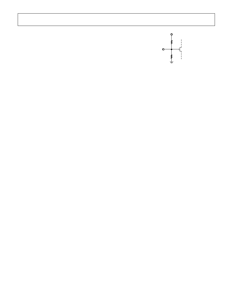
levels. See the setup pins thresholds in Table 6.
The meaning of some of the setup pins depends on the logic
level set on other pins. For example, the effect of the S3 to S4
pair of pins depends on whether S0 = 0. If S0 = 0, the delay
block for OUT2 is off, and the logic levels on S3 to S4 set the
phase word of the OUT2 divider. However, if S0 0, then the
full-scale delay for OUT2 is set by the logic level on S0, and S3
to S4 sets the delay block fine adjust (fraction of full scale).
S1 and S2 together determine the logic level of each output or
whether a channel is off. An output that is set to OFF is
powered down, including the divider.
OUT0 and OUT1 are LVPECL. The LVPECL output differential
voltage (V
OD
) can have three possible levels: 410 mV, 790 mV,
and 960 mV (limited to the available combinations, see Table 11).
OUT2 can be set to either LVDS or CMOS levels.
S5 and S6 effect depends on S2. If S2 = 0 (OUT2 is off), S5 and
S6 set the OUT1 phase word. If S2 0, S5 and S6 set the OUT2
divide ratio. If S2 = , then the value in S9 and S10 overrides
the divide ratio for OUT2.
S7 and S8 depend on S2 and S0. If S2 1, these pins set the
OUT1 divide ratio. However, if S2 = 1 (OUT1 is off) and S0 0,
S7 and S8 set the phase word for OUT2.
S9 and S10 depend on S2. If S2 , these pins set the OUT0
divide ratio. If S2 = , they set the OUT2 divide ratio,
overriding S5 and S6.
AD9514
Rev. 0 | Page 20 of 28
Table 10. S0--OUT2 Delay
S0
Delay Full Scale
0 Off
(Bypassed)
1/3 1.5
ns
2/3 5
ns
1 10
ns
Table 11. S1, S2--Output Select
S1 S2
OUT0
LVPECL
OUT1
LVPECL
OUT2
LVDS/CMOS
0 0 OFF
410
mV OFF
1/3
0
790 mV
790 mV
OFF
2/3
0
410 mV
410 mV
OFF
1 0 960
mV 960
mV OFF
0
1/3
790 mV
790 mV
CMOS
1/3 1/3 410
mV 410
mV LVDS
2/3 1/3 410
mV 410
mV CMOS
1
1/3
790 mV
790 mV
LVDS
0
2/3
OFF OFF OFF
1/3 2/3 OFF
OFF
LVDS
2/3 2/3 OFF
OFF
CMOS
1 2/3
OFF
790
mV OFF
0 1 410
mV OFF
CMOS
1/3 1 790
mV OFF
LVDS
2/3 1 410
mV OFF
LVDS
1 1 790
mV OFF
CMOS
Table 12. S3, S4--OUT2 Delay Fine Adjust or Phase
S0 0
S0 = 0
S3 S4
OUT2 Delay Fine Adjust
(Fraction of FS)
OUT2 Phase
0 0 0
0
1/3 0 1/16
1
2/3 0 1/8
2
1 0 3/16
3
0 1/3
1/4
4
1/3 1/3 5/16
5
2/3 1/3 3/8
6
1 1/3
7/16
7
0 2/3
1/2
8
1/3 2/3 9/16
9
2/3 2/3 5/8
10
1 2/3
11/16
11
0 1 3/4
12
1/3 1 13/16
13
2/3 1 7/8
14
1 1 15/16
15
AD9514
Rev. 0 | Page 21 of 28
Table 13. S5, S6--OUT2 Divide or OUT1 Phase
S2 0
S2 = 0
S5 S6
OUT2
Divide (Duty Cycle
1
)
OUT1
Phase
0 0 1
0
1/3 0 2
(50%)
1
2/3 0 3
(33%)
2
1 0 4
(50%)
3
0 1/3
5
(40%)
4
1/3 1/3 6
(50%)
5
2/3 1/3 8
(50%)
6
1 1/3
9
(44%)
7
0 2/3
10
(50%)
8
1/3 2/3 12
(50%)
9
2/3 2/3 15
(47%)
10
1 2/3
16
(50%)
11
0 1 18
(50%)
12
1/3 1 24
(50%)
13
2/3 1 30
(50%)
14
1 1 32
(50%)
15
1
Duty cycle is the clock signal high time divided by the total period.
Table 14. S7, S8--OUT1 Divide or OUT2 Phase
S2 1
S2 = 1 and S0 0
S7 S8
OUT1
Divide (Duty Cycle
1
)
OUT2
Phase
0 0 1
0
1/3 0 2
(50%)
1
2/3 0 3
(33%)
2
1 0 4
(50%)
3
0 1/3
5
(40%)
4
1/3 1/3 6
(50%)
5
2/3 1/3 8
(50%)
6
1 1/3
9
(44%)
7
0 2/3
10
(50%)
8
1/3 2/3 12
(50%)
9
2/3 2/3 15
(47%)
10
1 2/3
16
(50%)
11
0 1 18
(50%)
12
1/3 1 24
(50%)
13
2/3 1 30
(50%)
14
1 1 32
(50%)
15
1
Duty cycle is the clock signal high time divided by the total period.
Table 15. S9, S10--OUT0 Divide or OUT2 Divide
S2 2/3
S2 = 2/3
S9 S10
OUT0
Divide (Duty Cycle
1
)
OUT2
Divide (Duty Cycle
1
)
0
0
1
7 (43%)
1/3
0
2 (50%)
11 (45%)
2/3
0
3 (33%)
13 (46%)
1
0
4 (50%)
14 (50%)
0
1/3
5 (40%)
17 (47%)
1/3
1/3
6 (50%)
19 (47%)
2/3
1/3
8 (50%)
20 (50%)
1
1/3
9 (44%)
21 (48%)
0
2/3
10 (50%)
22 (50%)
1/3
2/3
12 (50%)
23 (48%)
2/3
2/3
15 (47%)
25 (48%)
1
2/3
16 (50%)
26 (50%)
0
1
18 (50%)
27 (48%)
1/3
1
24 (50%)
28 (50%)
2/3
1
30 (50%)
29 (48%)
1
1
32 (50%)
31 (48%)
1
Duty cycle is the clock signal high time divided by the total period.
AD9514
Rev. 0 | Page 22 of 28
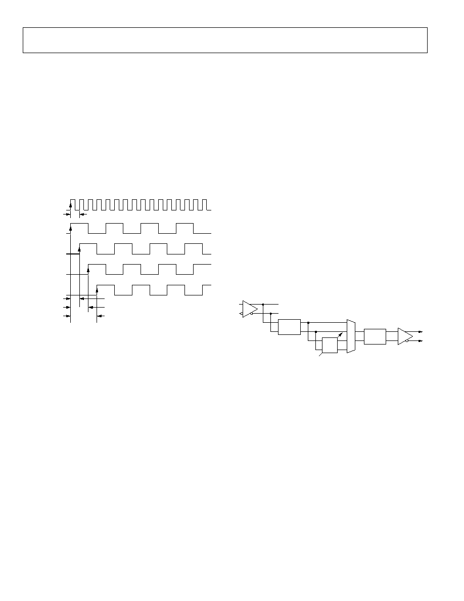
5
DIVIDER PHASE OFFSET
The phase of OUT1 or OUT2 can be selected, depending on the
divide ratio and output configuration chosen. This allows, for
example, the relative phase of OUT0 and OUT1 to be set.
After a SYNC operation (see the Synchronization section), the
phase offset word of each divider determines the number of
input clock (CLK) cycles to wait before initiating a clock output
edge. By giving each divider a different phase offset, output-to-
output delays can be set in increments of the fast clock period, t
CLK
.
Figure 29 shows four cases, each with the divider set to divide = 4.
By incrementing the phase offset from 0 to 3, the output is
offset from the initial edge by a multiple of t
CLK
.
0
1
4
1
2
3
5
9
6
7
8
10
14
11 12 13
t
CLK
CLOCK INPUT
CLK
DIVIDER OUTPUT
DIV = 4
PHASE = 0
PHASE = 1
PHASE = 2
PHASE = 3
t
CLK
2 × t
CLK
3 × t
CLK
05596-024
Figure 29. Phase Offset--Divider Set for Divide = 4, Phase Set from 0 to 2
For example:
CLK = 491.52 MHz
t
CLK
= 1/491.52 = 2.0345 ns
For Divide = 4:
Phase Offset 0 = 0 ns
Phase Offset 1 = 2.0345 ns
Phase Offset 2 = 4.069 ns
Phase Offset 3 = 6.104 ns
The outputs can also be described as:
Phase Offset 0 = 0°
Phase Offset 1 = 90°
Phase Offset 2 = 180°
Phase Offset 3 = 270°
Setting the phase offset to Phase = 4 results in the same relative
phase as Phase = 0° or 360°.
The resolution of the phase offset is set by the fast clock period
(t
CLK
) at CLK. The maximum unique phase offset is less than the
divide ratio, up to a phase offset of 15.
Phase offsets can be related to degrees by calculating the phase
step for a particular divide ratio:
Phase Step = 360°/Divide Ratio
Using some of the same examples:
Divide = 4
Phase Step = 360°/4 = 90°
Unique Phase Offsets in Degrees Are Phase = 0°, 90°,
180°, 270°
Divide = 9
Phase Step = 360°/9 = 40°
Unique Phase Offsets in Degrees Are Phase = 0°, 40°, 80°,
120°, 160°, 200°, 240°, 280°, 320°
DELAY BLOCK
OUT2 includes an analog delay element that gives variable time
delays (T) in the clock signal passing through that output.
÷
N
SELECT
LVDS
CMOS
T
MUX
OUTPUT
DRIVER
FINE DELAY ADJUST
(16 STEPS)
FULL SCALE : 1.5ns, 5ns, 10ns
CLOCK INPUT
OUT2 ONLY
05596-
025
Figure 30. Analog Delay Block
The amount of delay that can be used is determined by the
output frequency. The amount of delay is limited to less than
one-half cycle of the clock period. For example, for a 10 MHz
clock, the delay can extend to the full 10 ns maximum.
However, for a 100 MHz clock, the maximum delay is less than
5 ns (or half of the period).
The AD9514 allows for the selection of three full-scale delays,
1.5 ns, 5 ns, and 10 ns, set by delay full scale (see Table 10). Each
of these full-scale delays can be scaled by 16 fine adjustment
values, which are set by the delay word (see Table 12).
The delay block adds some jitter to the output. This means that
the delay function should be used primarily for clocking digital
chips, such as FPGA, ASIC, DUC, and DDC, rather than for
supplying a sample clock for data converters. The jitter is higher
for longer full scales because the delay block uses a ramp and
trip points to create the variable delay. A longer ramp means
more noise has a chance of being introduced.
AD9514
Rev. 0 | Page 23 of 28
When the delay block is OFF (bypassed), it is also powered
down.
OUTPUTS
The AD9514 offers three different output level choices:
LVPECL, LVDS, and CMOS. OUT0/OUT0B and OUT1/
OUT1B are LVPECL differential outputs. There are three
amounts of LVPECL differential voltage swing (V
OD
) that can be
selected (410 mV, 790 mV, and 960 mV) within the choices
available in Table 11.
OUT2/OUT2B can be selected as either an LVDS differential
output or a pair of CMOS single-ended outputs. If selected as
CMOS, OUT2 is a noninverted, single-ended output, and
OUT2B is an inverted, single-ended output.
GND
3.3V
OUTB
OUT
05596-
026
Figure 31. LVPECL Output Simplified Equivalent Circuit
OUTB
OUT
3.5mA
3.5mA
05596-
027
Figure 32. LVDS Output Simplified Equivalent Circuit
05596-
028
OUT2/
OUT2B
V
S
Figure 33. CMOS Equivalent Output Circuit
POWER SUPPLY
The AD9514 requires a 3.3 V ± 5% power supply for V
S
. The
tables in the Specifications section give the performance
expected from the AD9514 with the power supply voltage
within this range. In no case should the absolute maximum
range of -0.3 V to +3.6 V, with respect to GND, be exceeded
on Pin VS.
Good engineering practice should be followed in the layout of
power supply traces and the ground plane of the PCB. The
power supply should be bypassed on the PCB with adequate
capacitance (>10 F). The AD9514 should be bypassed with
adequate capacitors (0.1 F) at all power pins as close as
possible to the part. The layout of the AD9514 evaluation board
(AD9514/PCB) is a good example.
AD9514
Rev. 0 | Page 24 of 28
Exposed Metal Paddle
The exposed metal paddle on the AD9514 package is an
electrical connection, as well as a thermal enhancement. For the
device to function properly, the paddle must be properly
attached to ground (GND).
The exposed paddle of the AD9514 package must be soldered
down.
The AD9514 must dissipate heat through its exposed
paddle. The PCB acts as a heat sink for the AD9514. The PCB
attachment must provide a good thermal path to a larger heat
dissipation area, such as a ground plane on the PCB. This
requires a grid of vias from the top layer down to the ground
plane (see Figure 34). The AD9514 evaluation board
(AD9514/PCB) provides a good example of how the part
should be attached to the PCB.
05596-
035
VIAS TO GND PLANE
Figure 34. PCB Land for Attaching Exposed Paddle
POWER MANAGEMENT
In some cases the AD9514 can be configured to use less power
by turning off functions that are not being used.
The power-saving options include the following:
·
Any divider is powered down when set to divide = 1
(bypassed).
·
Adjustable delay block on OUT2 is powered down when in
off mode (S0 = 0).
·
In some cases, an unneeded output can be powered down
(see Table 11). This also powers down the divider for that
output.
AD9514
Rev. 0 | Page 25 of 28
APPLICATIONS
USING THE AD9514 OUTPUTS FOR ADC CLOCK
APPLICATIONS
Any high speed, analog-to-digital converter (ADC) is extremely
sensitive to the quality of the sampling clock provided by the
user. An ADC can be thought of as a sampling mixer, and any
noise, distortion, or timing jitter on the clock is combined with
the desired signal at the A/D output. Clock integrity require-
ments scale with the analog input frequency and resolution,
with higher analog input frequency applications at 14-bit
resolution being the most stringent. The theoretical SNR of an
ADC is limited by the ADC resolution and the jitter on the
sampling clock. Considering an ideal ADC of infinite resolution
where the step size and quantization error can be ignored, the
available SNR can be expressed approximately by
×
=
J
A
T
f
SNR
2
1
log
20
where f
A
is the highest analog frequency being digitized.
T
j
is the rms jitter on the sampling clock.
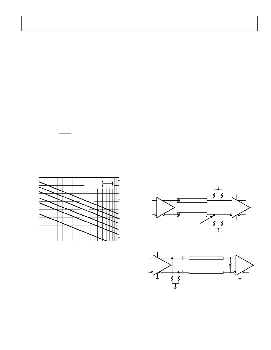
Figure 35 shows the required sampling clock jitter as a function
of the analog frequency and effective number of bits (ENOB).
f
A
FULL-SCALE SINE WAVE ANALOG FREQUENCY (MHz)
S
NR (dB)
EN
OB
10
1k
100
30
40
50
60
70
80
90
100
110
05596-091
6
8
10
12
14
16
18
T
J
= 100
f
S
200
f
S
400
f
S
1ps
2ps
10ps
SNR = 20log
1
2
f
A
T
J
Figure 35. ENOB and SNR vs. Analog Input Frequency
See Application Notes AN-756 and AN-501 at
www.analog.com
.
Many high performance ADCs feature differential clock inputs
to simplify the task of providing the required low jitter clock on
a noisy PCB. (Distributing a single-ended clock on a noisy PCB
can result in coupled noise on the sample clock. Differential
distribution has inherent common-mode rejection that can
provide superior clock performance in a noisy environment.)
The AD9514 features both LVPECL and LVDS outputs that
provide differential clock outputs, which enable clock solutions
that maximize converter SNR performance. The input
requirements of the ADC (differential or single-ended, logic
level, termination) should be considered when selecting the best
clocking/converter solution.
LVPECL CLOCK DISTRIBUTION
The low voltage, positive emitter-coupled, logic (LVPECL)
outputs of the AD9514 provide the lowest jitter clock signals
available from the AD9514. The LVPECL outputs (because they
are open emitter) require a dc termination to bias the output
transistors. The simplified equivalent circuit in Figure 31 shows
the LVPECL output stage.
In most applications, a standard LVPECL far-end termination is
recommended, as shown in Figure 36. The resistor network is
designed to match the transmission line impedance (50 ) and
the switching threshold (V
S
- 1.3 V).
V
S
LVPECL
50
50
SINGLE-ENDED
(NOT COUPLED)
V
S
V
S
LVPECL
127
127
83
83
V
T
= V
S
1.3V
05596-
030
Figure 36. LVPECL Far-End Termination
V
S
LVPECL
100
DIFFERENTIAL
(COUPLED)
V
S
LVPECL
100
0.1nF
0.1nF
200
200
05596-
031
Figure 37. LVPECL with Parallel Transmission Line
AD9514
Rev. 0 | Page 26 of 28
LVDS CLOCK DISTRIBUTION
Termination at the far end of the PCB trace is a second option.
The CMOS outputs of the AD9514 do not supply enough
current to provide a full voltage swing with a low impedance
resistive, far-end termination, as shown in Figure 40. The
far-end termination network should match the PCB trace
impedance and provide the desired switching point. The
reduced signal swing may still meet receiver input requirements
in some applications. This can be useful when driving long
trace lengths on less critical nets.
The AD9514 provides one clock output (OUT2) that is
selectable as either CMOS or LVDS levels. Low voltage
differential signaling (LVDS) is a differential output option for
OUT2. LVDS uses a current mode output stage. The current is
3.5 mA, which yields 350 mV output swing across a 100
resistor. The LVDS output meets or exceeds all ANSI/TIA/EIA-
644 specifications.
A recommended termination circuit for the LVDS outputs is
shown in Figure 38.
50
10
OUT2/OUT2B
SELECTED AS CMOS
V
S
CMOS
3pF
100
100
05596-
034
V
S
LVDS
100
DIFFERENTIAL (COUPLED)
V
S
LVDS
100
05596-
032
Figure 40. CMOS Output with Far-End Termination
Because of the limitations of single-ended CMOS clocking,
consider using differential outputs when driving high speed
signals over long traces. The AD9514 offers both LVPECL and
LVDS outputs that are better suited for driving long traces
where the inherent noise immunity of differential signaling
provides superior performance for clocking converters.
Figure 38. LVDS Output Termination
See Application Note AN-586 at
www.analog.com
for more
information on LVDS.
CMOS CLOCK DISTRIBUTION
SETUP PINS (S0 TO S10)
The AD9514 provides one output (OUT2) that is selectable as
either CMOS or LVDS levels. When selected as CMOS, this
output provides for driving devices requiring CMOS level logic
at their clock inputs.
The setup pins that require a logic level of V
S
(internal self-
bias) should be tied together and bypassed to ground via a
capacitor.
Whenever single-ended CMOS clocking is used, some of the
following general guidelines should be used.
The setup pins that require a logic level of V
S
should be tied
together, along with the VREF pin, and bypassed to ground via
a capacitor.
Point-to-point nets should be designed such that a driver has
only one receiver on the net, if possible. This allows for simple
termination schemes and minimizes ringing due to possible
mismatched impedances on the net. Series termination at the
source is generally required to provide transmission line
matching and/or to reduce current transients at the driver. The
value of the resistor is dependent on the board design and
timing requirements (typically 10 to 100 is used). CMOS
outputs are also limited in terms of the capacitive load or trace
length that they can drive. Typically, trace lengths less than
3 inches are recommended to preserve signal rise/fall times and
preserve signal integrity.
POWER AND GROUNDING CONSIDERATIONS AND
POWER SUPPLY REJECTION
Many applications seek high speed and performance under less
than ideal operating conditions. In these application circuits,
the implementation and construction of the PCB is as important
as the circuit design. Proper RF techniques must be used for
device selection, placement, and routing, as well as power
supply bypassing and grounding to ensure optimum
performance.
10
MICROSTRIP
GND
5pF
60.4
1.0 INCH
CMOS
05596-
033
Figure 39. Series Termination of CMOS Output
AD9514
Rev. 0 | Page 27 of 28
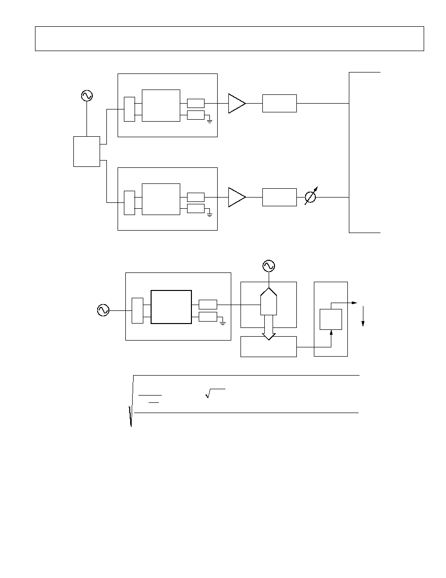
PHASE NOISE AND JITTER MEASUREMENT SETUPS
AD9514
CLK1
OUT1
OUT1B
BALUN
TERM
TERM
AMP
+28dB
ZFL1000VH2
ATTENUATOR
12dB
EVALUATION BOARD
AD9514
CLK1
OUT1
OUT1B
BALUN
TERM
TERM
AMP
+28dB
ZFL1000VH2
ATTENUATOR
7dB
SIG IN
REF IN
EVALUATION BOARD
WENZEL
OSCILLATOR
0
°
SPLITTER
ZESC-2-11
VARIABLE DELAY
COLBY PDL30A
0.01ns STEP
TO 10ns
AGILENT E5500B
PHASE NOI
SE MEASUREMENT SYSTEM
05596-041
Figure 41. Additive Phase Noise Measurement Configuration
AD9514
CLK1
OUT1
OUT1B
BALUN
TERM
CLK
ANALOG
SOURCE
TERM
EVALUATION BOARD
WENZEL
OSCILLATOR
WENZEL
OSCILLATOR
DATA CAPTURE CARD
FIFO
FFT
PC
ADC
SNR
t
J_RMS
05596-
042
Figure 42. Jitter Determination by Measuring SNR of ADC
(
)
(
)
[
]
2
2
2
2
2
2
20
2
10
A_PK
A
DNL
THERMAL
ON
QUANTIZATI
SNR
A_RMS
J_RMS
V
f
BW
SND
V
t
×
×
+
+
-
×
-
=
where:
t
j_RMS
is the rms time jitter.
SNR
is the signal-to-noise ratio.
SND
is the source noise density in nV/Hz.
BW
is the SND filter bandwidth.
V
A
is the analog source voltage.
f
A
is the analog frequency.
The terms are the quantization, thermal, and DNL errors.
AD9514
Rev. 0 | Page 28 of 28
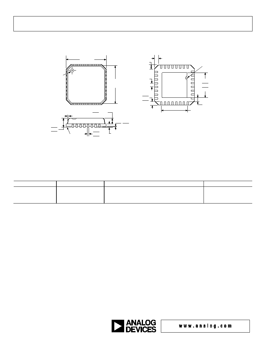
OUTLINE DIMENSIONS
COMPLIANT TO JEDEC STANDARDS MO-220-VHHD-2
0.30
0.23
0.18
0.20 REF
0.80 MAX
0.65 TYP
0.05 MAX
0.02 NOM
12° MAX
1.00
0.85
0.80
SEATING
PLANE
COPLANARITY
0.08
1
32
8
9
25
24
16
17
0.50
0.40
0.30
3.50 REF
0.50
BSC
PIN 1
INDICATOR
TOP
VIEW
5.00
BSC SQ
4.75
BSC SQ
3.25
3.10 SQ
2.95
PIN 1
INDICATOR
0.60 MAX
0.60 MAX
0.25 MIN
EXPOSED
PAD
(BOTTOM VIEW)
Figure 43. 32-Lead Lead Frame Chip Scale Package [LFCSP_VQ]
5 mm × 5 mm Body, Very Thin Quad (CP-32-2)
Dimensions shown in millimeters
ORDERING GUIDE
Model
Temperature Range
Package Description
Package Option
AD9514BCPZ
1
-40°C to +85°C
32-Lead Lead Frame Chip Scale Package (LFCSP_VQ)
CP-32-2
AD9514BCPZ-REEL7
1
-40°C to +85°C
32-Lead Lead Frame Chip Scale Package (LFCSP_VQ)
CP-32-2
AD9514/PCB
Evaluation
Board
1
Z = Pb-free part.
© 2005 Analog Devices, Inc. All rights reserved. Trademarks and
registered trademarks are the property of their respective owners.
D0559607/05(0)
Document Outline
- þÿ
- þÿ
- FUNCTIONAL BLOCK DIAGRAM
- þÿ
- þÿ
- þÿ
- þÿ
- þÿ
- þÿ
- TIMING CHARACTERISTICS
- þÿ
- þÿ
- SYNCB, VREF, AND SETUP PINS
- þÿ
- þÿ
- þÿ
- þÿ
- þÿ
- þÿ
- þÿ
- þÿ
- þÿ
- þÿ
- þÿ
- þÿ
- þÿ
- DIVIDER PHASE OFFSET
- þÿ
- þÿ
- þÿ
- þÿ
- þÿ
- þÿ
- LVDS CLOCK DISTRIBUTION
- þÿ
- þÿ
- þÿ
- PHASE NOISE AND JITTER MEASUREMENT SETUPS
- þÿ