Äîêóìåíòàöèÿ è îïèñàíèÿ www.docs.chipfind.ru
REV. E
Information furnished by Analog Devices is believed to be accurate and
reliable. However, no responsibility is assumed by Analog Devices for its
use, nor for any infringements of patents or other rights of third parties that
may result from its use. No license is granted by implication or otherwise
under any patent or patent rights of Analog Devices.
a
AD9432
One Technology Way, P.O. Box 9106, Norwood, MA 02062-9106, U.S.A.
Tel: 781/329-4700
www.analog.com
Fax: 781/326-8703
© Analog Devices, Inc., 2002
12-Bit, 80 MSPS/105 MSPS
A/D Converter
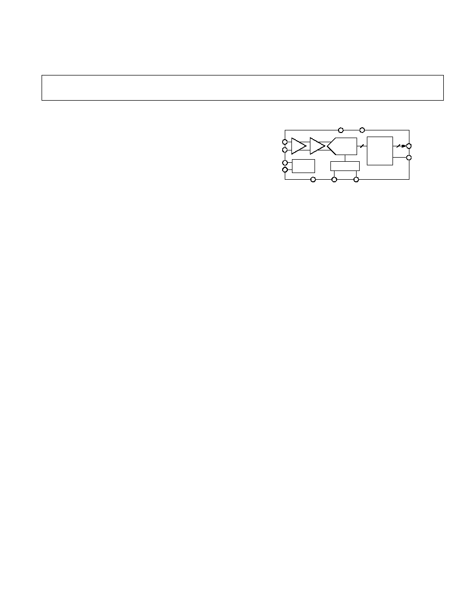
FUNCTIONAL BLOCK DIAGRAM
12
AIN
ENCODE
12
AD9432
GND
VREFOUT
D11D0
VREFIN
AIN
ENCODE
V
CC
V
DD
TIMING
REF
OUTPUT
STAGING
PIPELINE
ADC
BUF
T/H
OR
FEATURES
On-Chip Reference and Track/Hold
On-Chip Input Buffer
850 mW Typical Power Dissipation at 105 MSPS
500 MHz Analog Bandwidth
SNR = 67 dB @ 49 MHz AIN at 105 MSPS
SFDR = 80 dB @ 49 MHz AIN at 105 MSPS
2.0 V p-p Differential Analog Input Range
Single 5.0 V Supply Operation
3.3 V CMOS/TTL Outputs
Two's Complement Output Format
APPLICATIONS
Communications
Basestations and `Zero-IF' Subsystems
Wireless Local Loop (WLL)
Local Multipoint Distribution Service (LMDS)
HDTV Broadcast Cameras and Film Scanners
GENERAL INTRODUCTION
The AD9432 is a 12-bit monolithic sampling analog-to-digital
converter with an on-chip track-and-hold circuit and is optimized
for high-speed conversion and ease of use. The product operates
at a 105 MSPS conversion rate with outstanding dynamic per-
formance over its full operating range.
The ADC requires only a single 5.0 V power supply and a
105 MHz encode clock for full-performance operation. No
external reference or driver components are required for many
applications. The digital outputs are TTL/CMOS compatible
and a separate output power supply pin supports interfacing
with 3.3 V logic. The encode input supports either differential
or single-ended and is TTL/CMOS-compatible.
Fabricated on an advanced BiCMOS process, the AD9432 is
available in a 52-lead plastic quad flatpack package (LQFP)
specified over the industrial temperature range (40
°C to +85°C).

REV. E
2
AD9432SPECIFICATIONS
Test
AD9432BST/BSQ-80
AD9432BST/BSQ-105
Parameter
Temp
Level
Min
Typ
Max
Min
Typ
Max
Unit
RESOLUTION
12
12
Bits
DC ACCURACY
Differential Nonlinearity
25
°C
I
0.75
±0.25
+0.75
0.75
±0.25
+0.75
LSB
Full
VI
1.0
±0.5
+1.0
1.0
±0.5
+1.0
LSB
Integral Nonlinearity
25
°C
I
1.0
±0.5
+1.0
1.0
±0.5
+1.0
LSB
Full
VI
1.5
±1.0
+1.5
1.5
±1.0
+1.5
LSB
No Missing Codes
Full
VI
Guaranteed
Guaranteed
Gain Error
1
25
°C
I
5
+2
+7
5
+2
+7
% FS
Gain Tempco
1
Full
V
150
150
ppm/
°C
ANALOG INPUT
Input Voltage Range (AIN
AIN)
Full
V
±1.0
±1.0
V
Common-Mode Voltage
Full
V
3.0
3.0
V
Input Offset Voltage
Full
VI
5
±0
+5
5
±0
+5
mV
Input Resistance
Full
VI
2
3
4
2
3
4
k
Input Capacitance
25
°C
V
4
4
pF
Analog Bandwidth, Full Power
25
°C
V
500
500
MHz
ANALOG REFERENCE
Output Voltage
Full
VI
2.4
2.5
2.6
2.4
2.5
2.6
V
Tempco
Full
V
50
50
ppm/
°C
Input Bias Current
Full
VI
15
50
15
50
µ
SWITCHING PERFORMANCE
Maximum Conversion Rate
Full
VI
80
105
MSPS
Minimum Conversion Rate
Full
IV
1
1
MSPS
Encode Pulsewidth High (t
EH
)
25
°C
IV
4.0
6.2
4.0
4.8
ns
Encode Pulsewidth Low (t
EL
)
25
°C
IV
4.0
6.2
4.0
4.8
ns
Aperture Delay (t
A
)
25
°C
V
2.0
2.0
ns
Aperture Uncertainty (Jitter)
25
°C
V
0.25
0.25
ps rms
Output Valid Time (t
V
)
2
Full
VI
3.0
5.3
3.0
5.3
ns
Output Propagation Delay (t
PD
)
2
Full
VI
5.5
8.0
5.5
8.0
ns
Output Rise Time (t
R
)
2
Full
V
2.1
2.1
ns
Output Fall Time (t
F
)
Full
V
1.9
1.9
ns
Out-of-Range Recovery Time
25
°C
V
2
2
ns
Transient Response Time
25
°C
V
2
2
ns
Latency
Full
IV
10
10
Cycles
DIGITAL INPUTS
Encode Input Common Mode
Full
V
1.6
1.6
V
Differential Input (ENC
ENC)
Full
V
750
750
mV
Single-Ended
Logic "1" Voltage
Full
IV
2.0
2.0
V
Logic "0" Voltage
Full
IV
0.8
0.8
V
Input Resistance
Full
VI
3
5
8
3
5
8
k
Input Capacitance
25
°C
V
4.5
4.5
pF
DIGITAL OUTPUTS
Logic "1" Voltage (V
DD
= 3.3 V)
Full
VI
V
DD
0.05
V
DD
0.05
V
Logic "0" Voltage (V
DD
= 3.3 V)
Full
VI
0.05
0.05
V
Output Coding
Two's Complement
Two's Complement
POWER SUPPLY
Power Dissipation
3
Full
VI
790
1000
850
1100
mW
Power Supply Rejection Ratio (PSRR) 25
°C
I
5
+0.5
+5
5
+0.5
+5
mV/V
I
VCC
Full
VI
158
200
170
220
mA
I
VDD
Full
VI
9.5
12.2
12.5
16
mA
(V
DD
= 3.3 V, V
CC
= 5.0 V; external reference; differential encode input, unless
otherwise noted.)

REV. E
3
AD9432
Test
AD9432BST/BSQ-80
AD9432BST/BSQ-105
Parameter
Temp
Level
Min
Typ
Max
Min
Typ
Max
Unit
DYNAMIC PERFORMANCE
4
Signal-to-Noise Ratio (SNR)
(Without Harmonics)
f
IN
= 10.3 MHz
25
°C
I
65.5
67.5
65.5
67.5
dB
f
IN
= 40 MHz
25
°C
I
65
67.2
67.2
dB
f
IN
= 49 MHz
25
°C
I
67.0
64
67.0
dB
f
IN
= 70 MHz
25
°C
V
66.1
66.1
dB
Signal-to-Noise Ratio (SINAD)
(With Harmonics)
f
IN
= 10.3 MHz
25
°C
I
65
67.2
65
67.2
dB
f
IN
= 40 MHz
25
°C
I
64.5
66.9
66.9
dB
f
IN
= 49 MHz
25
°C
I
66.7
63
66.7
dB
f
IN
= 70 MHz
25
°C
V
65.8
65.8
dB
Effective Number of Bits
f
IN
= 10 MHz
25
°C
V
11.0
11.0
Bits
f
IN
= 40 MHz
25
°C
V
10.9
10.9
Bits
f
IN
= 49 MHz
25
°C
V
10.9
10.9
Bits
f
IN
= 70 MHz
25
°C
V
10.7
10.7
Bits
Second and Third Harmonic Distortion
f
IN
= 10 MHz
25
°C
I
75
85
75
85
dBc
f
IN
= 40 MHz
25
°C
I
73
85
83
dBc
f
IN
= 49 MHz
25
°C
I
83
72
80
dBc
f
IN
= 70 MHz
25
°C
V
80
78
dBc
Worst Harmonic or Spur
(Excluding Second and Third)
f
IN
= 10 MHz
25
°C
I
80
90
80
90
dBc
f
IN
= 40 MHz
25
°C
I
80
90
90
dBc
f
IN
= 49 MHz
25
°C
I
90
80
90
dBc
f
IN
= 70 MHz
25
°C
V
90
90
dBc
Two-Tone Intermod Distortion (IMD)
f
IN1
= 29.3 MHz; f
IN2
= 30.3 MHz
25
°C
V
75
75
dBc
f
IN1
= 70.3 MHz; f
IN2
= 71.3 MHz
25
°C
V
66
66
dBc
NOTES
1
Gain error and gain temperature coefficients are based on the ADC only (with a fixed 2.5 V external reference and a 2 V p-p differential analog input).
2
t
V
and t
PD
are measured from the transition points of the ENCODE input to the 50%/50% levels of the digital outputs swing. The digital output load during test is
not to exceed an ac load of 10 pF or a dc current of
±40 µA. Rise and fall times measured from 10% to 90%.
3
Power dissipation measured with encode at rated speed and a dc analog input. (Outputs Static, I
VDD
= 0.)
4
SNR/harmonics based on an analog input voltage of 0.5 dBFS referenced to a 2 V full-scale input range.
Specifications subject to change without notice.
REV. E
AD9432
4
ABSOLUTE MAXIMUM RATINGS
*
V
DD
. . . . . . . . . . . . . . . . . . . . . . . . . . . . . . . . . . . . . . . . . . 6 V
V
CC
. . . . . . . . . . . . . . . . . . . . . . . . . . . . . . . . . . . . . . . . . . 6 V
Analog Inputs . . . . . . . . . . . . . . . . . . . 0.5 V to V
CC
+ 0.5 V
Digital Inputs . . . . . . . . . . . . . . . . . . . 0.5 V to V
DD
+ 0.5 V
VREFIN . . . . . . . . . . . . . . . . . . . . . . . 0.5 V to V
CC
+ 0.5 V
Digital Output Current . . . . . . . . . . . . . . . . . . . . . . . . 20 mA
Operating Temperature . . . . . . . . . . . . . . . . 55
°C to +125°C
Storage Temperature . . . . . . . . . . . . . . . . . . 65
°C to +150°C
Maximum Junction Temperature . . . . . . . . . . . . . . . . 150
°C
Maximum Case Temperature . . . . . . . . . . . . . . . . . . . 150
°C
*Stresses above those listed under Absolute Maximum Ratings may cause perma-
nent damage to the device. This is a stress rating only; functional operation of the
device at these or any other conditions outside of those indicated in the operation
sections of this specification is not implied. Exposure to absolute maximum
ratings for extended periods may affect device reliability.
CAUTION
ESD (electrostatic discharge) sensitive device. Electrostatic charges as high as 4000 V readily
accumulate on the human body and test equipment and can discharge without detection.
Although the AD9432 features proprietary ESD protection circuitry, permanent damage may
occur on devices subjected to high-energy electrostatic discharges. Therefore, proper ESD
precautions are recommended to avoid performance degradation or loss of functionality.
WARNING!
ESD SENSITIVE DEVICE
PowerQuad is a registered trademark of AMkor Technology, Inc.
THERMAL CHARACTERISTICS
52-Lead Plastic LQFP (ST-52)
JA
= 50
°C/W, No Airflow
52-lead PowerQuad
®
4 LQFP (SQ-52)
JA
= 25
°C/W, Soldered Exposed Heat Sink, No Airflow
JA
= 33
°C/W, Unsoldered Exposed Heat Sink, No Airflow
JC
= 2
°C/W, Bottom of package (Exposed Heat Sink)
Simulated Typical performance for 4-layer JEDEC board,
horizontal orientation.
ORDERING GUIDE
Temperature
Package
Package
Model
Ranges
Descriptions
Option
AD9432BSQ
40
°C to +85°C 52-Lead Thermally
SQ-52
-80, -105
Enhanced Plastic
Quad Flatpack
AD9432BST
40
°C to +85°C 52-Lead Plastic Quad ST-52
-80, -105
Flatpack (LQFP)
AD9432/PCB 25
°C
Evaluation Board
EXPLANATION OF TEST LEVELS
Test Level
I
100% production tested.
II
100% production tested at 25
°C and sample tested at
specified temperatures.
III Sample tested only.
IV Parameter is guaranteed by design and characterization
testing.
V
Parameter is a typical value only.
VI 100% production tested at 25
°C; guaranteed by design and
characterization testing for industrial temperature range.
REV. E
AD9432
5
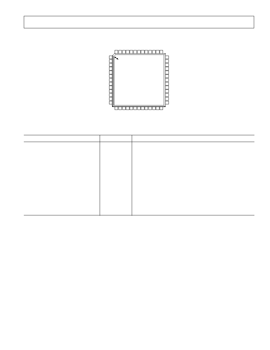
PIN CONFIGURATION
52 51 50 49 48
43 42 41 40
47 46 45 44
14 15 16 17 18 19 20 21 22 23 24 25 26
1
2
3
4
5
6
7
8
9
10
11
13
12
PIN 1
IDENTIFIER
TOP VIEW
(Not to Scale)
39
38
37
36
35
34
33
32
31
30
29
28
27
GND
GND
GND
OR
AD9432
GND
V
CC
V
CC
GND
GND
GND
V
DD
DGND
D0 (LSB)
D1
D2
D3
V
CC
GND
GND
V
CC
V
CC
ENCODE
ENCODE
GND
V
CC
GND
DGND
V
DD
(MSB) D11
D10
D9
D8
D7
D6
DGND
V
DD
V
DD
DGND
D5
D4
DNC
V
CC
GND
VREFIN
VREFOUT
V
CC
AIN
AIN
GND
GND
V
CC
V
CC
DEFINITION OF SPECIFICATIONS
Analog Bandwidth (Small Signal)
The analog input frequency at which the spectral power of the
fundamental frequency (as determined by the FFT analysis) is
reduced by 3 dB.
Aperture Delay
The delay between a differential crossing of ENCODE and
ENCODE and the instant at which the analog input is sampled.
Aperture Uncertainty (Jitter)
The sample-to-sample variation in aperture delay.
Differential Nonlinearity
The deviation of any code from an ideal 1 LSB step.
Encode Pulsewidth/Duty Cycle
Pulsewidth high is the minimum amount of time that the ENCODE
pulse should be left in Logic "1" state to achieve rated performance;
pulsewidth low is the minimum time ENCODE pulse should be left
in low state. At a given clock rate, these specs define an acceptable
Encode duty cycle.
Integral Nonlinearity
The deviation of the transfer function from a reference line
measured in fractions of 1 LSB using a "best straight line"
determined by a least square curve fit.
Minimum Conversion Rate
The encode rate at which the SNR of the lowest analog signal
frequency drops by no more than 3 dB below the guaranteed limit.
Maximum Conversion Rate
The encode rate at which parametric testing is performed.
Output Propagation Delay
The delay between a differential crossing of ENCODE and
ENCODE and the time when all output data bits are within
valid logic levels.
Power Supply Rejection Ratio
The ratio of a change in input offset voltage to a change in
power supply voltage.
Signal-to-Noise Plus Distortion (SINAD)
The ratio of the rms signal amplitude (set at 1 dB below full
scale) to the rms value of the sum of all other spectral compo-
nents, including harmonics but excluding dc.
Signal-to-Noise Ratio (SNR)
The ratio of the rms signal amplitude (set at 1 dB below full
scale) to the rms value of the sum of all other spectral compo-
nents, excluding the first five harmonics and dc.
PIN FUNCTION DESCRIPTIONS
Pin Number (AD9432BST)
Mnemonic
Function
1, 3, 4, 9, 11, 33, 34, 35, 38, 39, 40, 43, 48, 51
GND
Analog Ground
2, 5, 6, 10, 36, 37, 42, 44, 47, 52
V
CC
Analog Supply (5 V)
7
ENCODE
Encode Clock for ADCComplementary
8
ENCODE
Encode Clock for ADCTrue (ADC samples on rising edge of ENCODE)
14
OR
Out of Range Output
1520, 2530
D11D6, D5D0 Digital Output
12, 21, 24, 31
DGND
Digital Output Ground
13, 22, 23, 32
V
DD
Digital Output Power Supply (2.7 V to 3.6 V)
41
DNC
Do Not Connect
45
VREFIN
Reference Input for ADC (2.5 V Typical); Bypass with 0.1
µF to Ground.
46
VREFOUT
Internal Reference Output (2.5 V Typical)
49
AIN
Analog InputTrue
50
AIN
Analog InputComplementary
REV. E
AD9432
6
Spurious-Free Dynamic Range (SFDR)
The ratio of the rms signal amplitude to the rms value of the
peak spurious spectral component. The peak spurious compo-
nent may or may not be a harmonic. May be reported in dBc
(i.e., degrades as signal level is lowered), or in dBFS (always
related back to converter full scale).
Two-Tone Intermodulation Distortion Rejection
The ratio of the rms value of either input tone to the rms value
of the worst third order intermodulation product; reported in dBc.
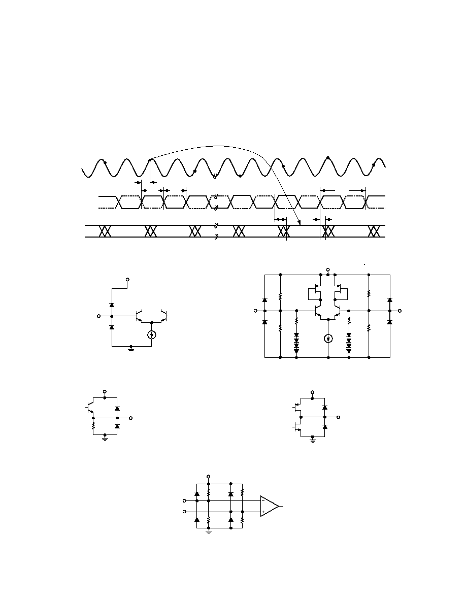
t
PD
t
A
AIN
ENCODE
ENCODE
D11D0
SAMPLE N1
SAMPLE N
SAMPLE N+10
SAMPLE N+11
SAMPLE N+9
SAMPLE N+1
t
EH
t
EL
1/f
S
DATA N11
DATA N10
N9
DATA N1
DATA N
DATA N + 1
t
V
N2
Figure 1. Timing Diagram
V
CC
VREFIN
Figure 2. Equivalent Voltage Reference Input Circuit
V
CC
VREFOUT
Q1
NPN
V
REF
OUTPUT
Figure 3. Equivalent Voltage Reference Output Circuit
Two-Tone SFDR
The ratio of the rms value of either input tone to the rms value
of the peak spurious component. The peak spurious component
may or may not be an IMD product. May be reported in dBc
(i.e., degrades as signal level is lowered), or in dBFS (always
related back to converter full scale).
Worst Harmonic
The ratio of the rms signal amplitude to the rms value of the
worst harmonic component, reported in dBc.
V
CC
17k
8k
100
100
17k
8k
ENCODE
ENCODE
Figure 4. Equivalent Encode Input Circuit
V
DD
DIGITAL
OUTPUT
DIGITAL OUTPUT
Figure 5. Equivalent Digital Output Circuit
V
CC
5k
5k
7k
7k
AIN
AIN
ANALOG INPUT
Figure 6. Equivalent Analog Input Circuit
REV. E
AD9432
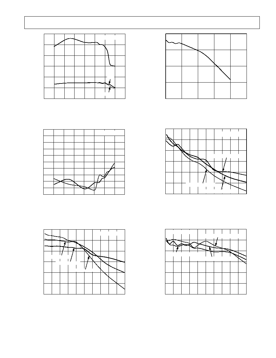
7
ENCODE MSPS
90
0
20
dB
40
60
80
100
120
140
160
85
80
75
70
65
60
AIN = 10.3MHz
SINAD
SFDR
SNR
TPC 1. SNR/SINAD/SFDR vs. f
S
: f
IN
= 10.3 MHz
ENCODE MSPS
0
20
dBc
40
60
80
100
120
140
160
90
95
100
85
80
75
70
65
60
55
50
AIN = 10.3MHz
2nd
3rd
TPC 2. Harmonics vs. f
S
: f
IN
= 10.3 MHz
ANALOG INPUT FREQUENCY MHz
70
0
20
dB
40
60
80
100
120
140
160
200
65
60
55
50
45
40
ENCODE = 105MSPS
SINAD (0.5dBFS)
SINAD (3.0dBFS)
SINAD (6.0dBFS)
180
TPC 3. SINAD vs. f
IN
: f
S
= 105 MSPS
AIN INPUT FREQUENCY MHz (0.5dBFS)
70
0
SNR
dB
50
100
150
200
250
65
60
55
50
TPC 4. SNR vs. AIN Input Frequency,
Encode = 105 MSPS
ANALOG INPUT FREQUENCY MHz
0
100
dBc
20
120
40
140
60
160
80
50
40
60
70
80
90
100
180
2nd or 3rd (3.0dBFS)
2nd or 3rd (6.0dBFS)
2nd or 3rd (0.5dBFS)
200
ENCODE = 105MSPS
TPC 5. Harmonics vs. f
IN
: f
S
= 105 MSPS
ANALOG INPUT FREQUENCY MHz
0
20
dBc
40
60
80
100
120
140
160
50
40
60
70
80
90
100
180
200
WORST OTHER (3.0dBFS)
WORST OTHER (6.0dBFS)
WORST OTHER (0.5dBFS)
ENCODE = 105MSPS
TPC 6. Worst-Case Spur (Other than Second and
Third) vs. f
IN
: f
S
= 105 MSPS
Typical Performance Characteristics
REV. E
AD9432
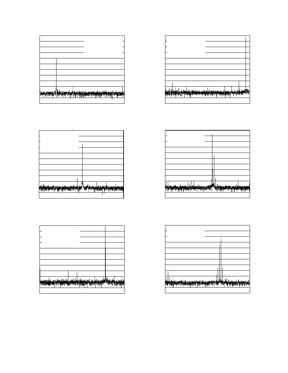
8
dB
SAMPLES
80
90
100
70
60
50
40
30
20
10
0
110
120
ENCODE = 105MSPS
AIN = 10.3MHz (0.53dBFS)
SNR = 67.32dB
SINAD = 67.07dB
SFDR = 85dBc
TPC 7. Spectrum: f
S
= 105 MSPS, f
IN
= 10.3 MHz
SAMPLES
dB
80
90
100
70
60
50
40
30
20
10
0
110
120
ENCODE = 105MSPS
AIN = 27.0MHz (0.52dBFS)
SNR = 67.3dB
SINAD = 67.0dB
SFDR = 83.1dBc
TPC 8. Spectrum: f
S
= 105 MSPS, f
IN
= 27 MHz
SAMPLES
dB
80
90
100
70
60
50
40
30
20
10
0
110
120
ENCODE = 105MSPS
AIN = 40.9MHz (0.56dBFS)
SNR = 67.2dB
SINAD = 66.9dB
SFDR = 80dBc
TPC 9. Spectrum: f
S
= 105 MSPS, f
IN
= 40.9 MHz
SAMPLES
dB
80
90
100
70
60
50
40
30
20
10
0
110
120
ENCODE = 105MSPS
AIN = 50.3MHz (0.46dBFS)
SNR = 67.0dB
SINAD = 66.7dB
SFDR = 80dBc
TPC 10. Spectrum: f
S
= 105 MSPS, f
IN
= 50.3 MHz
SAMPLES
dBc
80
90
100
70
60
50
40
30
20
10
0
110
120
AIN1 = 29.3MHz (7dBFS)
AIN2 = 30.3MHz (7dBFS)
ENCODE = 105MSPS
TPC 11. Two-Tone Spectrum, Wideband: f
S
=
105 MSPS, AIN1 = 29.3 MHz, AIN2 = 30.3 MHz
SAMPLES
dBc
80
90
100
70
60
50
40
30
20
10
0
110
120
AIN1 = 70.3MHz (7dBFS)
AIN2 = 71.3MHz (7dBFS)
ENCODE = 105MSPS
TPC 12. Two-Tone Spectrum, Wideband: f
S
=
105 MSPS, AIN1 = 70.3 MHz, AIN2 = 71.3 MHz
REV. E
AD9432
9
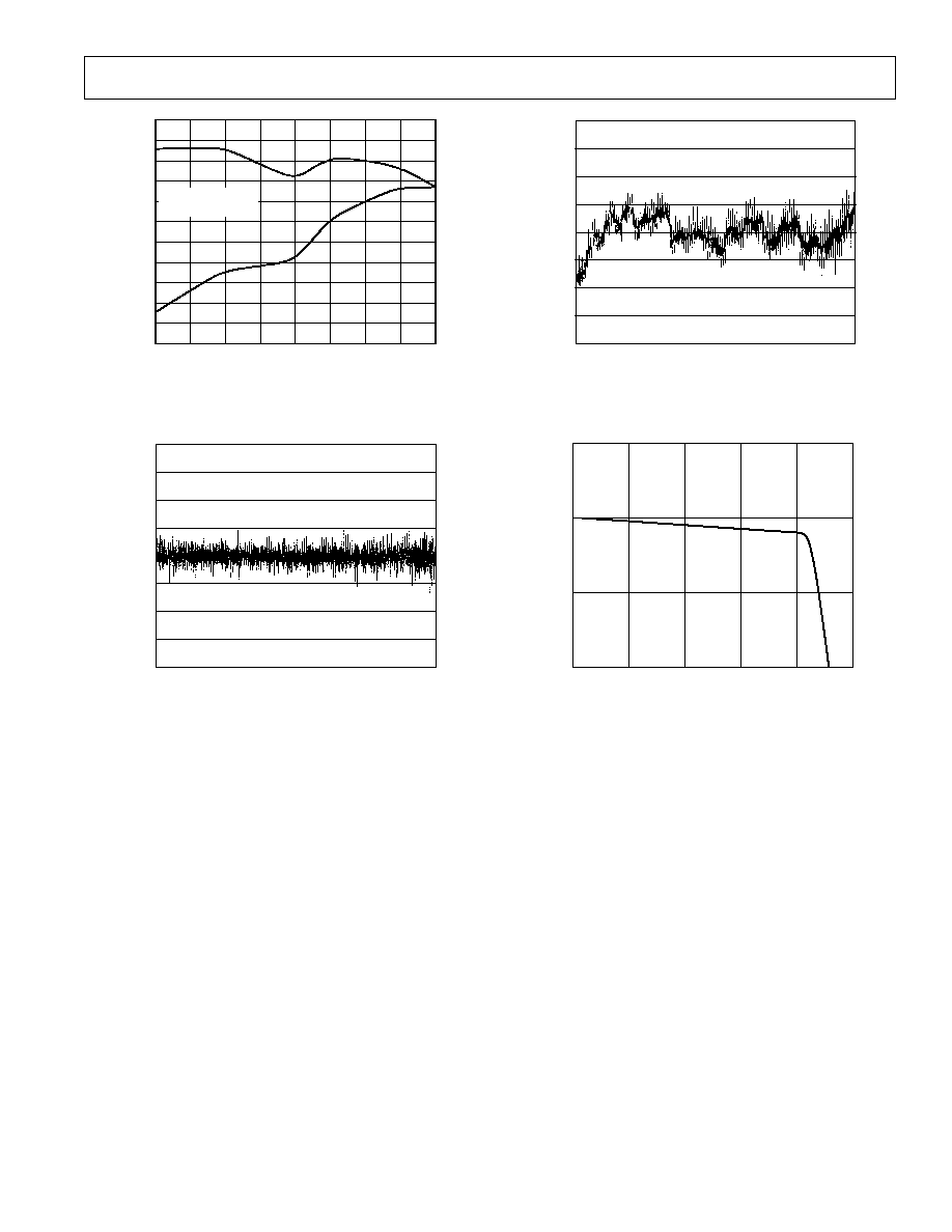
ANALOG INPUT POWER LEVEL dBFS
80
70
WORST-CASE SPURIOUS
dBc AND dBFS
60
40
30
20
10
50
40
60
70
80
90
100
110
30
20
10
0
50
0
dBFS
dBc
ENCODE = 105MSPS
AIN = 50.3MHz
TPC 13. Single Tone SFDR
LSB
DNL
0.50
0.75
0.25
0.00
0.25
0.50
0.75
1.00
1.00
TPC 14. Differential Nonlinearity: f
S
= 105 MSPS
LSB
INL
0.50
0.75
0.25
0.00
0.25
0.50
0.75
1.00
1.00
TPC 15. Integral Nonlinearity: f
S
= 105 MSPS
CURRENT mA
0
2
VOLTAGE
V
4
8
10
2.0
2.5
3.0
1.5
6
TPC 16. Voltage Reference Output vs. Current Load
REV. E
AD9432
10
APPLICATION NOTES
Theory of Operation
The AD9432 is a multibit pipeline converter that uses a switched
capacitor architecture. Optimized for high speed, this converter
provides flat dynamic performance up to frequencies near Nyquist.
DNL transitional errors are calibrated at final test to a typical
accuracy of 0.25 LSB or less.
USING THE AD9432
Analog Input
The analog input to the AD9432 is a differential buffer. The input
buffer is self-biased by an on-chip resistor divider that sets the
dc common-mode voltage to a nominal 3 V (see Equivalent
Circuits section). Rated performance is achieved by driving the
input differentially. Minimum input offset voltage is obtained when
driving from a source with a low differential source impedance
such as a transformer in ac applications. Capacitive coupling at the
inputs will increase the input offset voltage by as much as
±25 mV.
Driving the ADC single-endedly will degrade performance.
For best dynamic performance, impedances at AIN and
AIN
should match.
Special care was taken in the design of the analog input section
of the AD9432 to prevent damage and corruption of data when
the input is overdriven. The nominal input range is 2 V p-p.
Each analog input will be 1 V p-p when driven differentially.
2.5
3.5
4.0
2.0
3.0
AIN
AIN
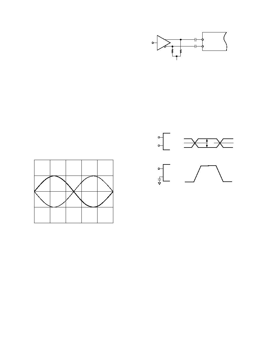
Figure 7. Full-Scale Analog Input Range
ENCODE Input
Any high speed A/D converter is extremely sensitive to the qual-
ity of the sampling clock provided by the user. A track/hold
circuit is essentially a mixer, and any noise, distortion, or timing
jitter on the clock will be combined with the desired signal at the
A/D output. For that reason, considerable care has been taken
in the design of the ENCODE input of the AD9432, and the
user is advised to give commensurate thought to the clock source.
The ENCODE input supports either differential or single-ended
and is fully TTL/CMOS compatible.
Note that the ENCODE inputs cannot be driven directly from
PECL level signals (V
IHD
is 3.5 V max). PECL level signals can
easily be accommodated by ac coupling as shown in Figure 8.
Good performance is obtained using an MC10EL16 in the
circuit to drive the encode inputs.
GND
510
510
0.1 F
0.1 F
PECL
GATE
ENCODE
ENCODE
AD9432
Figure 8. AC Coupling to ENCODE Inputs
ENCODE Voltage Level Definition
The voltage level definitions for driving ENCODE and
ENCODE
in single-ended and differential mode are shown in Figure 9.
ENCODE Inputs
Differential Signal Amplitude (V
ID
) . . . . . . . . . . . 500 mV min
. . . . . . . . . . . . . . . . . . . . . . . . . . . . . . . . . . . . . . 750 mV nom
High Differential Input Voltage (V
IHD
) . . . . . . . . . . 3.5 V max
Low Differential Input Voltage (V
ILD
) . . . . . . . . . . . . . 0 V min
Common-Mode Input (V
ICM
) . . . . . . . 1.25 V min, 1.6 V nom
High Single-Ended Voltage (V
IHS
) . . . . . 2 V min to 3.5 V max
Low Single-Ended Voltage (V
ILS
) . . . . . 0 V min to 0.8 V max
ENCODE
ENCODE
ENCODE
0.1 F
V
ID
V
IHD
V
ILD
V
ICM
V
IHS
V
ILS
Figure 9. Differential and Single-Ended Input Levels
Often, the cleanest clock source is a crystal oscillator producing
a pure sine wave. In this configuration, or with any roughly
symmetrical clock input, the input can be ac-coupled and biased
to a reference voltage that also provides the ENCODE. This
ensures that the reference voltage is centered on the encode signal.
Digital Outputs
The digital outputs are 3.3 V (2.7 V to 3.6 V) TTL/CMOS-
compatible for lower power consumption. The output data
format is Two's Complement, illustrated in Table I. The out of
range (OR) output (logic LOW for normal operation) will be
HIGH during any clock cycle when the ADC output data (Dx)
reach positive or negative full scale (2048 or +2047). The OR
is internally generated each clock cycle, has the same pipe-
line latency and propagation delay as the ADC output data, and
will remain HIGH until the output data reflect an in-range
condition. The ADC output bits (Dx) will not roll over, and
will therefore remain at positive or negative full scale (+2048 or
2047) while the OR output is HIGH.
REV. E
AD9432
11
Table I. Output Coding (VREF = 2.5 V) (Two's Complement)
Code
AIN
AIN (V)
Digital Output
+2047
1.000
0111 1111 1111
·
·
·
·
·
·
0
0
0000 0000 0000
1
0.00049
1111 1111 1111
·
·
·
·
·
·
2048
1.000
1000 0000 0000
Voltage Reference
A stable and accurate 2.5 V voltage reference is built into the
AD9432 (VREFOUT). In normal operation the internal refer-
ence is used by strapping Pin 45 to Pin 46 and placing a 0.1
µF
decoupling capacitor at VREFIN.
The input range can be adjusted by varying the reference voltage
applied to the AD9432. No appreciable degradation in perfor-
mance occurs when the reference is adjusted
±5%. The full-scale
range of the ADC tracks reference voltage changes linearly.
Timing
The AD9432 provides latched data outputs, with 10 pipeline
delays. Data outputs are included or available one propagation
delay (t
PD
) after the rising edge of the encode command
(see Figure 1). The length of the output data lines and loads
placed on them should be minimized to reduce transients within
the AD9432; these transients can detract from the converter's
dynamic performance.
The minimum guaranteed conversion rate of the AD9432 is
1 MSPS. At internal clock rates below 1 MSPS, dynamic
performance may degrade. Therefore, input clock rates below
1 MHz should be avoided.
During initial power-up, or whenever the clock to the AD9432
is interrupted, the output data will not be accurate data for 200 ns
or 10 clock cycles, whichever is longer.
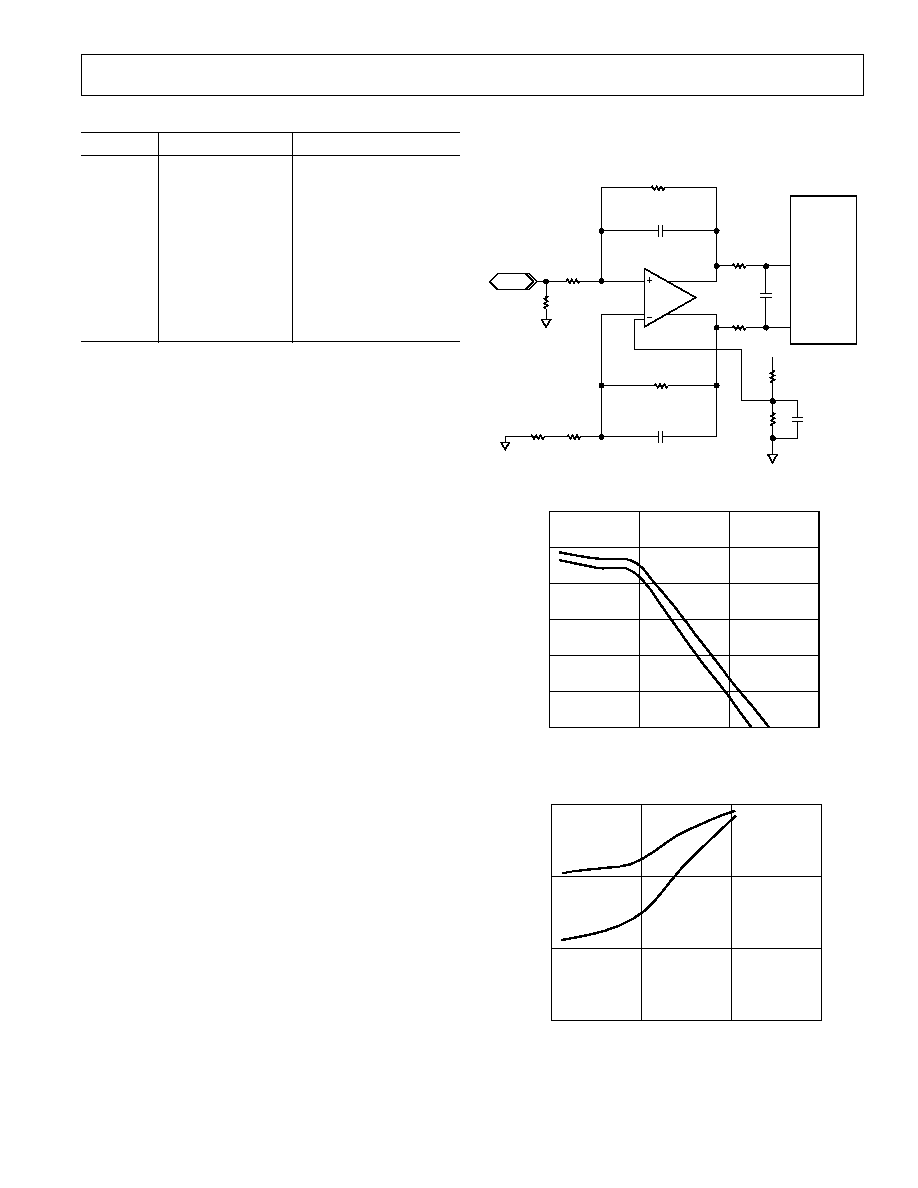
Using the AD8138 to Drive the AD9432
A new differential output op amp from Analog Devices, Inc.,
the AD8138, can be used to drive the AD9432 in dc-coupled
applications. The AD8138 was specifically designed for ADC
driver applications. Superior SNR performance is maintained up
to analog frequencies of 30 MHz. The AD8138 op amp provides
single-ended-to-differential conversion, providing for a low-cost
option to transformer coupling for ac applications as well.
The circuit in Figure 10 was breadboarded and the measured
performance is shown in Figures 11 and 12. The figures shown
are for
±5 V supplies at the AD8138--performance dropped by
about 1 dB2 dB with a single 5 V supply at the AD8138.
Figure 11 shows SNR and SINAD for a 1 dBFS analog input
frequency varied from 2 MHz to 40 MHz with an encode rate of
105 MSPS. The measurements are for nominal conditions at
room temperature. Figure 12 shows the second and third har-
monic distortion performance under the same conditions.
The dc common-mode voltage for the AD8138 outputs can be
adjusted via input V
OCM
to provide the 3 V common-mode voltage
the AD9432 inputs require.
AD8138
500
500
50
50
22pF
AIN
AIN
AD9432
10pF
10pF
500
25
50
500
V
OCM
3k
2k
5V
VIN
0.1 F
Figure 10. AD8138/AD9432 Schematic
AIN MHz
0
dB
20
60
64
40
63
62
61
60
SNR
SINAD
65
66
Figure 11. Measured SNR and SINAD (Encode = 105 MSPS)
AIN MHz
dB
80
90
100
70
H2
H3
0
20
40
60
Figure 12. Measured Second and Third Order Harmonic
Distortion (Encode = 105 MSPS)
REV. E
AD9432
12
EVALUATION BOARD
The AD9432 evaluation board offers an easy way to test the
AD9432. It requires an analog signal, encode clock, and power
supplies as inputs. The clock is buffered on the board to provide
the clocks for an on-board DAC and latches. The digital outputs
and output clock are available at a standard 37-pin connector P7.
Power Connector
Power is supplied to the board via two detachable 4-pin power
strips P30, P40.
P40
P1
VCC2 5 V/165 mA
DAC Supply
P2
GND
P3
VCC
5 V/200 mA
ADC Analog Supply
P4
GND
P30
P5
No Connect
P6
No Connect
P7
VD
3.3 V /105 mA Latch, ADC Digital Output Supply
P8
GND
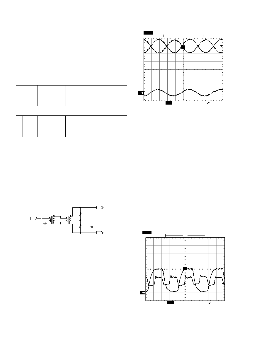
Analog Inputs
The evaluation board accepts a 2 V p-p analog input signal at
SMB connector P2. This single-ended signal is ac-coupled by
capacitor C11 and drives a wideband RF transformer T1 (Mini-
Circuits ADT1-1WT) that converts the single-ended signal to a
differential signal. (The AD9432 should be driven differentially to
provide optimum performance.) The evaluation board is shipped
with termination resistors R4, R5, which provide the effective
50
termination impedance; input termination resistor R10 is
optional. Note: The second harmonic distortion that some RF
transformers tend to introduce at high frequencies can be reduced
by coupling two transformers in series as shown in Figure 13.
(Improvements on the order of 3 dB4 dB can be realized.)
IN
TO AIN+
R1
25
R2
25
C1
0.1 F
TO AIN
T2
T1
C2
0.1 F
Figure 13. Improving Second Harmonic Distortion
Performance
CH2
CH1
CH3
500mV
2.00V
500mV
M 5.00ns CH1
3.00V
STOP:
TEK
5.00GS/s
[T]
14 ACQS
C1 MAX
3.4V
C1 MIN
2.5mV
C1 FREQ
49.995MHz
LOW SIGNAL
AMPLITUDE
T
2
Figure 14. Analog Input Levels
The full-scale analog inputs to the ADC should be two 1 V p-p
signals 180 degrees out of phase with each other, as shown in
Figure 14. The analog inputs are dc biased by two on-chip
resistor dividers that set the common-mode voltage to approxi-
mately 0.6
× VCC (0.6 × 5 = 3 V). AIN+ and AIN each vary
between 2.5 V and 3.5 V as shown in the two upper traces in Fig-
ure 14. The lower trace is the input at SMB P2 (on a 2 V/div scale).
Encode
The encode input to the board is at SMB connector P3. The
(>1 V p-p) input is ac-coupled and drives two high-speed differ-
ential line receivers (MC10EL16). These receivers provide
subnanosecond rise times at their outputs--a requirement for
the ADC clock inputs for optimum performance. The EL16
outputs are PECL levels and must be ac-coupled to meet the
common-mode dc levels required at the AD9432 encode inputs.
A PECL/TTL translator (MC100ELT23), provides the clocks
required at the output latches, DAC, and 37-pin connector.
Note: Jitter performance on the clock source is critical at this
performance level; a stable, crystal-controlled signal generator is
used to generate all of the ADC performance plots. Figure 15
shows the Encode+ clock at the ADC. The 3 V latch clock
generated on the card is also shown in the plot.
[T]
86 ACQS
STOP:
TEK
5.00GS/s
T
2
CH2
CH1
1.00V
1.00V
M 5.00ns
CH1
1.20V
C1 MAX
2.33V
C1 MIN
810mV
C1 FREQ
106.3167MHz
LOW
SIGNAL
AMPLITUDE
Figure 15. Encode+ Clock and Latch Clock
REV. E
AD9432
13
DATA OUTPUTS
The ADC digital outputs are latched on the board by two 574s;
the latch outputs are available at the 37-pin connector at Pins
2536. A latch output clock (data ready) is available at Pin 21,
with the complement at Pin 2. There are series termination
resistors on the data and clock outputs. These can be changed if
required to accommodate different loading situations. Figure
16 shows a data bit switching and output clock (DR) at the
connector.
T
CH2
CH1
1.00V
1.00V
M 5.00ns
CH1
1.20V
2
[T]
265 ACQS
C1 MAX
3.06V
C1 MIN
390mV
C1 FREQ
105.4562MHz
STOP:
TEK
5.00GS/s
Figure 16. Data Bit and Clock at 37-Pin Connector
REFERENCE
The AD9432 has an on-chip reference of 2.5 V available at
VREFOUT (Pin 46). Most applications will simply tie this
output to the VREFIN input (Pin 45). This is accomplished
jumping E4 to E6 on the board. An external voltage reference
can drive the VREFIN pin if desired by strapping E4 to E3 and
placing an AD780 voltage reference on the board (not supplied).
DAC
The evaluation board has an on-board reconstruction DAC
(AD9752). This is placed only to facilitate testing and debug of
the board. It should not be used to measure the performance of
the ADC, as it will not accurately indicate the ADC performance.
The DAC output is available at SMB P1. It will drive a 50
load. Provision to power down the DAC is at Pin 15 at the DAC.
PCB LAYOUT
The PCB is designed on a four-layer (1 oz. Cu) board. Compo-
nents and routing are on the top layer with a ground flood for
additional isolation. Test and ground points were judiciously
placed to facilitate high-speed probing. A common ground plane
exists on the second layer. The third layer has three split power
planes, two for the ADC and one for support logic. The DAC,
components, and routing are located on the bottom layer.
TROUBLESHOOTING
If the board does not seem to be working correctly, try the
following:
· Verify power at IC pins.
· Check that all jumpers are in the correct position for the
desired mode of operation.
· Verify VREF is at 2.5 V.
· Try running encode clock and analog inputs at low speeds
(10 MSPS/1 MHz) and monitor 574 outputs, DAC output,
and ADC outputs for toggling.
The AD9432 Evaluation Board is provided as a design example
for customers of Analog Devices, Inc. ADI makes no warranties,
express, statutory, or implied, regarding merchantability or fitness
for a particular purpose.

REV. E
AD9432
14
PCB Bill of Materials
#
Quantity
REFDES
Device
Package
Value
1
30
C1C8, C10C13, C17, C19C22,
Capacitor
603
0.1
µF
C27C29, C41, C42, C47, C48,
C53, C56, C58, C60, C61, C70
2
1
C9
Capacitor
603
0.01
µF
3
4
C14, C18, C31, C34
Capacitor
CAPTAJD
10
µF
4
1
C15
Capacitor
CAPTAJD
1
µF
5
18
E1E13, E30, E32, E40, E42, E43
E-HOLE
Test Point
6
3
P1, P2, P3
Connector
SMB
7
1
P7
37-Pin Connector
Female
AMP 747462-2
8
2
P30, P40
Power Connector
9
6
R1, R2, R7, R8, R10, R18
Resistor
1206
50
(R1, R2, R10 Optional)
10
2
R3, R35
Resistor
1206
100
11
4
R25, R26, R31, R32
Resistor
1206
500
12
2
R6, R24
Resistor
1206
2 k
13
4
RP1RP4
RES PAK
100
14
1
T1
Transformer
Mini-Circuits
ADT1-1WT
15
1
U1
DAC
SOIC
AD9752
16
1
U2
Reference (Not Supplied)
SOIC
AD780N
17
2
U3, U4
Inverter (U4 Not Supplied)
SC70
NC7SZ04P5
18
1
U9
ADC
52QFP
AD9432
19
2
U12U13
Latch
SOIC
74AC574M
20
1
Z1
PECL/TTL Translator
SOIC
MC100ELT23
21
2
Z2, Z3
Differential Receiver
SOIC
MC10EL16
22
3
R4, R5, R15
Resistor
1206
24.9
REV. E
AD9432
15
10
11
12
13
14
15
16
9
D4
D3
D2
D1
D0
8
7
6
5
4
3
2
1
100
RP2
RPAK
_
742
9
10
11
12
13
14
15
16
8
7
6
5
4
3
2
1
10
11
12
13
14
15
16
9
OR
D11
D10
D9
D8
8
7
6
5
4
3
2
1
100
RPAK
_
742
9
10
11
12
13
14
15
16
8
7
6
5
4
3
2
1
D7
D6
D5
OR
(M
S
B
)
D
1
1
D10
D9
D8
D7
D6
D5
D4
D3
D2
D1
D0
VREFIN
VREFOUT
AIN
AIN
ENC
ENC
AD9432
RP1
14
15
16
17
18
19
20
25
26
27
28
29
30
VCC
52
47
44
37
6
5
2
VD
VCC
13
36
22
23
32
10
9
34
U9
AGND
E1
AGND
C4
0.1
F
42
41
40
39
VCC
FLOAT
AGND
AGND
C2
0.1
F
E4
E5
E3
EXTREF
AGND
E2
VCC
NC
+V
I
N
TEMP
GND
2.5/3V
NC
VOUT
TRIM
U2
(NOT SUPPLIED)
AD780N
C15
1
F
AGND
VCC
1
2
3
4
8
7
6
5
C14
10
F
+
AGND
EXTREF
R10
50
(OPTIONAL)
C11
0.1
F
AGND
T1
ADT1-1WT
6
4
2
1
3
AGND
ANALOG
P2
SMBPN
C9
0.01
F
C70
0.1
F
AGND
AGND
D0
D08
D18
D1
VCC
Q0
Q1
GND
Z1
MC100ELT23
1
2
3
4
8
7
6
5
51
AGND
48
43
38
4
3
1
AGND
AGND
12
35
11
33
21
24
31
C7
0.1
F
C8
0.1
F
AIN
AIN
7
8
50
49
46
45
AGND
VCC2
AGND
C1
0.1
F
AGND
VD
C5
0.1
F
VCC
Y
NC
A
GND
1
2
3
4
5
AGND
NC7SZ04P5
U4 (NOT SUPPLIED)
CLOCK
AGND
VD
R2
100
R1
100
R7
50
R8
50
DR
DR
Z3
MC10EL16
1
2
3
4
8
7
6
5
AGND
VCC2
AGND
C60
0.1
F
AGND
AGND
R25
500
R26
500
AGND
AGND
R31
500
R32
500
AGND
VCC
AGND
C61
0.1
F
NC
D
DB
VBB
VCC
Q
QB
VEE
Z2
MC10EL16
1
2
3
4
8
7
6
5
C58
0.1
F
AGND
NC
D
DB
VBB
VCC
Q
QB
VEE
R4
24.9
R5
24.9
R35
100
C47
0.1
F
ENCODE
P3
SMBPN
C6
0.1
F
AGND
R3
100
PRI SEC
NC = NO CONNECT
(R
1
,
R
2
,
OPTIONAL)
Figure 17a. PCB Schematic
REV. E
AD9432
16
16
15
14
13
12
11
10
9
1
2
3
4
5
6
7
8
100
RP3
16
15
14
13
12
11
10
9
1
2
3
4
5
6
7
8
1
2
3
4
5
6
7
8
9
10
20
19
18
17
16
15
14
13
12
11
AGND
D0
D1
D2
D3
D4
GND
OUT_EN
D0
D1
D2
D3
D4
D5
D6
D7
GND
VCC
Q0
Q1
Q2
Q3
Q4
Q5
Q6
Q7
CLOCK
U13
CLOCK
VD
B0
B1
B2
B3
B4
16
15
14
13
12
11
10
9
1
2
3
4
5
6
7
8
100
RP4
16
15
14
13
12
11
10
9
1
2
3
4
5
6
7
8
1
2
3
4
5
6
7
8
9
10
20
19
18
17
16
15
14
13
12
11
GND
D8
D9
D10
D11
OR
GND
OUT_EN
D0
D1
D2
D3
D4
D5
D6
D7
GND
VCC
Q0
Q1
Q2
Q3
Q4
Q5
Q6
Q7
CLOCK
U12
CLOCK
VD
B5
B6
B7
B8
B9
B10
B11
RPAK_742
RPAK_742
INV
MSB
BOR
D5
D6
D7
74AC574M
74AC574M
37
36
35
34
33
32
31
30
29
28
27
26
25
24
23
22
21
20
19
18
17
16
15
14
13
12
11
10
9
8
7
6
5
4
3
2
AGND
AGND
AGND
AGND
AGND
AGND
AGND
AGND
AGND
AGND
AGND
AGND
AGND
AGND
AGND
AGND
AGND
DR
AGND
1
BOR
B11
B10
B9
B8
B7
B6
B5
B4
B3
B2
B1
B0
DR
P7
P37
P36
P35
P34
P33
P32
P31
P30
P29
P28
P27
P26
P25
P24
P23
P22
P21
P20
P19
P18
P17
P16
P15
P14
P13
P12
P11
P10
P9
P8
P7
P6
P5
P4
P3
P2
P1
AGND
VCC2
C17
0.1
F
CLOCK
GND
AG
N
D
C10
0.1
F
C13
0.1
F
R24
2k
R15
24.9
R18
50
AGND
AGND
P1
SMBPN
C12
0.1
F
AGND
VCC2
DACOUT
AGND
AGND
AGND
VCC2
R6
2k
E1
E8
28
27
26
25
24
23
22
21
20
19
18
17
16
15
1
2
3
4
5
6
7
8
9
10
11
12
13
14
CLK
DVDD
DCON
NC2
AVDD
ICOMP
IOUTA
IOUTB
ACON
NC3
FSADJ
REFIO
REFLO
SLEEP
D11
D10
D9
D8
D7
D6
D5
D4
D3
D2
D1
D0
NC
NC1
U1
AD9752
MSB
B10
B9
B8
B7
B6
B5
B4
B3
B2
B1
B0
AGND
C3
0.1
F
VCC2
5
4
1
2
3
NC
A
GND
VCC
Y
U3
NC7SZ04P5
AGND
INV
E12
E11
E10
E9
E32
E30
AGND
GROUND
PLANE
CONNECTING
E-HOLES
E7
DR
E6
CLOCK
E40
DR
E43
D11
E42
D0
SCOPE
TEST
POINTS
P30
P40
AGND
VD
(+3V)
AGND
VCC
(+5V)
AGND
VCC2
(+5V)
8
7
6
5
4
3
2
1
NC
NC
AGND
C34
10
F
C48
0.1
F
C19
0.1
F
C20
0.1
F
C21
0.1
F
C22
0.1
F
C56
0.1
F
C53
0.1
F
+
VCC
OUT
BYPASS
C18
10
F
AGND
VCC2
C41
0.1
F
C42
0.1
F
AGND
VD
C27
0.1
F
C29
0.1
F
AGND
VD
C28
0.1
F
C31
10
F
+
OUT
BYPASS
LATCHES
AGND
NC = NO CONNECT
Figure 17b. PCB Schematic (Continued)
REV. E
AD9432
17
Figure 18. Top Silkscreen
Figure 19. Top Level Routing
Figure 20. Ground Plane
Figure 21. Split Power Plane
Figure 22. Bottom Layer Route
Figure 23. Bottom Silkscreen
REV. E
AD9432
18
OUTLINE DIMENSIONS
Dimensions shown in inches and (mm).
52-Lead Plastic Quad Flatpack (LQFP)
(ST-52)
TOP VIEW
(PINS DOWN)
40
52
1
14
13
26
27
39
0.026 (0.65)
BSC
0.472 (12.00) SQ
0.394
(10.0)
SQ
0.015 (0.38)
0.009 (0.22)
0.063 (1.60)
MAX
SEATING
PLANE
0.030 (0.75)
0.018 (0.45)
0.006 (0.15)
0.002 (0.05)
0.057 (1.45)
0.053 (1.35)
CONTROLLING DIMENSIONS ARE IN MILLIMETERS; INCH DIMENSIONS
ARE ROUNDED-OFF MILLIMETER EQUIVALENTS FOR REFERENCE
ONLY AND ARE NOT APPROPRIATE FOR USE IN DESIGN
THERMALLY ENHANCED
52-Lead Power Thin Plastic Quad Flatpack (LQFP_ED)
(SQ-52)
0.026 (0.65)
0.015 (0.38)
0.013 (0.32)
0.009 (0.22)
0.472 (12.00) SQ
0.402 (10.20)
0.394 (10.00) SQ
0.386 (9.80)
TOP VIEW
(PINS DOWN)
40
52
1
14
13
26
27
39
0.307 (7.80)
0.063
(1.60)
MAX
VIEW A
SEATING
PLANE
0.030 (0.75)
0.024 (0.60)
0.018 (0.45)
0.006 (0.15)
0.002 (0.05)
VIEW A
0.004 (0.10)
COPLANARITY
0.057 (1.45)
0.055 (1.40)
0.053 (1.35)
40
52
1
14
13
26
27
39
EXPOSED
HEATSINK
(CENTERED)
0.093 (2.35)
0.087 (2.20)
0.081 (2.05)
(4 PLCS)
0.236 (6.00)
0.232 (5.90)
0.228 (5.80)
0.236 (6.00)
0.232 (5.90)
0.228 (5.80)
0.104 (2.65)
0.098 (2.50)
0.093 (2.35)
(4 PLCS)
BOTTOM VIEW
(PINS UP)
NOTES
1. CONTROLLING DIMENSIONS ARE IN MILLIMETERS; INCH DIMENSIONS ARE ROUNDED-OFF MILLIMETER
EQUIVALENTS FOR REFERENCE ONLY AND ARE NOT APPROPRIATE FOR USE IN DESIGN.
2. ALTHOUGH NOT REQUIRED IN ALL APPLICATIONS, THE AD9432 HAS AN EXPOSED METALLIC PAD ON THE
PACKAGE BOTTOM WHICH IS INTENDED TO ENHANCE THE HEAT REMOVAL PATH. TO MAXIMIZE THE REMOVAL
OF HEAT, A LAND PATTERN WITH CLOSELY SPACED THERMAL VIAS TO THE GROUND PLANE(S) SHOULD
BE INCORPORATED ON THE PCB WITHIN THE FOOTPRINT OF THE PACKAGE CORRESPONDING TO THE
EXPOSED METAL PAD DIMENSIONS OF THE PACKAGE. THE SOLDERABLE LAND AREA SHOULD BE SOLDER
MASK DEFINED AND BE AT LEAST THE SAME SIZE AND SHAPE AS THE EXPOSED PAD AREA ON THE
PACKAGE. AT LEAST 0.25 MM CLEARANCE BETWEEN THE OUTER EDGES OF THE LAND PATTERN AND THE
INNER EDGES OF THE PAD PATTERN SHOULD BE MAINTAINED TO AVOID ANY SHORTS.

REV. E
AD9432
19
Revision History
Location
Page
Data Sheet changed from REV. D to REV. E.
Edits to SPECIFICATIONS . . . . . . . . . . . . . . . . . . . . . . . . . . . . . . . . . . . . . . . . . . . . . . . . . . . . . . . . . . . . . . . . . . . . . . . . . . . . . . . 3
Edits to ABSOLUTE MAXIMUM RATINGS . . . . . . . . . . . . . . . . . . . . . . . . . . . . . . . . . . . . . . . . . . . . . . . . . . . . . . . . . . . . . . . . . 3
Edits to ORDERING GUIDE . . . . . . . . . . . . . . . . . . . . . . . . . . . . . . . . . . . . . . . . . . . . . . . . . . . . . . . . . . . . . . . . . . . . . . . . . . . . . . 3
Addition of text to USING THE AD9432 section . . . . . . . . . . . . . . . . . . . . . . . . . . . . . . . . . . . . . . . . . . . . . . . . . . . . . . . . . . . . . . . 9
Edits to Figure 17a . . . . . . . . . . . . . . . . . . . . . . . . . . . . . . . . . . . . . . . . . . . . . . . . . . . . . . . . . . . . . . . . . . . . . . . . . . . . . . . . . . . . . 13
Edits to Figure 17b . . . . . . . . . . . . . . . . . . . . . . . . . . . . . . . . . . . . . . . . . . . . . . . . . . . . . . . . . . . . . . . . . . . . . . . . . . . . . . . . . . . . . 14
Addition of SQ-52 Package Outline . . . . . . . . . . . . . . . . . . . . . . . . . . . . . . . . . . . . . . . . . . . . . . . . . . . . . . . . . . . . . . . . . . . . . . . . . 16

20
C0058701/02(E)
PRINTED IN U.S.A.