/home/web/htmldatasheet/RUSSIAN/html/ad/164431
REV. 0
Information furnished by Analog Devices is believed to be accurate and
reliable. However, no responsibility is assumed by Analog Devices for its
use, nor for any infringements of patents or other rights of third parties
which may result from its use. No license is granted by implication or
otherwise under any patent or patent rights of Analog Devices.
a
AD9410
One Technology Way, P.O. Box 9106, Norwood, MA 02062-9106, U.S.A.
Tel: 781/329-4700
World Wide Web Site: http://www.analog.com
Fax: 781/326-8703
© Analog Devices, Inc., 2000
10-Bit, 210 MSPS
A/D Converter
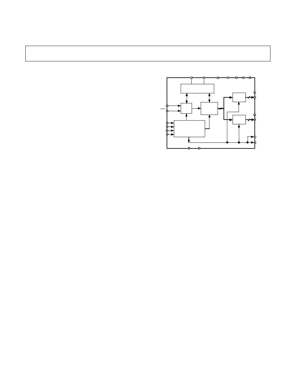
FUNCTIONAL BLOCK DIAGRAM
T/H
A
IN
A
IN
DS
ENCODE
DS
ENCODE
ADC
10-BIT
CORE
TIMING AND
SYNCHRONIZATION
PORT
A
DFS
I/P
REF
IN
REF
OUT
REFERENCE
V
DD
DGND V
D
AGND
V
CC
OR
A
D9
A
D0
A
DCO
OR
B
D9
B
D0
B
10
DCO
AD9410
10
PORT
B
10
FEATURES
SNR = 54 dB with 99 MHz Analog Input
500 MHz Analog Bandwidth
On-Chip Reference and Track/Hold
1.5 V p-p Differential Analog Input Range
5.0 V and 3.3 V Supply Operation
3.3 V CMOS/TTL Outputs
Power: 2.1 W Typical at 210 MSPS
Demultiplexed Outputs Each at 105 MSPS
Output Data Format Option
Data Sync Input and Data Clock Output Provided
Interleaved or Parallel Data Output Option
APPLICATIONS
Communications and Radar
Local Multipoint Distribution Service (LMDS)
High-End Imaging Systems and Projectors
Cable Reverse Path
Point-to-Point Radio Link
GENERAL DESCRIPTION
The AD9410 is a 10-bit monolithic sampling analog-to-digital
converter with an on-chip track-and-hold circuit and is opti-
mized for high-speed conversion and ease of use. The product
operates at a 210 MSPS conversion rate, with outstanding
dynamic performance over its full operating range.
The ADC requires a 5.0 V and 3.3 V power supply and up to a
210 MHz differential clock input for full performance operation.
No external reference or driver components are required for many
applications. The digital outputs are TTL/CMOS-compatible,
and separate output power supply pins also support interfacing
with 3.3 V logic.
The clock input is differential and TTL/CMOS-compatible. The
10-bit digital outputs can be operated from 3.3 V (2.5 V to 3.6 V)
supplies. Two output buses support demultiplexed data up to
105 MSPS rates, and binary or two's complement output coding
format is available. A data sync function is provided for timing-
dependent applications. An output clock simplifies interfacing to
external logic. The output data bus timing is selectable for parallel
or interleaved mode, allowing for flexibility in latching output data.
Fabricated on an advanced BiCMOS process, the AD9410
is available in an 80-lead surface-mount plastic package
(PowerQuad
®
2) specified over the industrial temperature range
(40
°C to +85°C).
PowerQuad is a registered trademark of Amkor Electronics, Inc.
PRODUCT HIGHLIGHTS
High Resolution at High Speed--The architecture is specifically
designed to support conversion up to 210 MSPS with outstand-
ing dynamic performance.
Demultiplexed Output--Output data is decimated by two and
provided on two data ports for ease of data transport.
Output Data Clock--The AD9410 provides an output data
clock synchronous with the output data, simplifying the timing
between data and other logic.
Data Synchronization--A DS input is provided to allow for
synchronization of two or more AD9410s in a system, or
to synchronize data to a specific output port in a single
AD9410 system.

REV. 0
2
AD9410SPECIFICATIONS
DC SPECIFICATIONS
Test
Parameter
Temp
Level
Min
Typ
Max
Unit
RESOLUTION
10
Bits
DC ACCURACY
No Missing Codes
1
Full
IV
Guaranteed
Differential Nonlinearity
25
°C
I
1.0
±0.5
+1.25
LSB
Full
VI
1.0
+1.5
LSB
Integral Nonlinearity
25
°C
I
2.5
±1.65
+2.5
LSB
Full
VI
3.0
+3.0
LSB
Gain Error
25
°C
I
6.0
0
+6.0
% FS
Gain Tempco
Full
V
130
ppm/
°C
ANALOG INPUT
Input Voltage Range (With Respect to
AIN)
Full
V
±768
mV p-p
Common-Mode Voltage
Full
V
3.0
V
Input Offset Voltage
25
°C
I
15
+3
+15
mV
Full
VI
20
+20
mV
Reference Voltage
Full
VI
2.4
2.5
2.6
V
Reference Tempco
Full
V
50
ppm/
°C
Input Resistance
Full
VI
610
875
1250
Input Capacitance
25
°C
V
3
pF
Analog Bandwidth, Full Power
25
°C
V
500
MHz
POWER SUPPLY
Power Dissipation AC
2
25
°C
V
2.1
W
Power Dissipation DC
3
Full
VI
2.0
2.4
W
I
VCC
3
Full
VI
128
145
mA
I
VD
3
Full
VI
401
480
mA
Power Supply Rejection Ratio PSRR
25
°C
I
7.5
+0.5
+7.5
mV/V
NOTES
1
Package heat slug should be attached when operating at greater than 70
°C ambient temperature.
2
Encode = 210 MSPS, A
IN
= 0.5 dBFS 10 MHz sine wave, I
VDD
= 31 mA typical at C
LOAD
= 5 pF.
3
Encode = 210 MSPS, A
IN
= dc, outputs not switching.
Specifications subject to change without notice.
SWITCHING SPECIFICATIONS
Test
Parameter
Temp
Level
Min
Typ
Max
Unit
SWITCHING PERFORMANCE
Maximum Conversion Rate
Full
VI
210
MSPS
Minimum Conversion Rate
Full
IV
100
MSPS
Encode Pulsewidth High (t
EH
)
25
°C
IV
1.2
2.4
ns
Encode Pulsewidth Low (t
EL
)
25
°C
IV
1.2
2.4
ns
Aperture Delay (t
A
)
25
°C
V
1.0
ns
Aperture Uncertainty (Jitter)
25
°C
V
0.65
ps rms
Output Valid Time (t
V
)
Full
VI
3.0
ns
Output Propagation Delay (t
PD
)
Full
VI
7.4
ns
Output Rise Time (t
R
)
25
°C
V
1.8
ns
Output Fall Time (t
F
)
25
°C
V
1.4
ns
CLKOUT Propagation Delay
1
(t
CPD
)
Full
VI
2.6
4.8
6.4
ns
Data to DCO Skew (t
PD
t
CPD
)
Full
IV
0
1
2
ns
DS Setup Time (t
SDS
)
Full
IV
0.5
ns
DS Hold Time (t
HDS
)
Full
IV
0
ns
Interleaved Mode (A, B Latency)
Full
VI
A = 6, B = 6
Cycles
Parallel Mode (A, B Latency)
Full
VI
A = 7, B = 6
Cycles
NOTES
1
C
LOAD
= 5 pF.
Specifications subject to change without notice.
(V
DD
= 3.3 V, V
D
= 3.3 V, V
CC
= 5.0 V; 2.5 V external reference; A
IN
= 0.5 dBFS; Clock
input = 210 MSPS; T
A
= 25 C; unless otherwise noted.)
(V
DD
= 3.3 V, V
D
= 3.3 V, V
CC
= 5.0 V; 2.5 V external reference; A
IN
= 0.5 dBFS; Clock input = 210 MSPS;
T
A
= 25 C; unless otherwise noted.)

REV. 0
3
AD9410
DIGITAL SPECIFICATIONS
Test
Parameter
Temp
Level
Min
Typ
Max
Unit
DIGITAL INPUTS
DFS, Input Logic "1" Voltage
Full
IV
4
V
DFS, Input Logic "0" Voltage
Full
IV
1
V
DFS, Input Logic "1" Current
Full
V
50
µA
DFS, Input Logic "0" Current
Full
V
50
µA
I/P Input Logic "1" Current
1
Full
V
400
µA
I/P Input Logic "0" Current
1
Full
V
1
µA
ENCODE,
ENCODE Differential Input Voltage
Full
IV
0.4
V
ENCODE,
ENCODE Differential Input Resistance
Full
V
1.6
k
ENCODE,
ENCODE Common-Mode Input Voltage
2
Full
V
1.5
V
DS,
DS Differential Input Voltage
Full
IV
0.4
V
DS,
DS Common-Mode Input Voltage
Full
V
1.5
V
Digital Input Pin Capacitance
25
°C
V
3
pF
DIGITAL OUTPUTS
Logic "1" Voltage (V
DD
= 3.3 V)
Full
VI
V
DD
0.05
V
Logic "0" Voltage (V
DD
= 3.3 V)
Full
VI
0.05
V
Output Coding
Binary or Two's Complement
NOTES
1
I/P pin Logic "1" = 5 V, Logic "0" = GND. It is recommended to place a series 2.5 k
(±10%) resistor to V
DD
when setting to Logic "1" to limit input current.
2
See Encode Input section in Applications section.
Specifications subject to change without notice.
AC SPECIFICATIONS
Test
Parameter
Temp
Level
Min
Typ
Max
Unit
DYNAMIC PERFORMANCE
Transient Response
25
°C
V
2
ns
Overvoltage Recovery Time
25
°C
V
2
ns
Signal-to-Noise Ratio (SNR)
(Without Harmonics)
f
IN
= 10.3 MHz
25
°C
I
52.5
55
dB
f
IN
= 82 MHz
25
°C
I
52
54
dB
f
IN
= 160 MHz
25
°C
V
53
dB
Signal-to-Noise Ratio (SINAD)
(With Harmonics)
f
IN
= 10.3 MHz
25
°C
I
51
54
dB
f
IN
= 82 MHz
25
°C
I
50
53
dB
f
IN
= 160 MHz
25
°C
V
52
dB
Effective Number of Bits
f
IN
= 10.3 MHz
25
°C
I
8.3
8.8
Bits
f
IN
= 82 MHz
25
°C
I
8.1
8.6
Bits
f
IN
= 160 MHz
25
°C
V
8.4
Bits
Second Harmonic Distortion
f
IN
= 10.3 MHz
25
°C
I
56
65
dBc
f
IN
= 82 MHz
25
°C
I
55
63
dBc
f
IN
= 160 MHz
25
°C
V
65
dBc
Third Harmonic Distortion
f
IN
= 10.3 MHz
25
°C
I
58
69
dBc
f
IN
= 82 MHz
25
°C
I
57
67
dBc
f
IN
= 160 MHz
25
°C
V
62
dBc
Spurious Free Dynamic Range (SFDR)
f
IN
= 10.3 MHz
25
°C
I
56
61
dBc
f
IN
= 82 MHz
25
°C
I
54
60
dBc
f
IN
= 160 MHz
25
°C
V
58
dBc
Two-Tone Intermod Distortion IMD
1
f
IN1
= 80.3 MHz, f
IN2
= 81.3 MHz
25
°C
V
58
dBFS
NOTES
1
IN1, IN2 level = 7 dBFS.
Specifications subject to change without notice.
(V
DD
= 3.3 V, V
D
= 3.3 V, V
CC
= 5.0 V; 2.5 V external reference; A
IN
= 0.5 dBFS;
Clock input = 210 MSPS; T
A
= 25 C; unless otherwise noted.)
(V
DD
= 3.3 V, V
D
= 3.3 V, V
CC
= 5.0 V; 2.5 V external reference; A
IN
= 0.5 dBFS; Clock input = 210 MSPS;
T
A
= 25 C; unless otherwise noted.)
REV. 0
AD9410
4
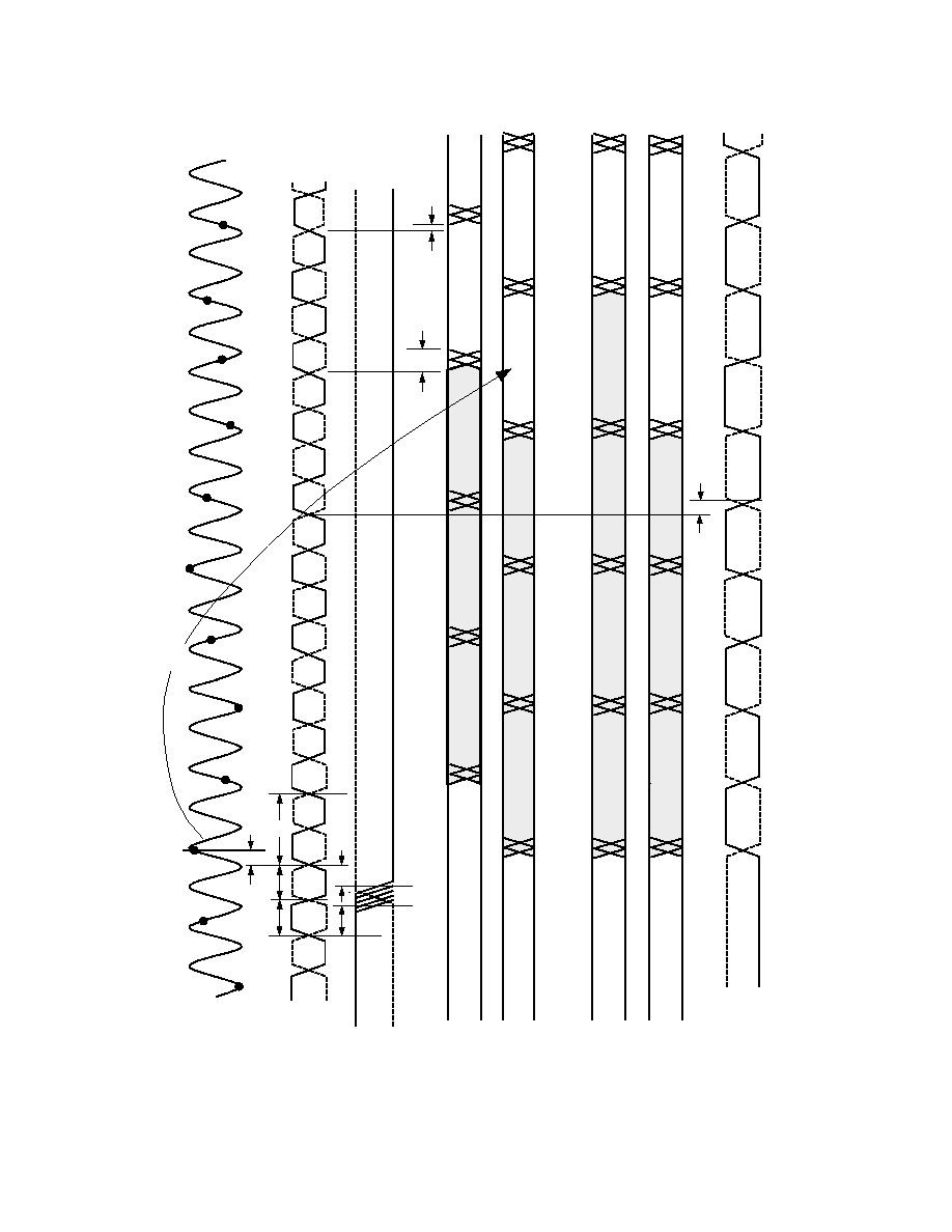
AIN
ENCODE
ENCODE
DS
DS
PORT A
D7
D0
PORT B
D7
D0
PORT A
D7
D0
PORT B
D7
D0
DCO
DCO
SAMPLE N
1
SAMPLE N
SAMPLE N+4
SAMPLE N+5
SAMPLE N+3
t
EL
t
EH
1/f
S
t
A
t
SDS
t
HDS
SAMPLE N
2
SAMPLE N+1
SAMPLE N+2
SAMPLE N+6
INTERLEAVED DATA OUT
INVALID
t
V
t
PD
STATIC
INVALID
INVALID
INVALID
INVALID
INVALID
DATA N
DATA N+2
DATA N+3
DATA N+1
STATIC
PARALLEL DATA OUT
t
CPD
DATA N+1
DATA N
DATA N+2
INVALID
INVALID
INVALID
INVALID
INVALID
INVALID
INVALID
STATIC
STATIC
STATIC
Figure 1. Timing Diagram

REV. 0
AD9410
5
ORDERING GUIDE
Temperature
Package
Package
Model
Range
Description
Option
AD9410BSQ
40
°C to +85°C
PowerQuad 2
SQ-80
AD9410/PCB
25
°C
Evaluation Board
CAUTION
ESD (electrostatic discharge) sensitive device. Electrostatic charges as high as 4000 V readily
accumulate on the human body and test equipment and can discharge without detection. Although
the AD9410 features proprietary ESD protection circuitry, permanent damage may occur on
devices subjected to high-energy electrostatic discharges. Therefore, proper ESD precautions are
recommended to avoid performance degradation or loss of functionality.
WARNING!
ESD SENSITIVE DEVICE
EXPLANATION OF TEST LEVELS
Test Level
I.
100% production tested.
II.
100% production tested at 25
°C and sample tested at
specified temperatures.
III. Sample tested only.
IV. Parameter is guaranteed by design and characterization
testing.
V.
Parameter is a typical value only.
VI. 100% production tested at 25
°C; guaranteed by design and
characterization testing for industrial temperature range.
ABSOLUTE MAXIMUM RATINGS
1
V
D
, V
CC,
V
DD
. . . . . . . . . . . . . . . . . . . . . . . . . . . . . . . . . . . 6 V
Analog Inputs . . . . . . . . . . . . . . . . . . . . . 0 V to V
CC
+ 0.5 V
Digital Inputs . . . . . . . . . . . . . . . . . . . . . 0 V to V
DD
+ 0.5 V
VREF IN . . . . . . . . . . . . . . . . . . . . . . . . . . 0 V to V
D
+ 0.5 V
Digital Output Current . . . . . . . . . . . . . . . . . . . . . . . . 20 mA
Operating Temperature . . . . . . . . . . . . . . . . 55
°C to +125°C
Storage Temperature . . . . . . . . . . . . . . . . . . 65
°C to +150°C
Maximum Junction Temperature
2
. . . . . . . . . . . . . . . . 150
°C
NOTES
1
Absolute maximum ratings are limiting values to be applied individually, and
beyond which the serviceability of the circuit may be impaired. Functional
operability is not necessarily implied. Exposure to absolute maximum rating
conditions for an extended period of time may affect device reliability. Stresses
above those listed under Absolute Maximum Ratings may cause permanent
damage to the device. This is a stress rating only; functional operation of the device
at these or any other conditions outside of those indicated in the operation sections
of this specification is not implied.
2
Typical
JA
= 22
°C/W (heat slug not soldered), typical
JA
= 16
°C/W (heat slug
soldered), for multilayer board in still air with solid ground plane.

REV. 0
AD9410
6
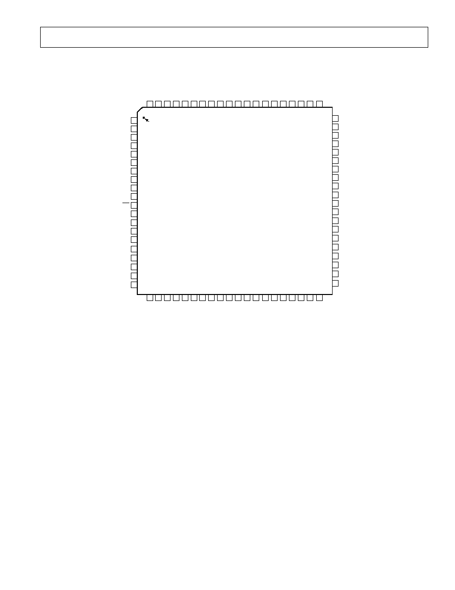
PIN FUNCTION DESCRIPTIONS
Pin No.
Mnemonic
Function
1, 2, 8, 9, 12, 13, 16, 17, 20, 21, 24,
AGND
Analog Ground.
27, 28, 29, 30, 71, 72, 73, 74, 77, 78
3, 7, 14, 15
V
CC
5 V Supply. (Regulate to within
±5%.)
4
REF
OUT
Internal Reference Output.
5
REF
IN
Internal Reference Input.
6
DNC
Do Not Connect.
10
A
IN
Analog Input--True.
11
AIN
Analog Input--Complement.
18
ENCODE
Clock Input--True.
19
ENCODE
Clock Input--Complement.
22
DS
Data Sync (Input)--True. Tie LOW if not used.
23
DS
Data Sync (Input)--Complement. Float and decouple with 0.1
µF
capacitor if not used.
25, 26, 31, 32, 69, 70, 75, 76
V
D
3.3 V Analog Supply. (Regulate to within
±5%.)
33, 40, 49, 52, 59, 68
DGND
Digital Ground.
34, 41, 48, 53, 60, 67
V
DD
3.3 V Digital Output Supply. (2.5 V to 3.6 V)
3539
D
B0
D
B4
Digital Data Output for Channel B. (LSB = D
B0
.)
4246
D
B5
D
B9
Digital Data Output for Channel B. (MSB = D
B9
.)
47
OR
B
Data Overrange for Channel B.
50
DCO
Clock Output--Complement.
51
DCO
Clock Output--True.
5458
D
A0
D
A4
Digital Data Output for Channel A. (LSB = D
A0
.)
6165
D
A5
D
A9
Digital Data Output for Channel A. (MSB = D
A9
.)
66
OR
A
Data Overrange for Channel A.
79
DFS
Data Format Select. HIGH = Two's Complement, LOW = Binary.
80
I/P
Interleaved or Parallel Output Mode. Low = Parallel Mode, High =
Interleaved Mode. If tying high, use a current limiting series resistor
(2.5 k
) to the 5 V supply.
REV. 0
AD9410
7
PIN CONFIGURATION
PIN 1
IDENTIFIER
TOP VIEW
80-Lead PowerQuad2
(Not to Scale)
AD9410
60
59
58
57
56
55
54
53
52
51
50
49
48
47
46
45
44
43
42
41
20
19
18
17
16
15
14
13
12
11
10
9
8
7
6
5
4
3
2
1
80
79
78
77
76
75
74
73
72
71
70
69
68
67
66
65
64
63
62
61
21
22
23
24
25
26
27
28
29
30
31
32
33
34
35
36
37
38
39
40
AGND
AGND
V
CC
REF
OUT
REF
IN
DNC
V
CC
AGND
AGND
A
IN
A
IN
AGND
AGND
V
CC
V
CC
AGND
AGND
ENCODE
ENCODE
AGND
AGND
DS
DS
AGND
V
D
V
D
AGND
AGND
AGND
AGND
V
D
V
D
DGND
V
DD
(LSB) D
B0
D
B1
D
B2
D
B3
D
B4
DGND
V
DD
D
B5
D
B6
D
B7
D
B8
D
B9
(MSB)
OR
B
V
DD
DGND
DCO
DCO
DGND
V
DD
D
A0
(LSB)
D
A1
D
A2
D
A3
D
A4
DGND
V
DD
D
A5
D
A6
D
A7
D
A8
D
A9
(MSB)
OR
A
V
DD
DGND
V
D
V
D
AGND
AGND
AGND
AGND
V
D
V
D
AGND
AGND
DFS
I/P
DNC
DO NOT CONNECT

REV. 0
AD9410
8
DEFINITIONS OF SPECIFICATIONS
Analog Bandwidth
The analog input frequency at which the spectral power of the
fundamental frequency (as determined by the FFT analysis) is
reduced by 3 dB.
Aperture Delay
The delay between the 50% point of the rising edge of the
ENCODE command and the instant at which the analog
input is sampled.
Aperture Uncertainty (Jitter)
The sample-to-sample variation in aperture delay.
Differential Analog Input Resistance, Differential Analog
Input Capacitance, and Differential Analog Input Impedance
The real and complex impedances measured at each analog
input port. The resistance is measured statically and the capaci-
tance and differential input impedances are measured with a
network analyzer.
Differential Analog Input Voltage Range
The peak-to-peak differential voltage that must be applied to the
converter to generate a full-scale response. Peak differential voltage
is computed by observing the voltage on a single pin and subtract-
ing the voltage from the other pin, which is 180 degrees out of
phase. Peak-to-peak differential is computed by rotating the
inputs phase 180 degrees and taking the peak measurement
again. The difference is then computed between both peak
measurements.
Differential Nonlinearity
The deviation of any code width from an ideal 1 LSB step.
Effective Number of Bits
The effective number of bits (ENOB) is calculated from the
measured SINAD based on the equation.
ENOB
SINAD
dB
Full Scale Amplitude
Input Amplitude
MEASURED
=
+
.
log
.
1 76
20
6 02
Encode Pulsewidth/Duty Cycle
Pulsewidth high is the minimum amount of time that the
ENCODE pulse should be left in Logic 1 state to achieve
rated performance; pulsewidth low is the minimum time
ENCODE pulse should be left in low state. See timing implica-
tions of changing t
ENCH
in text. At a given clock rate, these specs
define an acceptable ENCODE duty cycle.
Full-Scale Input Power
Expressed in dBm. Computed using the following equation:
POWER
V
Z
FULL SCALE
FULL SCALE
INPUT
rms
=
10
0 001
2
log
.
Harmonic Distortion, Second
The ratio of the rms signal amplitude to the rms value of the
second harmonic component, reported in dBc.
Harmonic Distortion, Third
The ratio of the rms signal amplitude to the rms value of the
third harmonic component, reported in dBc.
Integral Nonlinearity
The deviation of the transfer function from a reference line
measured in fractions of 1 LSB using a "best straight line"
determined by a least-square curve fit.
Minimum Conversion Rate
The encode rate at which the SNR of the lowest analog
signal frequency drops by no more than 3 dB below the
guaranteed limit.
Maximum Conversion Rate
The encode rate at which parametric testing is performed.
Output Propagation Delay
The delay between a differential crossing of ENCODE and
ENCODE and the time when all output data bits are within
valid logic levels.
Out-of-Range Recovery Time
Out-of-range recovery time is the time it takes for the ADC to
reacquire the analog input after a transient from 10% above
positive full scale to 10% above negative full scale, or from 10%
below negative full scale to 10% below positive full scale.
Noise (For Any Range Within the ADC)
V
Z
NOISE
FS
SIGNAL
dBm
dBFS
=
×
×
-
| |
.
0 001 10
10
Where Z is the input impedance, FS is the full scale of the device
for the frequency in question, SNR is the value for the particular
input level, and SIGNAL is the signal level within the ADC
reported in dB below full scale. This value includes both thermal
and quantization noise.
Power Supply Rejection Ratio
The ratio of a change in input offset voltage to a change in
power supply voltage.
Signal-to-Noise-and-Distortion (SINAD)
The ratio of the rms signal amplitude (set 0.5 dB below full
scale) to the rms value of the sum of all other spectral compo-
nents, including harmonics, but excluding dc.
Signal-to-Noise Ratio (Without Harmonics)
The ratio of the rms signal amplitude (set at 0.5 dB below full
scale) to the rms value of the sum of all other spectral compo-
nents, excluding the first five harmonics and dc.
Spurious-Free Dynamic Range (SFDR)
The ratio of the rms signal amplitude to the rms value of the
peak spurious spectral component. The peak spurious compo-
nent may or may not be a harmonic. May be reported in dBc
(i.e., degrades as signal level is lowered), or dBFS (always
related back to converter full scale).
Transient Response Time
Transient response time is defined as the time it takes for the
ADC to reacquire the analog input after a transient from 10%
above negative full scale to 10% below positive full scale.
Two-Tone Intermodulation Distortion Rejection
The ratio of the rms value of either input tone to the rms value
of the worst third order intermodulation product; reported in dBc.
Two-Tone SFDR
The ratio of the rms value of either input tone to the rms value
of the peak spurious component. The peak spurious component
may or may not be an IMD product. May be reported in dBc
(i.e., degrades as signal level is lowered), or in dBFS (always
related back to converter full scale).
Worst Other Spur
The ratio of the rms signal amplitude to the rms value of the
worst spurious component (excluding the second and third
harmonic) reported in dBc.
REV. 0
AD9410
9
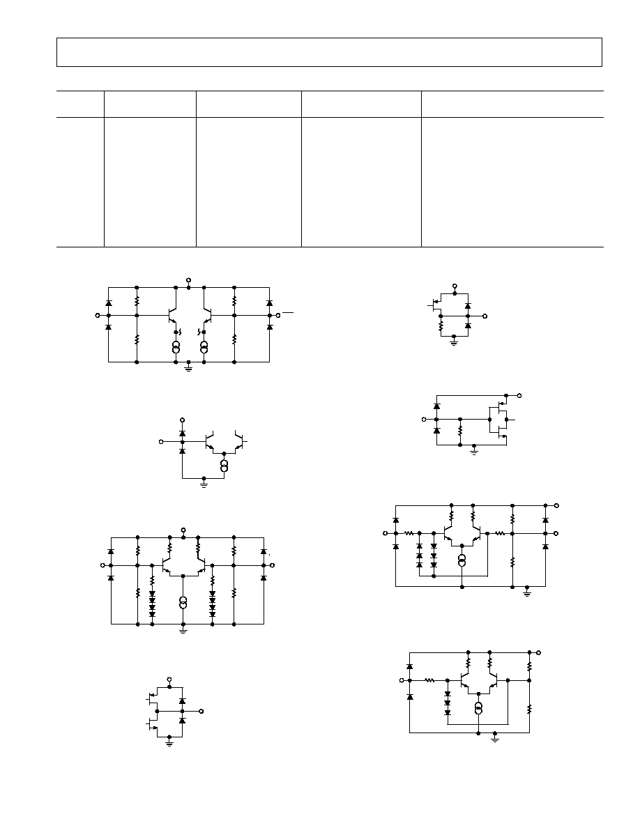
V
CC
1.5k
A
IN
2.25k
1.5k
2.25k
A
IN
Figure 2. Equivalent Analog Input Circuit
V
CC
VREFIN
Figure 3. Equivalent Reference Input Circuit
17k
V
CC
17k
8k
8k
ENCODE
100
100
ENCODE
450
450
Figure 4 Equivalent Encode Input Circuit
V
DD
DIGITAL
OUTPUT
Figure 5. Equivalent Digital Output Circuit
Table I. Output Coding (V
REF
= 2.5 V)
Digital Outputs
Digital Outputs
Step
A
IN
A
IN
Offset Binary
Two's Complement
OR
A
, OR
B
> 0.768
11 1111 1111
01 1111 1111
1
1023
0.768
11 1111 1111
01 1111 1111
0
·
·
·
·
·
·
·
·
·
·
513
0.0015
10 0000 0001
00 0000 0001
0
512
0.0
10 0000 0000
00 0000 0000
0
511
0.0015
01 1111 1111
11 1111 1111
0
·
·
·
·
·
·
·
·
·
·
0
0.768
00 0000 0000
10 0000 0000
0
< 0.768
00 0000 0000
10 0000 0000
1
V
CC
VREFOUT
Figure 6. Equivalent Reference Output Circuit
100k
DFS
V
CC
Figure 7. Equivalent DFS Input Circuit
7.5k
DS
300
17.5k
300
DS
V
CC
Figure 8. Equivalent DS Input Circuit
7.5k
I/P
300
17.5k
V
CC
Figure 9. Equivalent I/P Input Circuit
REV. 0
AD9410
10
MHz
0
0
dB
20
40
60
80
100
120
105
ENCODE = 210MSPS
A
IN
= 40MHz @ 0.5dBFS
SNR = 54.5dB
SINAD = 53.5dB
TPC 1. Single Tone at 40 MHz, Encode = 210 MSPS
MHz
0
0
dB
20
40
60
80
100
120
105
ENCODE = 210MSPS
A
IN
= 100MHz @ 0.5dBFS
SNR = 53.5dB
SINAD = 52.5dB
TPC 2. Single Tone at 100 MHz, Encode = 210 MSPS
MHz
0
0
dB
20
40
60
80
100
120
105
ENCODE = 210MSPS
A
IN
= 160MHz @ 0.5dBFS
SNR = 53dB
SINAD = 52dB
TPC 3. Single Tone at 160 MHz, Encode = 210 MSPS
Typical Performance Characteristics
A
IN
MHz
51
0
dB
50
49
48
47
46
45
50
100
150
200
250
53
55
SNR
SINAD
52
54
TPC 4. SNR/SINAD vs. A
IN
Encode = 210 MSPS
MHz
53.0
100
dB 52.5
52.0
51.5
51.0
50.5
50.0
120
140
160
200
240
54.0
55.0
SNR
SINAD
53.5
54.5
180
220
TPC 5. SNR/SINAD vs. F
S
A
IN
= 70 MHz
ns
40
0
dB
35
30
0.5
1.0
1.5
2.5
4.0
55
60
50
2.0
3.5
45
3.0
SINAD
SNR
TPC 6. SNR/SINAD vs. Encode Positive Pulsewidth
(F
S
= 210 MSPS, A
IN
= 70 MHz)
REV. 0
AD9410
11
MHz
0
0
dB
20
40
60
80
100
120
105
ENCODE = 210MSPS
A
IN
1, A
IN
2 = 7dBFS
SFDR = 62dBFS
TPC 7. Two Tone Test A
IN
1 = 80.3 MHz, A
IN
2 = 81.3 MHz
TEMPERATURE C
54.5
40
dB
54.0
53.5
53.0
52.5
52.0
51.5
20
0
20
40
60
80
100
120
55.0
55.5
SNR
SINAD
TPC 8. SNR/SINAD vs. Temperature,
Encode = 210 MSPS, A
IN
= 70 MHz
TEMPERATURE C
70
40
dB
68
66
64
62
60
58
20
0
20
40
60
80
100
120
72
74
H2
H3
TPC 9. Second and Third Harmonics vs. Temperature;
A
IN
= 70 MHz, Encode = 210 MSPS
ANALOG SUPPLY
2.48
4.0
VOLTS
2.47
2.46
4.2
4.4
4.6
5.0
5.6
2.51
2.52
2.50
4.8
5.4
2.49
5.2
TPC 10. VREF
OUT
vs. Analog 5 V Supply
MSPS
110
100
mA
60
10
120
140
160
200
260
310
210
180
160
220
360
410
460
IAhi3
IAhi5
Ivdd
TPC 11. Power Supply Currents vs. Encode
mA
2.35
0
VOLTS
2.30
2.25
0.5
1.0
2.0
1.5
2.40
2.5
2.45
2.50
2.55
TPC 12. VREF
OUT
vs. I
LOAD
REV. 0
AD9410
12
TEMPERATURE C
40
VOLTS
20
0
40
20
60
2.503
2.502
2.501
2.500
2.499
2.498
2.497
2.496
80
TPC 13. VREF
OUT
vs. Temperature
TEMPERATURE C
40
ns
20
0
40
20
60
5.1
4.9
4.7
4.5
4.3
4.1
3.9
80
T
PD
T
V
T
CPD
TPC 14. T
PD
, T
V
, T
CPD
vs. Temperature
REV. 0
AD9410
13
APPLICATION NOTES
THEORY OF OPERATION
The AD9410 architecture is optimized for high speed and ease
of use. The analog inputs drive an integrated high bandwidth
track-and-hold circuit that samples the signal prior to quantiza-
tion by the flash 10-bit core. For ease of use the part includes
an onboard reference and input logic that accepts TTL, CMOS,
or PECL levels.
USING THE AD9410
ENCODE Input
Any high-speed A/D converter is extremely sensitive to the
quality of the sampling clock provided by the user. A Track/Hold
circuit is essentially a mixer, and any noise, distortion, or timing
jitter on the clock will be combined with the desired signal at the
A/D output. For that reason, considerable care has been taken
in the design of the ENCODE input of the AD9410, and the
user is advised to give commensurate thought to the clock source.
To limit SNR degradation to less than 1 dB, a clock source with
less than 1.25 ps rms jitter is required for sampling at Nyquist.
(Valpey Fisher VF561 is an example.) Note that required jitter
accuracy is a function of input frequency and amplitude. Consult
Analog Devices' application note AN-501, "Aperture Uncer-
tainty and ADC System Performance," for more information.
The ENCODE input is fully TTL/CMOS-compatible. The
clock input can be driven differentially or with a single-ended
signal. Best performance will be obtained when driving the clock
differentially. Both ENCODE inputs are self-biased to 1/3
× V
CC
by a high impedance resistor divider. (See Equivalent Circuits
section.) Single-ended clocking, which may be appropriate for
lower frequency or nondemanding applications, is accomplished
by driving the ENCODE input directly and placing a 0.1
µF
capacitor at
ENCODE.
0.1 F
ENCODE
ENCODE
AD9410
TTL/CMOS
GATE
Figure 10. Driving Single-Ended Encode Input at
TTL/CMOS Levels
An example where the clock is obtained from a PECL driver is
shown in Figure 11. Note that the PECL driver is ac-coupled to
the ENCODE inputs to minimize input current loading. The
AD9410 can be dc-coupled to PECL logic levels resulting in the
ENCODE input currents increasing to approximately 8 mA
typically. This is due to the difference in dc bias between the
ENCODE inputs and a PECL driver. (See Equivalent Cir-
cuits section.)
PECL
GATE
GND
510
510
0.1 F
0.1 F
ENCODE
ENCODE
AD9410
Figure 11. Driving the Encode Inputs Differentially
Analog Input
The analog input to the AD9410 is a differential buffer. For
best dynamic performance, impedances at A
IN
and
AIN should
match. The analog input has been optimized to provide superior
wideband performance and requires that the analog inputs be
driven differentially. SNR and SINAD performance will degrade
significantly if the analog input is driven with a single-ended
signal. A wideband transformer such as Minicircuits ADT1-1WT
can be used to provide the differential analog inputs for applica-
tions that require a single-ended-to-differential conversion. Both
analog inputs are self-biased by an on-chip resistor divider to a
nominal 3 V. (See Equivalent Circuits section.)
Special care was taken in the design of the Analog Input section
of the AD9410 to prevent damage and corruption of data when the
input is overdriven. The nominal input range is 1.5 V diff p-p.
The nominal differential input range is 768 mV p-p
× 2.
2.616
VOLTS
3.384
3.000
A
IN
A
IN
Figure 12. Typical Analog Input Levels
Digital Outputs
The digital outputs are TTL/CMOS-compatible for lower power
consumption. The outputs are biased from a separate supply
(V
DD
), allowing easy interface to external logic. The outputs are
CMOS devices which will swing from ground to V
DD
(with no
dc load). It is recommended to minimize the capacitive load the
ADC drives by keeping the output traces short (<1 inch, for a
total C
LOAD
< 5 pF). It is also recommended to place low value
(20
) series damping resistors on the data lines to reduce switch-
ing transient effects on performance.
Clock Outputs (DCO,
DCO)
The input ENCODE is divided by two and available off-chip at
DCO and
DCO. These clocks can facilitate latching off-chip,
providing a low skew clocking solution (see timing diagram).
These clocks can also be used in multiple AD9410 systems to
synchronize the ADCs. Depending on application, DCO or
DCO can be buffered and used to drive the DS inputs on a
second AD9410, ensuring synchronization. The on-chip clock
buffers should not drive more than 5 pF7 pF of capacitance to
limit switching transient effects on performance.
Voltage Reference
A stable and accurate 2.5 V voltage reference is built into the
AD9410 (VREF OUT). The input range can be adjusted by
varying the reference voltage. No appreciable degradation in
performance occurs when the reference is adjusted
±5%. The full-
scale range of the ADC tracks reference voltage changes linearly
within the
±5% tolerance.

REV. 0
AD9410
14
Timing
The AD9410 provides latched data outputs, with six pipeline
delays in interleaved mode (see Figure 1). In parallel mode, the
A Port has one additional cycle of latency added on-chip to line
up transitions at the data ports--resulting in a latency of seven
cycles for the A Port. The length of the output data lines and
loads placed on them should be minimized to reduce transients
within the AD9410; these transients can detract from the
converter's dynamic performance.
The minimum guaranteed conversion rate of the AD9410 is
100 MSPS. At internal clock rates below 100 MSPS, dynamic
performance may degrade. Note that lower effective sampling
rates can be obtained simply by sampling just one output port--
decimating the output by two. Lower sampling frequencies can
also be accommodated by restricting the duty cycle of the clock
such that the clock high pulsewidth is a maximum of 5 ns.
EVALUATION BOARD
The AD9410 evaluation board offers an easy way to test the
AD9410. The board requires an analog input, clock, and 3 V,
5 V power supplies. The digital outputs and output clocks are
available at a standard 80-lead header P2, P3. The board has
several different modes of operation, and is shipped in the fol-
lowing configuration:
·
Output Timing = Parallel Mode
·
Output Format = Offset Binary
·
Internal Voltage Reference
Power Connector
Power is supplied to the board via detachable 4-pin power strips
P1, P4, P5.
VDAC Optional DAC Supply Input (3.3 V)
EXT REF Optional External VREF Input (2.5 V)
V
DD
Logic Supply (3.3 V)
3.3 VA Analog Supply (3.3 V)
5 V Analog Supply (5 V)
Analog Inputs
The evaluation board accepts a 1.5 V p-p analog input signal
centered at ground at SMB J8. This input is terminated to 50
on the board at the transformer secondary, but can be termi-
nated at the SMB if an alternative termination is desired. The
input is ac-coupled prior to the transformer. The transformer is
band limited to frequencies between approximately 1 MHz and
400 MHz.
Encode
The encode input to the board is at SMB connector J1. The
input is terminated on the board with 50
to ground. The
(>0.5 V p-p) input is ac-coupled and drives a high-speed
differential line receiver (MC10EL16). This receiver provides
sub- nanosecond rise times at its outputs--a requirement for
the ADC clock inputs for optimum performance. The EL16
outputs are PECL levels and are ac-coupled to meet the common-
mode dc levels at the AD9410 encode inputs.
REFERENCE
The AD9410 has an on-chip reference of 2.5 V available at
REF
OUT
(Pin 4). Most applications will simply tie this output
to the REF
IN
input (Pin 5). This is accomplished by placing a
jumper at E1, E6. An external reference can be used placing a
jumper at E1, E3.
Output Timing
The chip has two timing modes (see timing diagram). Inter-
leaved mode is selected by Jumper E11, E7. Parallel mode is
selected by Jumper E11, E14.
Data Format Select
Data Format Select sets the output data format that the ADC
outputs. Setting DFS (Pin 79) low at E12, E10 sets the output
format to be offset binary; setting DFS high at E12, E16 sets the
output to be two's complement.
DS Pin
The DS,
DS inputs are available at SMB connectors J9X and
J10X. The board is shipped with DS pulled to ground by R26.
DS is floating (R25X is not placed).
DAC Outputs
Each channel is reconstructed by an on-board dual channel
DAC, an AD9751 to assist in debug. The performance of the
DAC has not been optimized and will not give an accurate
measure of the full performance of the ADC. It is a current
output DAC with on-board 50
termination resistors. The
outputs are available at J3 and J4.
Data Sync (DS)
The Data Sync input, DS, can be used in applications requir-
ing that a given sample will appear at a specific output Port A or
B. When DS is held high, the ADC data outputs and clock do not
switch and are held static. Synchronization is accomplished by the
assertion (falling edge) of DS, within the timing constraints
T
SDS
and T
HDS
relative to an encode rising edge. (On initial
synchronization T
HDS
is not relevant.) If DS falls within the
required setup time (T
SDS
) before a given encode rising edge N,
the analog value at that point in time will be digitized and avail-
able at Port B six cycles later (interleaved mode). The very next
sample, N+1, will be sampled by the next rising encode edge and
available at Port A six cycles after that encode edge (interleaved
mode). In dual parallel mode the A Port has a seven cycle latency,
the B Port has a six cycle latency, but data is available at the
same time.
REV. 0
AD9410
15
DAOR
DA7
DA8
DA5
GND
80
79
78
77
76
75
74
73
72
71
70
69
68
67
66
65
64
63
62
61
GND
DA6
DA9
C14
0.1 F
GND
3.3VA
GND
C11
0.1 F
3.3VA
3.3VA
C10
0.1 F
GND
3.3VA
GND
R3
100
GND
E14
5V
R24
100
R7
100
GND
E12
E16
5V
R4
2.5k
E10
GND
R6
100
VDD
E11
E7
DBOR
GND
DCOC
DCOT
GND
DB9
DB6
DB7
DA0
DA1
DA2
DA3
DA4
GND
VDD
DB8
VDD
VDD
C21
0.1 F
GND
60
59
58
57
56
55
54
53
52
51
50
49
48
47
46
45
44
43
42
41
V
DD
D
B5
D
B6
D
B7
D
B8
D
B9
OR
B
V
DD
DGND
DCO
DCO
DGND
V
DD
D
A0
D
A1
D
A2
D
A3
D
A4
DGND
V
DD
C12
0.1 F
GND
C22
0.1 F
GND
VDD
C18
0.1 F
DB5
GND
GND
DB0
DB1
DB2
DB4
GND
GND
40
39
38
37
36
35
34
33
32
31
30
29
28
27
26
25
24
23
22
21
VDD
C19
0.1 F
3.3VA
3.3VA
GND
C15
0.1 F
GND
3.3VA
C16
0.1 F
GND
3.3VA
GND
R25X
50
GND
R26
50
J9X
J10X
AGND
DS
DS
AGND
V
D
V
D
AGND
AGND
AGND
AGND
V
D
V
D
DGND
V
DD
D
B0
D
B1
D
B2
D
B3
D
B4
DGND
GND
5V
GND
GND
ENCT
ENCC
GND
GND
GND
C27
0.1 F
E3
EXT
REF
E6
5V
C26
0.1 F
GND
E1
R27
50
1
T1
1 : 1
GND
J8
AIN
C7
0.1 F
GND
2
3
6
5
4
C25
0.1 F
GND
R23
50
GND
GND
GND
C24
0.1 F
GND
5V
GND
AD9410
U3
GND
20
19
18
17
16
15
14
13
12
11
10
9
8
7
6
5
4
3
2
1
C28
0.1 F
1
2
3
4
5
6
7
8
NC
D
D
VBB
VCC
Q
Q
VEE
U1
R14
8.2k
R9
24k
5V
R19
8.2k
R18
24k
C6
0.1 F
R8
50
GND
GND
J1
5V
GND
C40
0.1 F
GND
R15
330
GND
R11
330
ENCT
ENCC
C7
0.1 F
C8
0.1 F
GND
MC10EL16
GND GND
5V
P1
P5
P4
GND
VDD/3.3V
GND
GND
3.3VA
GND
5V
GND
VDAC
GND
EXT REF
GND
1
2
3
4
1
2
3
4
1
2
3
4
GND
C4
10 F
5V
3.3VA
VDD
EXT REF
VDAC
C5
10 F
C3
10 F
C2
10 F
C1
10 F
D
A5
D
A6
D
A7
D
A8
D
A9
OR
A
V
DD
DGND
V
D
V
D
AGND
AGND
AGND
AGND
V
D
V
D
AGND
AGND
DFS
I/P
AGND
AGND
V
CC
REF
OUT
REF
IN
DNC
V
CC
AGND
AGND
A
IN
A
IN
AGND
AGND
V
CC
V
CC
AGND
AGND
ENCODE
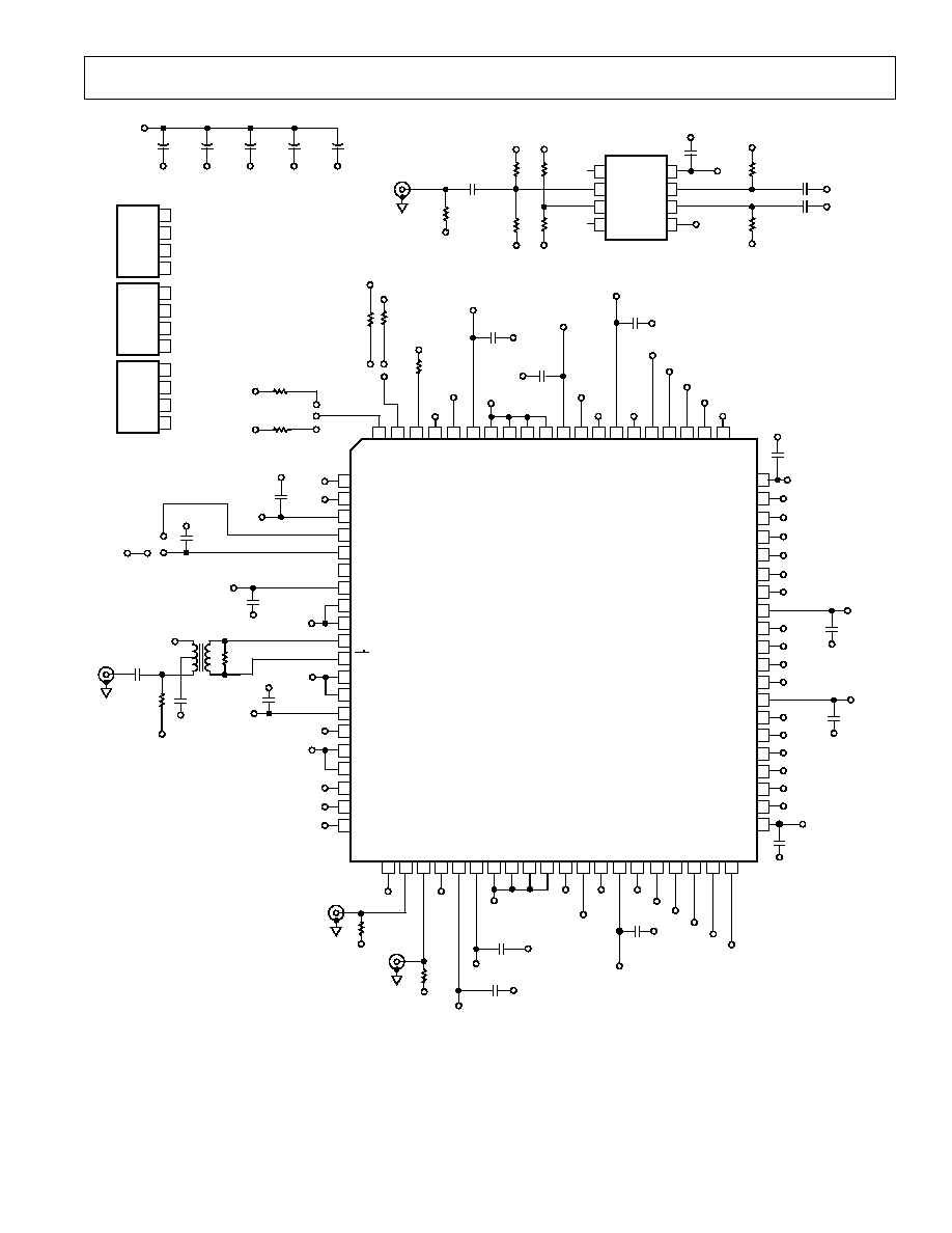
ENCODE
AGND
NOTE:
R3, R6, R7, R24 OPTIONAL
(CAN BE ZERO )
DB3
Figure 13a. PCB Schematic
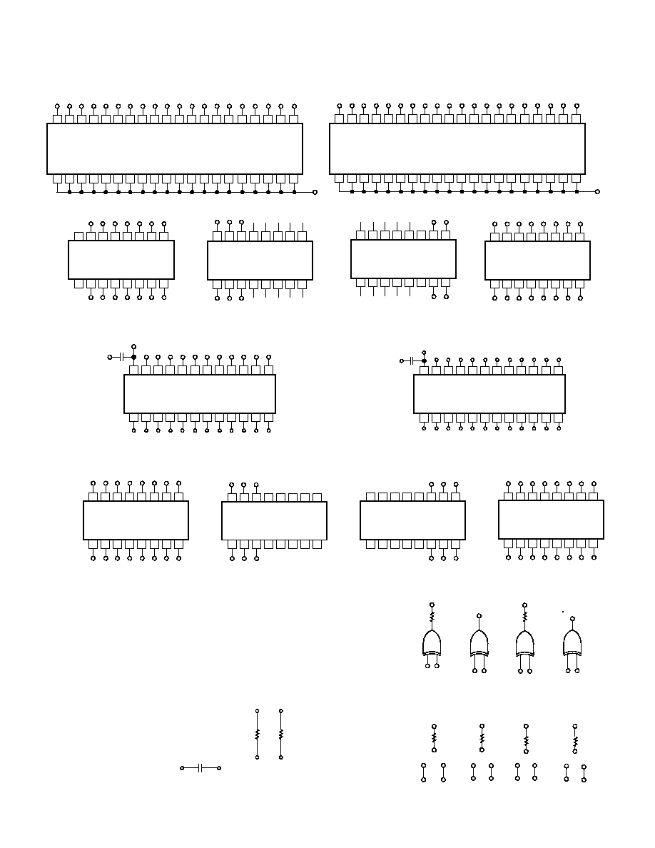
REV. 0
AD9410
16
2
4
6
8
10
12
14
16
18
20
22
24
26
28
30
32
34
36
38
40
P3
1
3
5
7
9
11
13
15
17
19
21
23
25
27
29
31
33
35
37
39
GND
DRB
GND
DN9
DN8
DN7
DN6
DN5
DN4
DN3
DN1
DN2
DN0
GND
GND
GND
GND
GND
GND
GND
GND
HEADER 40
2
4
6
8
10
12
14
16
18
20
22
24
26
28
30
32
34
36
38
40
GND
P2
1
3
5
7
9
11
13
15
17
19
21
23
25
27
29
31
33
35
37
39
GND
DRA
GND
DM9
DM8
DM7
DM6
DM5
DM4
DM3
DM1
DM2
DM0
GND
GND
GND
GND
GND
GND
GND
HEADER 40
8
7
6
5
4
3
2
1
R38
9
10
11
12
13
14
15
16
DN7
DN6
DN5
DN4
DN3
DN2
DN1
DN0
D7B
D6B
D5B
D4B
D3B
D2B
D1B
D0B
1A
2A
3A
4A
5A
6A
7A
8A
1B
2B
3B
4B
5B
6B
7B
8B
RPACK
8
7
6
5
4
3
2
1
R28
9
10
11
12
13
14
15
16
NC
NC
NC
NC
NC
DN9
DN8
1A
2A
3A
4A
5A
6A
7A
8A
1B
2B
3B
4B
5B
6B
7B
8B
RPACK
NC
NC
NC
NC
NC
D9B
D8B
8
7
6
5
4
3
2
1
R36
9
10
11
12
13
14
15
16
DM2
DM1
DM0
NC
NC
NC
NC
1A
2A
3A
4A
5A
6A
7A
8A
1B
2B
3B
4B
5B
6B
7B
8B
RPACK
D2A
D1A
D0A
NC
NC
NC
NC
NC
NC
8
7
6
5
4
3
2
1
R34
9
10
11
12
13
14
15
16
DM9
DM8
DM7
DM6
DM5
DM4
DM3
D9A
D8A
D7A
D6A
D5A
D4A
D3A
1A
2A
3A
4A
5A
6A
7A
8A
1B
2B
3B
4B
5B
6B
7B
8B
RPACK
12
11
10
9
8
7
6
5
4
3
2
1
U5
13
14
15
16
17
18
19
20
21
22
23
24
D9B
D8B
D7B
D6B
D5B
D4B
D3B
D2B
D1B
CLKB
D0B
GND
DY9
DY8
DY7
DY6
DY5
DY4
DY3
DY2
DY1
GND
DY0
VCC
Y0
Y1
Y2
Y3
Y4
Y5
Y6
Y7
Y8
CLK
Y9
DE
X0
X1
X2
X3
X4
X5
X6
X7
X8
GND
X9
C39
0.1
F
74LCXB21
GND
VDD
12
11
10
9
8
7
6
5
4
3
2
1
U4
13
14
15
16
17
18
19
20
21
22
23
24
VDD
D9A
D8A
D7A
D6A
D5A
D4A
D3A
D2A
D1A
CLKA
D0A
VCC
Y0
Y1
Y2
Y3
Y4
Y5
Y6
Y7
Y8
CLK
Y9
DE
X0
X1
X2
X3
X4
X5
X6
X7
X8
GND
X9
C37
0.1
F
74LCXB21
GND
GND
DX9
DX8
DX7
DX6
DX5
DX4
DX3
DX2
DX1
GND
DX0
8
7
6
5
4
3
2
1
R39
9
10
11
12
13
14
15
16
DY7
DY6
DY5
DY4
DY3
DY2
DY1
DY0
DB7
DB6
DB5
DB4
DB3
DB2
DB1
DB0
1A
2A
3A
4A
5A
6A
7A
8A
1B
2B
3B
4B
5B
6B
7B
8B
RPACK
8
7
6
5
4
3
2
1
R29
9
10
11
12
13
14
15
16
DYOR
DY9
DY8
DBOR
DB9
DB8
1A
2A
3A
4A
5A
6A
7A
8A
1B
2B
3B
4B
5B
6B
7B
8B
RPACK
8
7
6
5
4
3
2
1
R40
9
10
11
12
13
14
15
16
DX2
DX1
DX0
DA2
DA1
DA0
1A
2A
3A
4A
5A
6A
7A
8A
1B
2B
3B
4B
5B
6B
7B
8B
RPACK
8
7
6
5
4
3
2
1
R32
9
10
11
12
13
14
15
16
DXOR
DX9
DX8
DX7
DX6
DX4
DX3
1A
2A
3A
4A
5A
6A
7A
8A
1B
2B
3B
4B
5B
6B
7B
8B
RPACK
DAOR
DA9
DA8
DA7
DA6
DA4
DA3
DA5
DX5
DRA
R44
00
3
U9
74AC86
1
2
DCOTA
XORA
VDD
E24
GND
E18
E17
R2
100
XORA
VDD
E26
GND
E28
E27
R37
100
XORB
CLKA
6
U9
74AC86
4
5
DCOTA
XORB
VDD
E23
GND
E22
E25
R43
100
XORD
CLKB
8
U9
9
10
DCOTA
XORD
74AC86
VDD
E20
GND
E21
E19
R42
100
XORC
DRB
R45
00
11
U9
74AC86
12
13
DCOCA
XORC
VDD
GND
C32
0.1
F
DCOT
DCOTA
R16
00
DCOC
DCOCA
R17
00
Figure 13b. PCB Schematic (Continued)
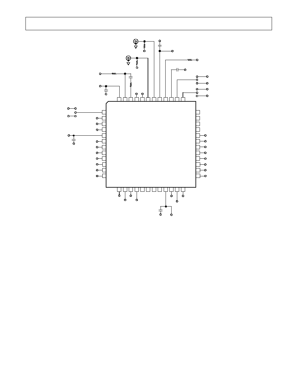
REV. 0
AD9410
17
TROUBLESHOOTING
If the board does not seem to be working correctly, try the
following:
·
Verify power at IC pins.
·
Check that all jumpers are in the correct position for the
desired mode of operation.
·
Verify VREF is at 2.5 V.
· Try running encode clock and analog input at low speeds
(10 MSPS/1 MHz) and monitor latch outputs, DAC outputs,
and ADC outputs for toggling.
The AD9410 Evaluation Board is provided as a design example
for customers of Analog Devices, Inc. ADI makes no warranties,
express, statutory, or implied, regarding merchantability or
fitness for a particular purpose.
AD9751
U2
E34
GND
E33
DCOCA
DCOTA
GND
C13
0.1 F
GND
DM9
DM8
DM7
DM6
DM5
DM4
E35
DN0
DN1
DN2
DN3
DN4
DN5
DN6
DN7
DN8
DN9
GND
C17
0.1 F
GND
VDAC
DM0
DM1
DM2
DM3
E29
E31
VDAC
E30
GND
E2
VDAC
E5
GND
E4
C23
0.1 F
GND
R10
2k
GND
C3
0.1 F
VDAC
GND
C20
0.1 F
R13
392
GND GND
R12
50
GND
R1
50
GND
J4
1
2
3
4
5
6
7
8
9
11
12
10
13
14
15
16
17
18
19
20
21
23
24
22
36
35
34
33
32
31
30
29
28
26
25
27
48
47
46
45
44
43
42
41
40
38
37
39
VDAC
R5
392
GND
GND
VDAC
VDAC
C33
1 F
VDAC
E32
J3
GND
Figure 13c. PCB Schematic (Continued)
REV. 0
AD9410
18
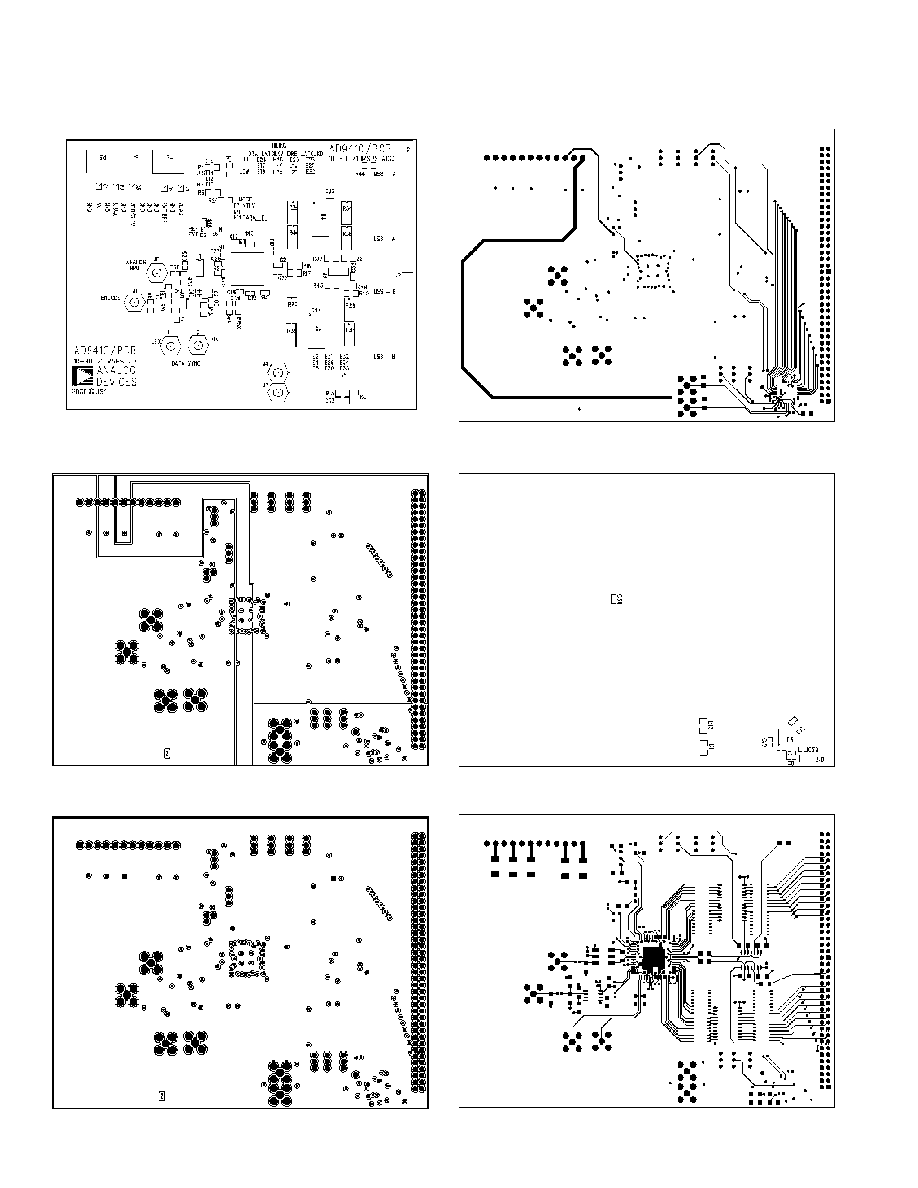
Figure 14. Top Silkscreen
Figure 15. Split Power Plane
Figure 16. Ground Plane
EVALUATION BOARD LAYOUT
Figure 17. Bottom Components and Routing
Figure 18. Bottom Silkscreen
Figure 19. Top Components and Routing

REV. 0
AD9410
19
AD9410 Evaluation Board Bill of Material
Quantity
Reference Description
Device
Package
Value
5
C1C5
Capacitor
TAJD
10
µF
29
C6C30, C32, C37, C39, C40
Capacitor
603
0.1
µF
1
C33
Capacitor
1206
1
µF
31
E1E7, E10E12, E14, E16E35
Ehole
6
J1, J3, J4, J8, J9X, J10X
SMB
3
P1, P4, P5
4-Pin Power
25.531.3425.0
Wieland
Connector
25.602.5453.0
2
P2, P3
40-Pin Header
7
R1, R8, R12, R23
*, R25X, R26, R27
Resistor
1206
50
8
R2, R3, R4, R6, R24, R37, R42, R43
Resistor
1206
100
1
R13
Resistor
1206
392
1
R7
Resistor
1206
100
2
R9, R18
Resistor
1206
24 k
1
R10
Resistor
1206
2 k
2
R11, R15
Resistor
1206
330
2
R14, R19
Resistor
1206
8.2 k
5
R5, R16, R17, R44, R45
Resistor
1206
0
8
R28, R29, R32, R34, R36, R38R40
RPACK
766163220G
CTS
22
1
T1
Transformer (1:1)
ADT1-1WT
Minicircuits
1
U1
MC10EL16
SOIC8
1
U2
AD9751
LQFP48
1
U3
AD9410
LQFP80
2
U4, U5
74LCX821
SOIC24
1
U9
74AC86
SOIC14
*Optional R23 not placed on board (50
termination resistor).
REV. 0
20
C016794.510/00 (rev. 0)
PRINTED IN U.S.A.
AD9410
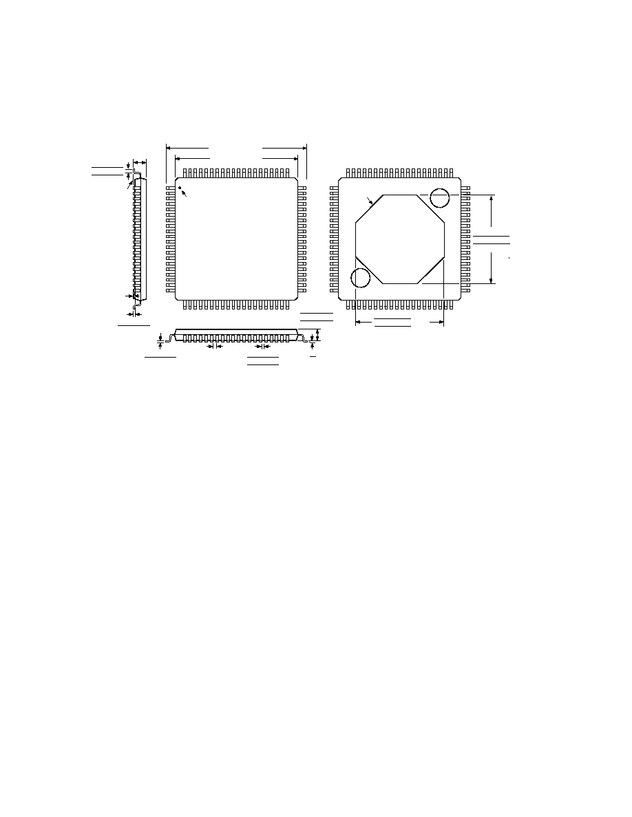
OUTLINE DIMENSIONS
Dimensions shown in inches and (mm).
80-Lead PowerQuad 2 (LQFP_ED)
(SQ-80)
1
20
21
41
40
60
80
61
PIN 1
TOP VIEW
(PINS
DOWN)
0.630 (16.00) SQ
0.551 (14.00) SQ
SEATING
PLANE
0.063 (1.60)
MAX
0.004 (0.10)
MAX
COPLANARITY
0.006 (0.15)
0.002 (0.05)
0.030 (0.75)
0.024 (0.60)
0.018 (0.45)
0.0256 (0.65)
BSC
7
0
0.008 (0.20)
0.004 (0.09)
0.015 (0.38)
0.013 (0.32)
0.009 (0.22)
0.057 (1.45)
0.055 (1.40)
0.053 (1.35)
CONTROLLING DIMENSION IN MILLIMETERS.
CENTER FIGURES ARE TYPICAL UNLESS
OTHERWISE NOTED.
1
20
21
41
40
60
80
61
XX
BOTTOM
VIEW
NICKEL PLATED
0.120 (3.04) 45 C CHAMFER
4 PLACES
0.413 (10.50)
0.394 (10.00) REF
0.374 (9.50)
0.413 (10.50)
0.394 (10.00) REF
0.374 (9.50)
NOTE
The AD9410 has a conductive heat slug to help dissipate heat
and ensure reliable operation of the device over the full indus-
trial temperature range. The slug is exposed on the bottom of
the package. It is recommended that no PCB traces or vias be
located under the package that could come in contact with the
conductive slug. Attaching the slug to a ground plane while not
required in most applications will reduce the junction tempera-
ture of the device which may be beneficial in high temperature
environments.