AD9396 Analog/DVI Dual-Display Interface Data Sheet (Rev. 0)
Analog/DVI
Dual-Display Interface
AD9396
Rev. 0
Information furnished by Analog Devices is believed to be accurate and reliable.
However, no responsibility is assumed by Analog Devices for its use, nor for any
infringements of patents or other rights of third parties that may result from its use.
Specifications subject to change without notice. No license is granted by implication
or otherwise under any patent or patent rights of Analog Devices. Trademarks and
registered trademarks are the property of their respective owners.
One Technology Way, P.O. Box 9106, Norwood, MA 02062-9106, U.S.A.
Tel: 781.329.4700
www.analog.com
Fax: 781.461.3113
© 2005 Analog Devices, Inc. All rights reserved.
FEATURES
Analog/DVI dual interface
Supports high bandwidth digital content protection
RGB-to-YCbCr 2-way color conversion
Automated clamping level adjustment
1.8 V/3.3 V power supply
100-lead, Pb-free LQFP
RGB and YCbCr output formats
Analog interface
8-bit triple ADC
150 MSPS maximum conversion rate
Macrovision® detection
2:1 input mux
Full sync processing
Sync detect for hot plugging
Midscale clamping
Digital video interface
DVI 1.0
150 MHz DVI receiver
Supports HDCP 1.1
APPLICATIONS
Advanced TVs
HDTVs
Projectors
LCD monitors
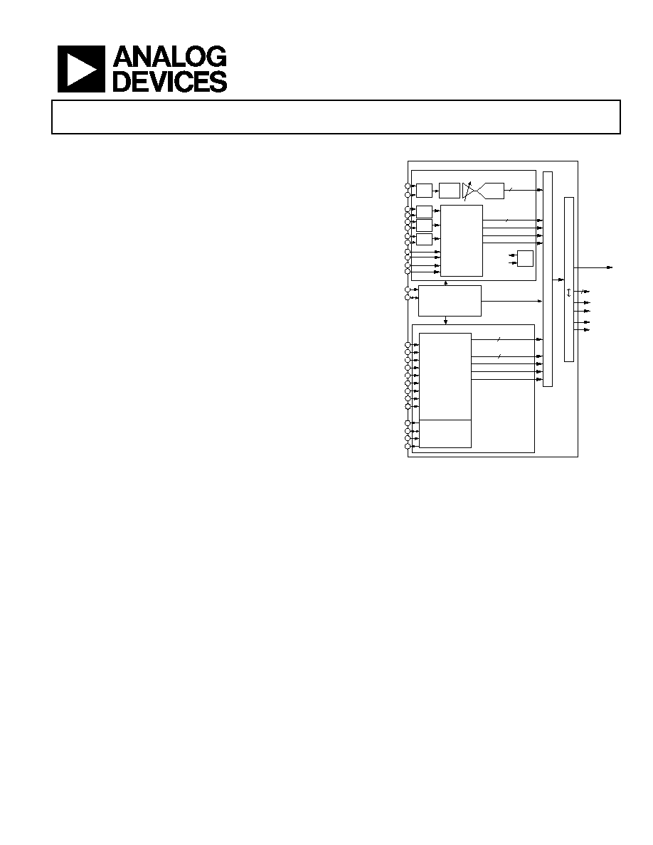
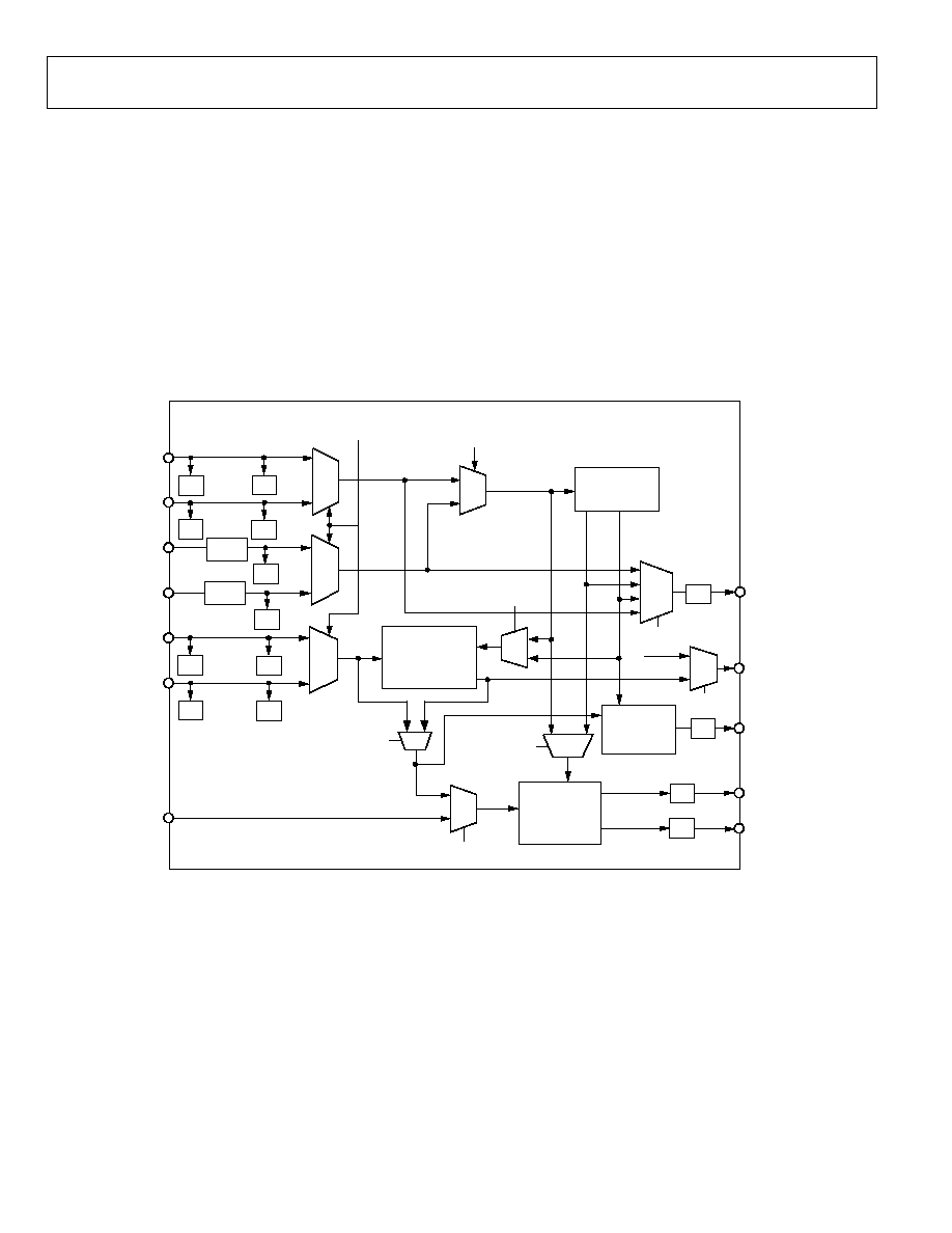
FUNCTIONAL BLOCK DIAGRAM
05690-001
DATACK
DE
VSYNC
SYNC
PROCESSING
AND
CLOCK
GENERATION
DATACK
2
REF
HSOUT
VSOUT
SOGOUT
DVI RECEIVER
DIGITAL INTERFACE
REFOUT
REFIN
CLAMP
A/D
2:1
MUX
2:1
MUX
2:1
MUX
2:1
MUX
2
HDCP
2
DATACK
HSOUT
VSOUT
SOGOUT
DE
MUXES
R/G/B 8 × 3
OR YCbCr
R/G/B 8 × 3
OR YCbCr
YCbCr (4:2:2
OR 4:4:4)
AD9396
R/G/B OR YPbPr
IN0
R/G/B OR YPbPr
IN1
HSYNC 0
HSYNC 1
HSYNC 0
HSYNC 1
SOGIN 0
SOGIN 1
COAST
CKINV
CKEXT
FILT
SCL
SDA
Rx1+
Rx1
Rx2+
Rx2
RxC+
RxC
RTERM
MCL
MDA
DDCSCL
DDCSDA
Rx0+
Rx0
HSYNC
R/G/B 8 × 3
RG
B
Y
CbCr MATRIX
SERIAL REGISTER
AND
POWER MANAGEMENT
ANALOG INTERFACE
Figure 1.
GENERAL DESCRIPTION
The AD9396 offers designers the flexibility of an analog
interface and digital visual interface (DVI) receiver integrated
on a single chip. Also included is support for high bandwidth
digital content protection (HDCP).
The AD9396 is a complete 8-bit, 150 MSPS monolithic analog
interface optimized for capturing component video (YPbPr)
and RGB graphics signals. Its 150 MSPS encode rate capability
and full power analog bandwidth of 330 MHz supports all
HDTV formats (up to 1080p and 720p) and FPD resolutions up
to SXGA (1280 × 1024 @ 80 Hz).
The analog interface includes a 150 MHz triple ADC with
internal 1.25 V reference, a phase-locked loop (PLL), program-
mable gain, offset, and clamp control. The user provides only
1.8 V and 3.3 V power supply, analog input, and HSYNC.
Three-state CMOS outputs may be powered from 1.8 V to 3.3V.
The on-chip PLL generates a pixel clock from HSYNC. Pixel
clock output frequencies range from 12 MHz to 150 MHz. PLL
clock jitter is typically less than 700 ps p-p at 150 MHz. The
AD9396 also offers full sync processing for composite sync and
sync-on-green (SOG) applications.
The AD9396 contains a DVI-compatible receiver and supports
all HDTV formats (up to 1080p and 720p) and display
resolutions up to SXGA (1280 × 1024 @ 80 Hz). The receiver
features an intrapair skew tolerance of up to one full clock cycle.
With the inclusion of HDCP, displays may now receive
encrypted video content. The AD9396 allows for authentication
of a video receiver, decryption of encoded data at the receiver,
and renewability of that authentication during transmission as
specified by the HDCP 1.1 protocol.
Fabricated in an advanced CMOS process, the AD9396 is pro-
vided in a space-saving, 100-lead, surface-mount, Pb-free plastic
LQFP and is specified over the 0ºC to 70ºC temperature range.

AD9396
Rev. 0 | Page 2 of 48
TABLE OF CONTENTS
Features .............................................................................................. 1
Applications....................................................................................... 1
Functional Block Diagram .............................................................. 1
General Description ......................................................................... 1
Specifications..................................................................................... 3
Analog Interface Electrical Characteristics............................... 3
Digital Interface Electrical Characteristics ............................... 4
Absolute Maximum Ratings............................................................ 6
Explanation of Test Levels ........................................................... 6
ESD Caution.................................................................................. 6
Pin Configuration and Function Descriptions............................. 7
Design Guide................................................................................... 11
General Description................................................................... 11
Digital Inputs .............................................................................. 11
Analog Input Signal Handling.................................................. 11
HSYNC and VSYNC Inputs...................................................... 11
Serial Control Port ..................................................................... 11
Output Signal Handling............................................................. 11
Clamping ..................................................................................... 11
Timing.......................................................................................... 15
DVI Receiver............................................................................... 19
DE Generator .............................................................................. 19
4:4:4 to 4:2:2 Filter ...................................................................... 19
Timing Diagrams........................................................................ 20
2-Wire Serial Register Map ........................................................... 21
2-Wire Serial Control Register Details ........................................ 29
Chip Identification ..................................................................... 29
PLL Divider Control .................................................................. 29
Clock Generator Control .......................................................... 29
Input Gain ................................................................................... 30
Input Offset ................................................................................. 30
Sync .............................................................................................. 30
Coast and Clamp Controls........................................................ 31
Status of Detected Signals ......................................................... 31
Polarity Status ............................................................................. 32
BT656 Generation ...................................................................... 36
Macrovision................................................................................. 36
Color Space Conversion ............................................................ 37
2-Wire Serial Control Port ............................................................ 39
PCB Layout Recommendations.................................................... 41
Analog Interface Inputs ............................................................. 41
Power Supply Bypassing ............................................................ 41
PLL ............................................................................................... 41
Outputs (Both Data and Clocks).............................................. 42
Digital Inputs .............................................................................. 42
Color Space Converter (CSC) Common Settings...................... 43
Outline Dimensions ....................................................................... 45
Ordering Guide .......................................................................... 45
REVISION HISTORY
10/05--Revision 0: Initial Version

AD9396
Rev. 0 | Page 3 of 48
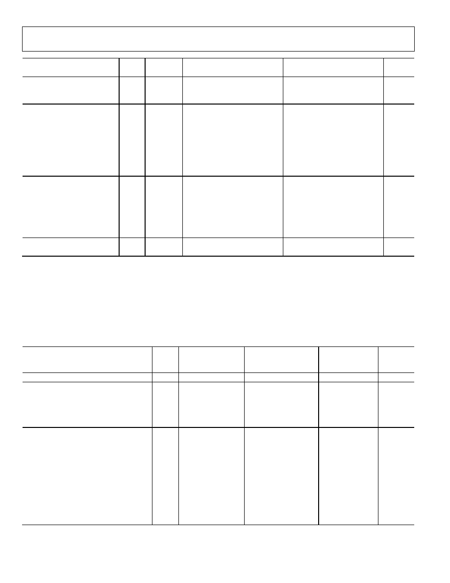
SPECIFICATIONS
ANALOG INTERFACE ELECTRICAL CHARACTERISTICS
V
DD,
V
D
= 3.3 V, DV
DD
= PV
DD
= 1.8 V, ADC clock = maximum.
Table 1.
AD9396KSTZ-100
AD9396KSTZ-150
Parameter
Temp
Test
Level
Min Typ
Max
Min Typ
Max
Unit
RESOLUTION
8
8
Bits
DC
ACCURACY
Differential
Nonlinearity
25°C
I 0.6
+1.6/1.0
±0.7
+1.8/1.0
LSB
Integral
Nonlinearity
25°C
I ±1.0
±2.1
±1.1
±2.25
LSB
No Missing Codes
Full
Guaranteed
Guaranteed
ANALOG
INPUT
Input
Voltage
Range
Minimum
Full
VI
0.5
0.5
V
pp
Maximum
Full
VI 1.0 1.0 V
pp
Gain
Tempco
25°C
V
100
220
ppm/°C
Input Bias Current
25°C
V
0.2
1
A
Input Full-Scale Matching
25C
Full
VI
VI
1.25
1.50
5
7
1.25
1.50
5
7
%FS
%FS
Offset Adjustment Range
Full
V
50
50
%FS
SWITCHING PERFORMANCE
1
Maximum Conversion Rate
Full
VI
100
150
MSPS
Minimum Conversion Rate
Full
VI
10
10
MSPS
Data to Clock Skew
Full
IV
-0.5
+2.0
-0.5
+2.0
ns
SERIAL
PORT
TIMING
t
BUFF
Full
VI 4.7 4.7 s
t
STAH
Full
VI 4.0 4.0 s
t
DHO
Full
VI 0
0
s
t
DAL
Full
VI 4.7 4.7 s
t
DAH
Full
VI 4.0 4.0 s
t
DSU
Full
VI 250 250 ns
t
STASU
Full
VI 4.7 4.7 s
t
STOSU
Full
VI 4.0 4.0 s
HSYNC Input Frequency
Full
VI
15
110
15
110
KHz
Maximum PLL Clock Rate
Full
VI
100
150
MHz
Minimum PLL Clock Rate
Full
IV
12
12
MHz
PLL Jitter
25°C
IV
700
700
ps p-p
Sampling Phase Tempco
Full
IV
15
15
ps/°C
DIGITAL
INPUTS
(5
V
Tolerant)
Input Voltage, High (V
IH
)
Full
VI 2.6 2.6 V
Input Voltage, Low (V
IL
)
Full
VI
0.8
0.8
V
Input Current, High (I
IH
)
Full
V
-82
-82
A
Input Current, Low (I
IL
)
Full
V
82
82
A
Input
Capacitance 25°C
V
3
3
pF
DIGITAL
OUTPUTS
Output Voltage, High (V
OH
) Full VI
V
DD
- 0.1
V
DD
- 0.1
V
Output Voltage, Low (V
OL
)
Full
VI
0.4
0.4
V
Duty Cycle, DATACK
Full
V
45
50
55
45
50
55
%
Output Coding
Binary
Binary
AD9396
Rev. 0 | Page 4 of 48
AD9396KSTZ-100
AD9396KSTZ-150
Parameter
Temp
Test
Level
Min Typ
Max
Min Typ
Max
Unit
POWER
SUPPLY
V
D
Supply
Voltage
Full
IV 3.15 3.3
3.47
3.15 3.3
3.47
V
DV
DD
Supply
Voltage Full
IV 1.7 1.8
1.9
1.7 1.8
1.9
V
V
DD
Supply
Voltage
Full
IV 1.7 3.3
3.47
1.7 3.3
3.47
V
PV
DD
Supply
Voltage Full
IV 1.7 1.8
1.9
1.7 1.8
1.9
V
I
D
Supply Current (V
D
)
25°C
VI
260
300
330
mA
I
DVDD
Supply Current (DV
DD
)
25°C
VI
45
60
85
mA
I
DD
Supply Current (V
DD
)
2
25°C VI
37
100
3
130
3
mA
IP
VDD
Supply Current (P
VDD
)
25°C
VI
10
15
20
mA
Total
Power
Full
VI
1.1
1.4
1.15
1.4
W
Power-Down
Dissipation
Full
VI
130
130
mW
DYNAMIC
PERFORMANCE
Analog Bandwidth, Full
Power
25°C
V
330
330
MHz
Signal-to-Noise
Ratio
(SNR)
25°C
I 46
46
dB
Without
Harmonics
f
IN
= 40.7 MHz
Full
V
45
45
dB
Crosstalk
Full
V
60
60
dBc
THERMAL
CHARACTERISTICS
JA
Junction-to-Ambient
V
35
35
°C/W
1
Drive strength = high.
2
DATACK load = 15 pF, data load = 5 pF.
3
Specified current and power values with a worst-case pattern (on/off).
DIGITAL INTERFACE ELECTRICAL CHARACTERISTICS
V
DD
= V
D
= 3.3 V, DV
DD
= PV
DD
= 1.8 V, ADC clock = maximum.
Table 2.
AD9396KSTZ-100
AD9396KSTZ-150
Parameter
Test
Level
Conditions Min
Typ
Max
Min
Typ
Max
Unit
RESOLUTION
8
8
Bit
DC DIGITAL I/O Specifications
High Level Input Voltage, (V
IH
) VI
2.5
2.5
V
Low Level Input Voltage, (V
IL
) VI
0.8
0.8
V
High Level Output Voltage, (V
OH
) VI
V
DD
- 0.1
V
Low Level Output Voltage, (V
OL
) VI
V
DD
- 0.1
0.1
0.1
V
DC SPECIFICATIONS
Output High Level
IV
Output drive = high
36
36
mA
(I
OHD
) (V
OUT
= V
OH
)
IV
Output drive = low
24
24
mA
Output Low Level
IV
Output drive = high
12
12
mA
I
OLD
, (V
OUT
= V
OL
)
IV
Output drive = low
8
8
mA
DATACK High Level
IV
Output drive = high
40
40
mA
V
OHC
, (V
OUT
= V
OH
)
IV
Output drive = low
20
20
mA
DATACK Low Level
IV
Output drive = high
30
30
mA
V
OLC
, (V
OUT
= V
OL
)
IV
Output drive = low
15
15
mA
Differential Input Voltage, Single-
Ended Amplitude
IV
75
700
75
700
mV
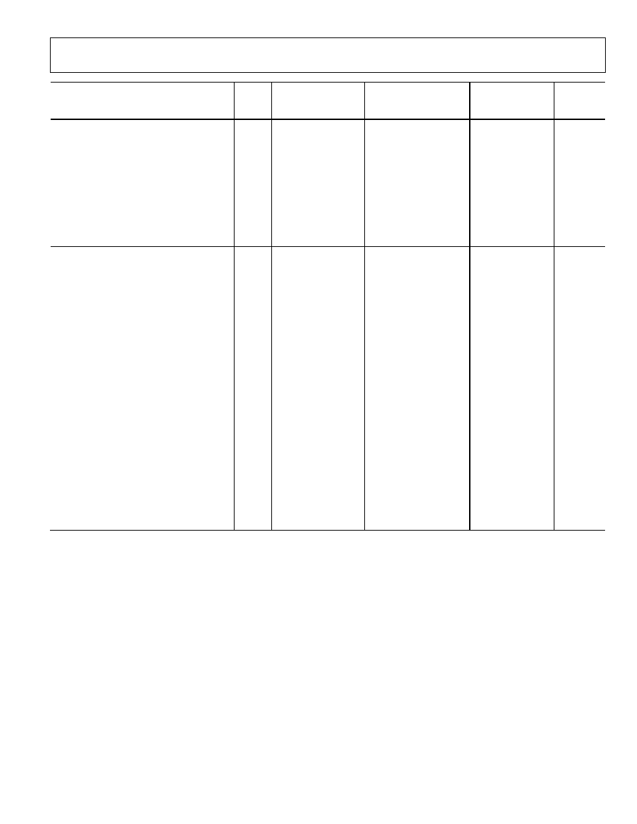
AD9396
Rev. 0 | Page 5 of 48
AD9396KSTZ-100
AD9396KSTZ-150
Parameter
Test
Level
Conditions Min
Typ
Max
Min
Typ
Max
Unit
POWER SUPPLY
V
D
Supply Voltage
IV
3.15
3.3
3.47
3.15
3.3
3.47
V
V
DD
Supply
Voltage
IV
1.7
3.3 347 1.7 3.3 347 V
DV
DD
Supply Voltage
IV
1.7
1.8
1.9
1.7
1.8
1.9
V
PV
DD
Supply Voltage
IV
1.7
1.8
1.9
1.7
1.8
1.9
V
I
VD
Supply Current (Typical Pattern)
1
V
80
100
80
110
mA
I
VDD
Supply Current (Typical Pattern)
2
V
40
100
3
55
175
3
mA
I
DVDD
Supply Current (Typical Pattern)
1, 4
V
88
110
110
145
mA
I
PVDD
Supply Current (Typical Pattern)
1
V
26
35
30
40
mA
Power-Down Supply Current (I
PD
) VI
130
130
mA
AC SPECIFICATIONS
Intrapair (+ to -) Differential Input Skew
(T
DPS
)
IV
360
ps
Channel-to-Channel Differential Input
Skew (T
CCS
)
IV
6
Clock
Period
Low-to-High Transition Time for Data and
Controls (D
LHT
)
IV
Output drive = high;
C
L
= 10 pF
900
ps
IV
Output drive = low;
C
L
= 5 pF
1300
ps
Low-to-High Transition Time for
DATACK (D
LHT
)
IV
Output drive = high;
C
L
= 10 pF
650
ps
IV
Output drive = low;
C
L
= 5 pF
1200
ps
High-to-Low Transition Time for Data and
Controls (D
HLT
)
IV
Output drive = high;
C
L
= 10 pF
850
ps
IV
Output drive = low;
C
L
= 5 pF
1250
ps
High-to-Low Transition Time for
DATACK (D
HLT
)
IV
Output drive = high;
C
L
= 10 pF
800
ps
IV
Output drive = low;
C
L
= 5 pF
1200
ps
Clock to Data Skew
5
(T
SKEW
) IV
0.5
+2.0
0.5
2.0
ns
Duty Cycle, DATACK
5
IV
45
50
55
%
DATACK Frequency (F
CIP
) VI
20
150
MHz
1
The typical pattern contains a gray scale area, output drive = high. Worst-case pattern is alternating black and white pixels.
2
The typical pattern contains a gray scale area, output drive = high.
3
Specified current and power values with a worst-case pattern (on/off).
4
DATACK load = 10 pF, data load = 5 pF.
5
Drive strength = high.
AD9396
Rev. 0 | Page 6 of 48
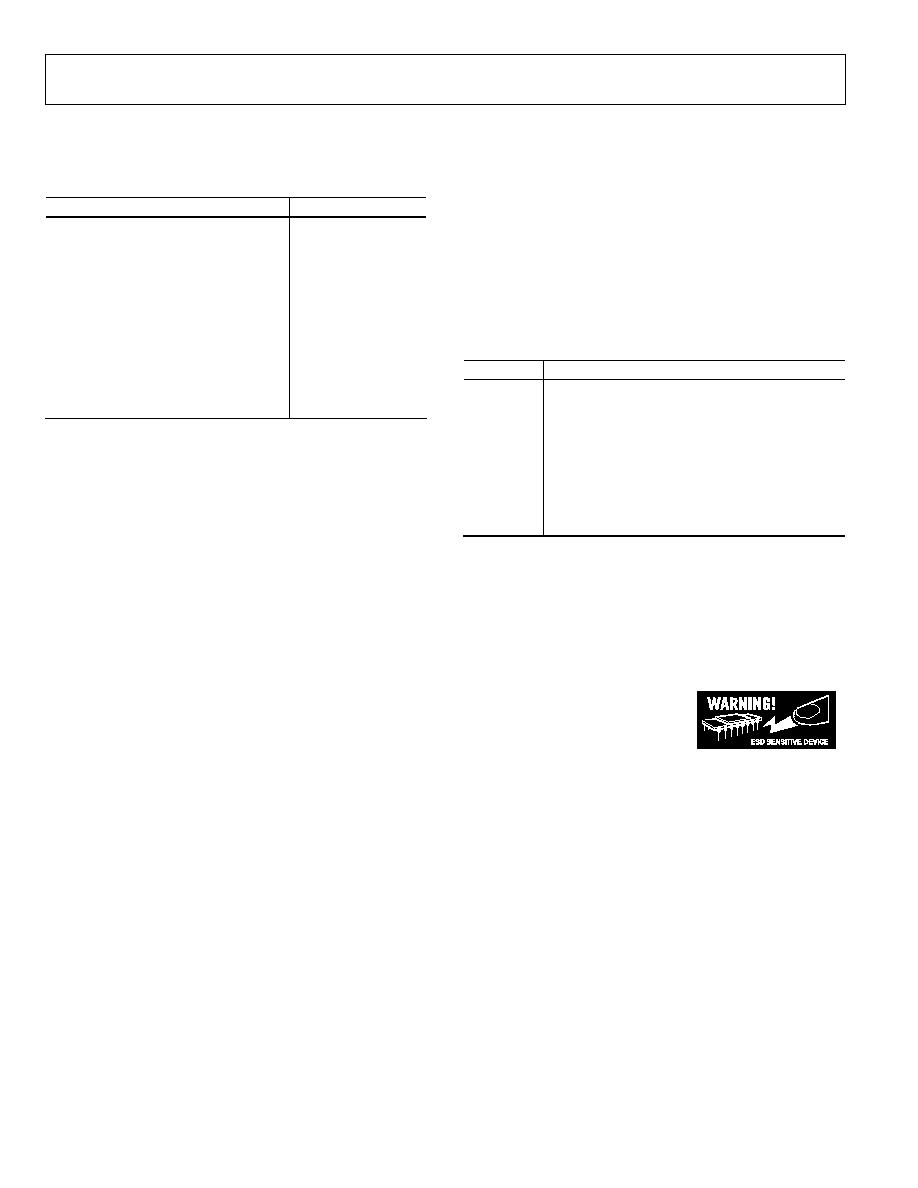
ABSOLUTE MAXIMUM RATINGS
Table 3.
Stresses above those listed under Absolute Maximum Ratings
may cause permanent damage to the device. This is a stress
rating only; functional operation of the device at these or any
other conditions above those indicated in the operational
section of this specification is not implied. Exposure to absolute
maximum rating conditions for extended periods may affect
device reliability.
EXPLANATION OF TEST LEVELS
Table 4.
Level Test
I
100% production tested.
II
100% production tested at 25°C and sample
tested at specified temperatures.
III
Sample tested only.
IV
Parameter is guaranteed by design and
characterization testing.
V
Parameter is a typical value only.
VI
100% production tested at 25°C; guaranteed by
design and characterization testing.
ESD CAUTION
ESD (electrostatic discharge) sensitive device. Electrostatic charges as high as 4000 V readily accumulate on
the human body and test equipment and can discharge without detection. Although this product features
proprietary ESD protection circuitry, permanent damage may occur on devices subjected to high energy
electrostatic discharges. Therefore, proper ESD precautions are recommended to avoid performance
degradation or loss of functionality.
Parameter Rating
V
D
3.6 V
V
DD
3.6 V
DV
DD
1.98 V
PV
DD
1.98 V
Analog Inputs
V
D
to 0.0 V
Digital Inputs
5 V to 0.0 V
Digital Output Current
20 mA
Operating Temperature Range
-25°C to +85°C
Storage Temperature Range
-65°C to +150°C
Maximum Junction Temperature
150°C
Maximum Case Temperature
150°C
AD9396
Rev. 0 | Page 7 of 48
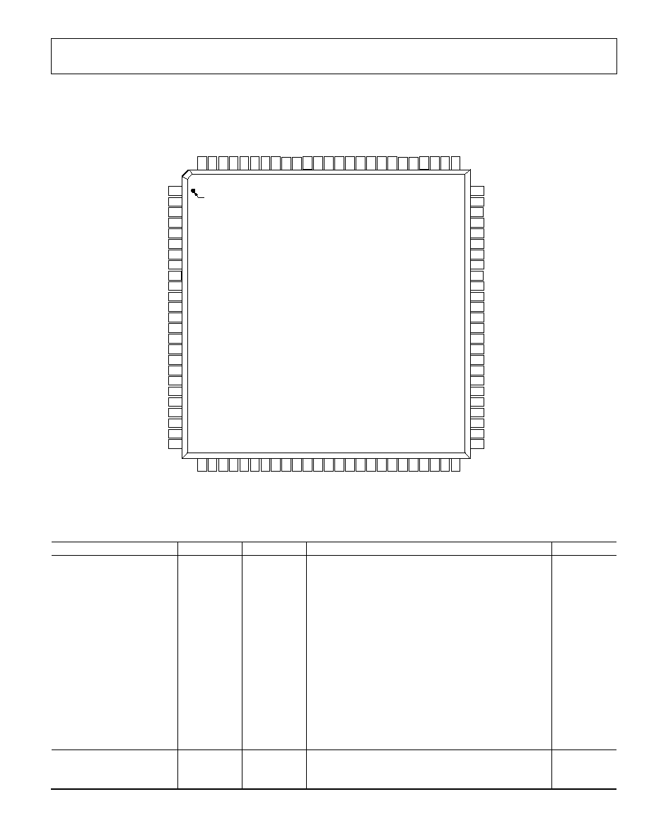
PIN CONFIGURATION AND FUNCTION DESCRIPTIONS
05690-002
V
DD
RE
D 0
RE
D 1
RE
D 2
RE
D 3
RE
D 4
RE
D 5
RE
D 6
RE
D 7
GND
V
DD
DATACK
DE
HS
OUT
SOGOUT
VSOU
T
O/E FIELD
SD
A
SC
L
P
W
RDN
V
D
R
AIN0
GND
R
AIN1
V
D
26
CTL1
27
CTL0
28
NC
29
GND
30
DV
DD
31
GND
32
DV
DD
33
V
D
34
R
x0
35
R
x0+
36
GND
37
R
x1
38
R
x1+
39
GND
2
GREEN 7
3
GREEN 6
4
GREEN 5
7
GREEN 2
6
GREEN 3
5
GREEN 4
1
GND
8
GREEN 1
9
GREEN 0
10
V
DD
12
BLUE 7
13
BLUE 6
14
BLUE 5
15
BLUE 4
16
BLUE 3
17
BLUE 2
18
BLUE 1
19
BLUE 0
20
NC
NC = NO CONNECT
21
NC
22
NC
23
NC
24
CTL3
25
CTL2
11
GND
74
G
AIN0
GND
73
SOGIN 0
72
V
D
69
GND
70
SOGIN 1
71
G
AIN1
75
68
B
AIN0
67
V
D
66
B
AIN1
64
HSYNC 0
63
HSYNC 1
62
EXTCLK/COAST
61
VSYNC 0
60
VSYNC 1
59
PV
DD
58
PGND
57
FILT
56
PV
DD
55
PGND
54
PV
DD
53
GND
52
MDA
51
MCL
65
GND
40
R
x2
41
R
x2+
42
GND
43
Rx
C+
44
Rx
C
45
V
D
46
RTE
R
M
47
GND
48
DV
DD
49
DDCS
CL
50
DDCS
DA
100
99
98
97
96
95
94
93
92
91
90
89
88
87
86
85
84
83
82
81
80
79
78
77
76
PIN 1
AD9396
TOP VIEW
(Not to Scale)
Figure 2. Pin Configuration
Table 5. Complete Pinout List
Pin Type
Pin No.
Mnemonic
Function
Value
INPUTS 79
R
AIN0
Analog Input for Converter R Channel 0
0.0 V to 1.0 V
77
R
AIN1
Analog Input for Converter R Channel 1
0.0 V to 1.0 V
74
G
AIN0
Analog Input for Converter G Channel 0
0.0 V to 1.0 V
71
G
AIN1
Analog Input for Converter G Channel 1
0.0 V to 1.0 V
68
B
B
AIN0
Analog Input for Converter B Channel 0
0.0 V to 1.0 V
66
B
B
AIN1
Analog Input for Converter B Channel 1
0.0 V to 1.0 V
64
HSYNC 0
Horizontal SYNC Input for Channel 0
3.3 V CMOS
63
HSYNC 1
Horizontal SYNC Input for Channel 1
3.3 V CMOS
61
VSYNC 0
Vertical SYNC Input for Channel 0
3.3 V CMOS
60
VSYNC 1
Vertical SYNC Input for Channel 1
3.3 V CMOS
73
SOGIN 0
Input for Sync-on-Green Channel 0
0.0 V to 1.0 V
70
SOGIN 1
Input for Sync-on-Green Channel 1
0.0 V to 1.0 V
62
EXTCLK
External Clock Input--Shares Pin with COAST
3.3 V CMOS
62
COAST
PLL COAST Signal Input--Shares Pin with EXTCLK
3.3 V CMOS
81
PWRDN
Power-Down Control
3.3 V CMOS
OUTPUTS
92 to 99
RED [7:0]
Outputs of Red Converter, Bit 7 is MSB
V
DD
2 to 9
GREEN [7:0]
Outputs of Green Converter, Bit 7 is MSB
V
DD
12 to 19
BLUE [7:0]
Outputs of Blue Converter, Bit 7 is MSB
V
DD
AD9396
Rev. 0 | Page 8 of 48
Pin Type
Pin No.
Mnemonic
Function
Value
OUTPUTS
89
DATACK
Data Output Clock
V
DD
87
HSOUT
HSYNC Output Clock (Phase-Aligned with DATACK)
V
DD
85
VSOUT
VSYNC Output Clock (Phase-Aligned with DATACK)
V
DD
86
SOGOUT
SOG Slicer Output
V
DD
84
O/E FIELD
Odd/Even Field Output
V
DD
24, 25, 26, 27
CTL(3-0)
Control 3, 2, 1, and 0.
V
DD
REFERENCES
57
FILT
Connection for External Filter Components for PLL
POWER SUPPLY
80, 76, 72,
67, 45, 33
V
D
Analog Power Supply and DVI Terminators
3.3 V
100, 90, 10
V
DD
Output Power Supply
1.8 V to 3.3 V
59, 56, 54
PV
DD
PLL Power Supply
1.8 V
48, 32, 30
DV
DD
Digital Logic Power Supply
1.8 V
GND
Ground
0
V
CONTROL
83
SDA
Serial Port Data I/O
3.3 V CMOS
82
SCL
Serial Port Data Clock
3.3 V CMOS
HDCP
49
DDCSCL
HDCP Slave Serial Port Data Clock
3.3 V CMOS
50
DDCSDA
HDCP Slave Serial Port Data I/O
3.3 V CMOS
51
MCL
HDCP Master Serial Port Data Clock
3.3 V CMOS
52
MDA
HDCP Master Serial Port Data I/O
3.3 V CMOS
DIGITAL VIDEO DATA
35
Rx0+
Digital Input Channel 0 True
TMDS
34
Rx0-
Digital Input Channel 0 Complement
TMDS
38
Rx1+
Digital Input Channel 1 True
TMDS
37
Rx1-
Digital Input Channel 1 Complement
TMDS
41
Rx2+
Digital Input Channel 2 True
TMDS
40
Rx2-
Digital Input Channel 2 Complement
TMDS
DIGITAL VIDEO CLOCK
INPUTS
43
RxC+
Digital Data Clock True
TMDS
44
RxC-
Digital Data Clock Complement
TMDS
DATA ENABLE
88
DE
Data Enable
3.3 V CMOS
RTERM
46
RTERM
Sets Internal Termination Resistance
500
Table 6. Pin Function Descriptions
Mnemonic Description
INPUTS
R
AIN0
Analog Input for the Red Channel 0.
G
AIN0
Analog Input for the Green Channel 0.
B
B
AIN0
Analog Input for the Blue Channel 0.
R
AIN1
Analog Input for the Red Channel 1.
G
AIN1
Analog Input for the Green Channel 1.
B
B
AIN1
Analog Input for Blue Channel 1.
High impedance inputs that accept the red, green, and blue channel graphics signals, respectively. The three channels
are identical and can be used for any colors, but colors are assigned for convenient reference. They accommodate input
signals ranging from 0.5 V to 1.0 V full scale. Signals should be ac-coupled to these pins to support clamp operation
(see Figure 3 for an input reference circuit).
Rx0+
Digital Input Channel 0 True.
Rx0-
Digital Input Channel 0 Complement.
Rx1+
Digital Input Channel 1 True.
Rx1-
Digital Input Channel 1 Complement.
Rx2+
Digital Input Channel 2 True.
Rx2-
Digital input Channel 2 Complement.
These six pins receive three pairs of transition minimized differential signaling (TMDS) pixel data (at 10× the pixel rate)
from a digital graphics transmitter.
AD9396
Rev. 0 | Page 9 of 48
Mnemonic Description
RxC+
Digital Data Clock True.
RxC-
Digital Data Clock Complement.
This clock pair receives a TMDS clock at 1× pixel data rate.
HSYNC 0
Horizontal Sync Input Channel 0.
HSYNC 1
Horizontal Sync Input Channel 1.
These inputs receive a logic signal that establishes the horizontal timing reference and provides the frequency
reference for pixel clock generation. The logic sense of this pin is controlled by Serial Register 0x12, Bits 5:4 (HSYNC
polarity). Only the leading edge of HSYNC is active; the trailing edge is ignored. When HSYNC polarity = 0, the falling
edge of HSYNC is used. When HSYNC polarity = 1, the rising edge is active. The input includes a Schmitt trigger for
noise immunity.
VSYNC 0
Vertical Sync Input Channel 0.
VSYNC 1
Vertical Sync Input Channel 1.
These are the inputs for vertical sync.
SOGIN 0
Sync-on-Green Input Channel 0.
SOGIN 1
Sync-on-Green Input Channel 1.
These inputs are provided to assist with processing signals with embedded sync, typically on the green channel. The
pin is connected to a high speed comparator with an internally generated threshold. The threshold level can be
programmed in 10 mV steps to any voltage between 10 mV and 330 mV above the negative peak of the input signal.
The default voltage threshold is 150 mV. When connected to an ac-coupled graphics signal with embedded sync, it
produces a noninverting digital output on SOGOUT. (This is usually a composite sync signal, containing both vertical
and horizontal sync (HSYNC) information that must be separated before passing the horizontal sync signal to HSYNC.)
When not used, this input should be left unconnected. For more details on this function and how it should be
configured, refer to the HSYNC and VSYNC Inputs section.
EXTCLK/COAST
Coast Input to Clock Generator (Optional).
This input may be used to cause the pixel clock generator to stop synchronizing with HSYNC and continue producing a
clock at its current frequency and phase. This is useful when processing signals from sources that fail to produce
horizontal sync pulses during the vertical interval. The coast signal is generally not required for PC-generated signals.
The logic sense of this pin is controlled by coast polarity (Register 0x18, Bits 6:5). When not used, this pin may be
grounded and input coast polarity programmed to 1 (Register 0x18, Pin 5), or tied high (to V
D
through a 10 k resistor)
and input coast polarity programmed to 0. Input coast polarity defaults to 1 at power-up. This pin is shared with the
EXTCLK function, which does not affect coast functionality. For more details on coast, see the description in the Clock
Generation section.
EXTCLK/COAST External
Clock.
This allows the insertion of an external clock source rather than the internally generated PLL-locked clock. This pin is
shared with the coast function, does not affect EXTCLK functionality.
RTERM
RTERM is the termination resistor used to drive the AD9396 internally to a precise 50 termination for TMDS lines. This
should be a 500
1% tolerance resistor.
PWRDN
Power-Down Control/Three-State Control.
The function of this pin is programmable via Register 0x26 [2:1].
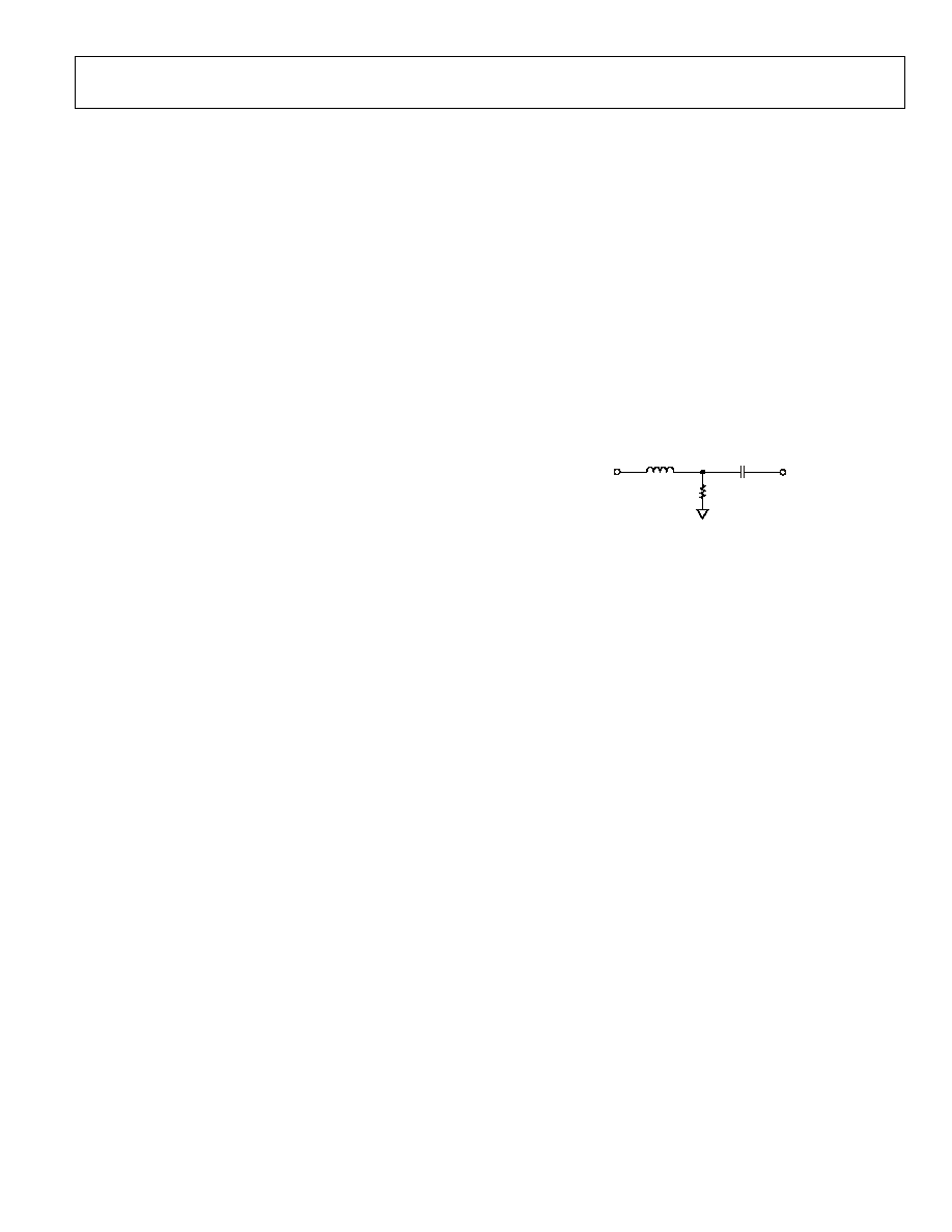
FILT
External Filter Connection.
For proper operation, the pixel clock generator PLL requires an external filter. Connect the filter shown in Figure 6 to
this pin. For optimal performance, minimize noise and parasitics on this node. For more information see the section on
PCB Layout Recommendations.
OUTPUTS
HSOUT
Horizontal Sync Output.
A reconstructed and phase-aligned version of the HSYNC input. Both the polarity and duration of this output can be
programmed via the serial bus registers. By maintaining alignment with DATACK and Data, data timing with respect to
horizontal sync can always be determined.
VSOUT
Vertical Sync Output.
The separated VSYNC from a composite signal or a direct passthrough of the VSYNC signal. The polarity of this output
can be controlled via serial bus bit (Register 0x24 [6]).
SOGOUT
Sync-on-Green Slicer Output.
This pin outputs one of four possible signals (controlled by Register 0x24 [2:1]): raw SOG, raw HSYNC, regenerated
HSYNC from the filter, or the filtered HSYNC. See Figure 8, the Sync Processing Block Diagram, to view how this pin is
connected. (Note: besides slicing off SOG, the output from this pin is not processed on the AD9396. VSYNC separation
is performed via the sync separator.
O/E FIELD
Odd/Even Field Bit for Interlaced Video. This output identifies whether the current field (in an interlaced signal) is odd
or even. The polarity of this signal is programmable via Register 0x24 [4].

AD9396
Rev. 0 | Page 10 of 48
Mnemonic Description
DATA ENABLE
Data Enable that defines valid video. Can be received in the signal or generated by the AD9396.
CTL(3 to 0)
Control 3, Control 2, Control 1, and Control 0 are output from the DVI stream. Refer to the DVI 1.0 specification for
explanation.
SERIAL PORT
SDA
Serial Port Data I/O for Programming AD9396 Registers--I
2
C® Address is 0x98.
SCL
Serial Port Data Clock for Programming AD9396 Registers.
DDCSDA
Serial Port Data I/O for HDCP Communications to Transmitter--I
2
C Address is 0x74 or 0x76.
DDCSCL
Serial Port Data Clock for HDCP Communications to Transmitter.
MDA
Serial Port Data I/O to EEPROM with HDCP Keys--I
2
C Address is 0xA0.
MCL
Serial Port Data Clock to EEPROM with HDCP Keys.
DATA OUTPUTS
Red [7:0]
Data Output, Red Channel.
Green [7:0]
Data Output, Green Channel.
Blue [7:0]
Data Output, Blue Channel.
The main data outputs. Bit 7 is the MSB. The delay from pixel sampling time to output is fixed, but is different if the
color space converter is used. When the sampling time is changed by adjusting the phase register, the output timing is
shifted as well. The DATACK and HSOUT outputs are also moved, so the timing relationship among the signals is
maintained.
DATA CLOCK
OUTPUT
DATACK
Data Clock Output.
This is the main clock output signal used to strobe the output data and HSOUT into external logic. Four possible output
clocks can be selected with Register 0x25 [7:6]. These are related to the pixel clock (1/2× pixel clock, 1× pixel clock, 2×
frequency pixel clock and a 90° phase shifted pixel clock) and they are produced either by the internal PLL clock
generator or EXTCLK and are synchronous with the pixel sampling clock. The polarity of DATACK can also be inverted
via Register 0x24 [0]. The sampling time of the internal pixel clock can be changed by adjusting the phase register.
When this is changed, the pixel-related DATACK timing is shifted as well. The DATA, DATACK, and HSOUT outputs are all
moved, so the timing relationship among the signals is maintained.
POWER SUPPLY
1
V
D
(3.3 V)
Analog Power Supply.
These pins supply power to the ADCs and terminators. They should be as quiet and filtered as possible.
V
DD
(1.8 V to 3.3 V)
Digital Output Power Supply.
A large number of output pins (up to 27) switching at high speed (up to 150 MHz) generates many power supply
transients (noise). These supply pins are identified separately from the V
D
pins, so take care to minimize output noise
transferred into the sensitive analog circuitry. If the AD9396 is interfacing with lower voltage logic, V
DD
may be
connected to a lower supply voltage (as low as 1.8 V) for compatibility.
PV
DD
(1.8 V)
Clock Generator Power Supply.
The most sensitive portion of the AD9396 is the clock generation circuitry. These pins provide power to the clock PLL
and help the user design for optimal performance. The designer should provide quiet, noise-free power to these pins.
DV
DD
(1.8 V)
Digital Input Power Supply.
This supplies power to the digital logic.
GND
Ground.
The ground return for all circuitry on-chip. It is recommended that the AD9396 be assembled on a single solid ground
plane, with careful attention to ground current paths.
1
The supplies should be sequenced such that V
D
and V
DD
are never less than 300 mV below DV
DD
. At no time should DV
DD
be more than 300 mV greater than V
D
or V
DD
.
AD9396
Rev. 0 | Page 11 of 48
DESIGN GUIDE
GENERAL DESCRIPTION
The AD9396 is a fully integrated solution for capturing analog
RGB or YUV signals and digitizing them for display on flat
panel monitors, projectors, or PDPs. In addition, the AD9396
has a digital interface for receiving DVI signals and is capable of
decoding HDCP-encrypted signals through connections to an
external EEPROM. The circuit is ideal for providing an
interface for HDTV monitors or as the front end to high
performance video scan converters.
Implemented in a high performance CMOS process, the
interface can capture signals with pixel rates of up to 150 MHz.
The AD9396 includes all necessary input buffering, signal dc
restoration (clamping), offset and gain (brightness and contrast)
adjustment, pixel clock generation, sampling phase control, and
output data formatting. Included in the output formatting is a
color space converter (CSC), which accommodates any input
color space and can output any color space. All controls are
programmable via a 2-wire serial interface. Full integration of
these sensitive analog functions makes system design straight-
forward and less sensitive to the physical and electrical
environment.
DIGITAL INPUTS
All digital control inputs (HSYNC, VSYNC, I
2
C) on the
AD9396 operate to 3.3 V CMOS levels. In addition, all digital
inputs except the TMDS (HDMI/DVI) inputs are 5 V tolerant.
(Applying 5 V to them does not cause any damage.) TMDS
inputs (Rx0+/Rx0-, Rx1+/Rx1-, Rx2+/Rx2-, and RxC+/RxC-)
must maintain a 100 differential impedance (through proper
PCB layout) from the connector to the input where they are
internally terminated (50 to 3.3 V). If additional ESD
protection is desired, use of a California Micro Devices (CMD)
CM1213 (among others) series low capacitance ESD protection
offers 8 kV of protection to the HDMI TMDS lines.
ANALOG INPUT SIGNAL HANDLING
The AD9396 has six high impedance analog input pins for the
red, green, and blue channels. They accommodate signals
ranging from 0.5 V p-p to 1.0 V p-p.
Signals are typically brought onto the interface board via a
DVI-I connector, a 15-pin D connector, or RCA-type con-
nectors. The AD9396 should be located as close as practical to
the input connector. Signals should be routed via 75 matched
impedance traces to the IC input pins.
At the input pins, the signal should be resistively terminated
(75 to the signal ground return) and capacitively coupled to
the AD9396 inputs through 47 nF capacitors. These capacitors
form part of the dc restoration circuit.
In an ideal world of perfectly matched impedances, the best
performance can be obtained with the widest possible signal
bandwidth. The ultrawide bandwidth inputs of the AD9396
(330 MHz) can track the input signal continuously as it moves
from one pixel level to the next, and digitizes the pixel during a
long, flat pixel time. In many systems, however, there are
mismatches, reflections, and noise, which can result in excessive
ringing and distortion of the input waveform. This makes it
more difficult to establish a sampling phase that provides good
image quality. It has been shown that a small inductor in series
with the input is effective in rolling off the input bandwidth
slightly, and providing a high quality signal over a wider range
of conditions. Using a Fair-Rite #2508051217Z0 HIGH SPEED
SIGNAL CHIP BEAD inductor in the circuit, as shown in
Figure 3, gives good results in most applications.
RGB
INPUT
47nF
75
05690-003
R
AIN
G
AIN
B
AIN
Figure 3. Analog Input Interface Circuit
HSYNC AND VSYNC INPUTS
The interface also takes a horizontal sync signal, which is used
to generate the pixel clock and clamp timing. This can be either
a sync signal directly from the graphics source, or a prepro-
cessed TTL or CMOS level signal.
The HSYNC input includes a Schmitt trigger buffer for
immunity to noise and signals with long rise times. In typical
PC-based graphic systems, the sync signals are TTL-level
drivers feeding unshielded wires in the monitor cable. As such,
no termination is required.
SERIAL CONTROL PORT
The serial control port is designed for 3.3 V logic. However, it is
tolerant of 5 V logic signals.
OUTPUT SIGNAL HANDLING
The digital outputs are designed to operate from 1.8 V to 3.3 V
(V
DD
).
CLAMPING
RGB Clamping
To properly digitize the incoming signal, the dc offset of the
input must be adjusted to fit the range of the on-board ADC.
Most graphics systems produce RGB signals with black at
ground and white at approximately 0.75 V. However, if sync
signals are embedded in the graphics, the sync tip is often at
ground and black is at 300 mV. Then white is at approximately
1.0 V. Some common RGB line amplifier boxes use emitter-
follower buffers to split signals and increase drive capability.

AD9396
Rev. 0 | Page 12 of 48
This introduces a 700 mV dc offset to the signal, which must be
removed for proper capture by the AD9396.
The key to clamping is to identify a portion (time) of the signal
when the graphic system is known to be producing black. An
offset is then introduced which results in the ADCs producing a
black output (Code 0x00) when the known black input is
present. The offset then remains in place when other signal
levels are processed, and the entire signal is shifted to eliminate
offset errors.
In most PC graphics systems, black is transmitted between
active video lines. With CRT displays, when the electron beam
has completed writing a horizontal line on the screen (at the
right side), the beam is deflected quickly to the left side of the
screen (called horizontal retrace) and a black signal is provided
to prevent the beam from disturbing the image.
In systems with embedded sync, a blacker-than-black signal
(HSYNC) is produced briefly to signal the CRT that it is time to
begin a retrace. For obvious reasons, it is important to avoid
clamping on the tip of HSYNC. Fortunately, there is virtually
always a period following HSYNC, called the back porch, where
a good black reference is provided. This is the time when
clamping should be done.
Clamp timing employs the AD9396 internal clamp timing
generator. The clamp placement register is programmed with
the number of pixel periods that should pass after the trailing
edge of HSYNC before clamping starts. A second register
(clamp duration) sets the duration of the clamp. These are both
8-bit values, providing considerable flexibility in clamp
generation. The clamp timing is referenced to the trailing edge
of HSYNC because, though HSYNC duration can vary widely,
the back porch (black reference) always follows HSYNC. A
good starting point for establishing clamping is to set the clamp
placement to 0x08 (providing 8 pixel periods for the graphics
signal to stabilize after sync) and set the clamp duration to 0x14
(giving the clamp 20 pixel periods to re-establish the black
reference). For three-level syncs embedded on the green
channel, it is necessary to increase the clamp placement to
beyond the positive portion of the sync. For example, a good
clamp placement (Register 0x19) for a 720p input is 0x26. This
delays the start of clamp by 38 pixel clock cycles after the rising
edge of the three-level sync, allowing plenty of time for the
signal to return to a black reference.
Clamping is accomplished by placing an appropriate charge on
the external input coupling capacitor. The value of this capa-
citor affects the performance of the clamp. If it is too small,
there is a significant amplitude change during a horizontal line
time (between clamping intervals). If the capacitor is too large,
then it takes excessively long for the clamp to recover from a
large change in the incoming signal offset. The recommended
value (47 nF) results in recovering from a step error of 100 mV
to within ½ LSB in 10 lines with a clamp duration of 20 pixel
periods on a 75 Hz SXGA signal.
YUV Clamping
YUV graphic signals are slightly different from RGB signals in
that the dc reference level (black level in RGB signals) can be
at the midpoint of the graphics signal rather than the bottom.
For these signals it can be necessary to clamp to the midscale
range of the ADC range (128) rather than the bottom of the
ADC range (0).
Clamping to midscale rather than ground can be accomplished
by setting the clamp select bits in the serial bus register. Each of
the three converters has its own selection bit so that they can be
clamped to either midscale or ground independently. These bits
are located in Register 0x1B [7:5]. The midscale reference
voltage is internally generated for each converter.
Auto-Offset
The auto-offset circuit works by calculating the required offset
setting to yield a given output code during clamp. When this
block is enabled, the offset setting in the I
2
C is seen as a desired
clamp code rather than an actual offset. The circuit compares
the output code during clamp to the desired code and adjusts
the offset up or down to compensate.
The offset on the AD9396 can be adjusted automatically to a
specified target code. This option allows the user to set the
offset to any value and be assured that all channels with the
same value programmed into the target code will match. This
eliminates any need to adjust the offset at the factory. This
function is capable of running continuously any time the clamp
is asserted.
There is an offset adjust register for each channel, namely the
offset registers at the 0x08, 0x0A, and 0x0C addresses. The
offset adjustment is a signed (twos complement) number with
±64 LSB range. The offset adjustment is added to whatever
offset the auto-offset comes up with. For example: using ground
clamp, the target code is set to 4. To get this code, the auto-
offset generates an offset of 68. If the offset adjustment is set to
+10, the offset sent to the converter is 78. Likewise, if the offset
adjust is set to -10, the offset sent to the converter is 58.
Refer
to application note AN-775, Implementing the Auto-Offset
Function of the AD9880,
for a detailed description of how to use
this function.
Sync-on-Green (SOG)
The SOG input operates in two steps. First, it sets a baseline
clamp level from the incoming video signal with a negative peak
detector. Second, it sets the sync trigger level to a program-
mable level (typically 150 mV) above the negative peak. The
SOG input must be ac-coupled to the green analog input
through its own capacitor. The value of the capacitor must be
1 nF ± 20%. If SOG is not used, this connection is not required.
AD9396
Rev. 0 | Page 13 of 48
Note that the SOG signal is always negative polarity. For more
detail on setting the SOG threshold and other SOG-related
functions, see the Sync Processing section.
The PLL characteristics are determined by the loop filter design,
the PLL charge pump current, and the VCO range setting. The
loop filter design is shown in Figure 6. Recommended settings
of the VCO range and charge pump current for VESA standard
display modes are listed in Table 9.
05690-004
G
AIN
SOG
1nF
R
AIN
47nF
B
AIN
47nF
47nF
C
P
8nF
C
Z
80nF
R
Z
1.5k
FILT
PV
D
05690-006
Figure 4. Typical Clamp Configuration for RGB/YUV Applications
Figure 6. PLL Loop Filter Detail
Clock Generation
Four programmable registers are provided to optimize the
performance of the PLL. These registers are:
A PLL is employed to generate the pixel clock. In this PLL,
the HSYNC input provides a reference frequency. A voltage
controlled oscillator (VCO) generates a much higher pixel clock
frequency. This pixel clock is divided by the PLL divide value
(Register 0x01 and Register 0x02) and phase compared with the
HSYNC input. Any error is used to shift the VCO frequency
and to maintain the lock between the two signals.
·
The 12-bit divisor register (R0x01, R0x02). The input
HSYNC frequency range can be any frequency which,
combined with the PLL_Div, does not exceed the VCO
range. The PLL multiplies the frequency of the HSYNC
signal, producing pixel clock frequencies in the range of
10 MHz to 100 MHz. The divisor register controls the
exact multiplication factor.
The stability of this clock is a very important element in provi-
ding the clearest and most stable image. During each pixel time,
there is a period during which the signal slews from the old
pixel amplitude and settles at its new value. This is followed by a
time when the input voltage is stable before the signal must slew
to a new value. The ratio of the slewing time to the stable time is
a function of the bandwidth of the graphics DAC and the
bandwidth of the transmission system (cable and termination).
It is also a function of the overall pixel rate. Clearly, if the
dynamic characteristics of the system remain fixed, then the
slewing and settling time is likewise fixed. This time must be
subtracted from the total pixel period, leaving the stable period.
At higher pixel frequencies, the total cycle time is shorter and
the stable pixel time also becomes shorter.
·
The 2-bit VCO range register (R0x03). To improve the
noise performance of the AD9396, the VCO operating
frequency range is divided into four overlapping regions.
The VCO range register sets this operating range. The
frequency ranges for the lowest and highest regions are
shown in Table 7.
Table 7.
VCORNGE Pixel
Rate
Range
00
12 to 30
01
30 to 60
10
60 to 120
11
120 to 150
PIXEL CLOCK
INVALID SAMPLE TIMES
05690-005
·
The 5-bit phase adjust register (R0x05). The phase of the
generated sampling clock can be shifted to locate an
optimum sampling point within a clock cycle. The phase
adjust register provides 32 phase-shift steps of 11.25° each.
The HSYNC signal with an identical phase shift is available
through the HSOUT pin.
The coast pin or the internal coast is used to allow the PLL to
continue to run at the same frequency, in the absence of the
incoming HSYNC signal or during disturbances in HSYNC
(such as equalization pulses). This can be used during the
vertical sync period or any other time that the HSYNC signal is
unavailable. The polarity of the coast signal can be set through
the coast polarity register. Also, the polarity of the HSYNC
signal can be set through the HSYNC polarity register. For both
HSYNC and coast, a value of 1 is active high. The internal coast
function is driven from the VSYNC signal, which is typically a
time when HSYNC signals can be disrupted with extra
equalization pulses.
Figure 5. Pixel Sampling Times
Any jitter in the clock reduces the precision with which the
sampling time can be determined and must also be subtracted
from the stable pixel time. Considerable care has been taken in
the design of the AD9396 clock generation circuit to minimize
jitter. The clock jitter of the AD9396 is less than 13% of the total
pixel time in all operating modes, making the reduction in the
valid sampling time due to jitter negligible.
AD9396
Rev. 0 | Page 14 of 48
Power Management
The AD9396 uses the activity detect circuits, the active interface
bits in the serial bus, the active interface override bits, the
power-down bit, and the power-down pin to determine the
correct power state. There are four power states: full-power,
seek mode, auto power-down, and power-down.
Table 8 summarizes how the AD9396 determines the power
mode and the circuitry that is powered on/off in each of these
modes. The power-down command has priority and then the
automatic circuitry. The power-down pin (Pin 81--polarity set
by Register 0x26[3]) can drive the chip into four power-down
options. Bit 2 and Bit 1 of Register 0x26 control these four
options. Bit 0 controls whether the chip is powered down or the
outputs are placed in high impedance mode (with the exception
of SOG). Bit 7 to Bit 4 of Register 0x26 control whether the
outputs, SOG, Sony Philips digital interface (SPDIF ) or I
2
S (IIS
or Inter-IC sound bus) outputs are in high impedance mode or
not. See the 2-Wire Serial Control Register Detail section for
more detail.
Table 8. Power-Down Mode Descriptions
Inputs
Mode Power-Down
1
Sync Detect
2
Auto PD Enable
3
Power-On or Comments
Full Power
1
1
X
Everything
Seek Mode
1
0
0
Everything
Seek Mode
1
0
1
Serial bus, sync activity detect, SOG, band gap
reference
Power-Down 0
X
Serial bus, sync activity detect, SOG, band gap
reference
1
Power-down is controlled via Bit 0 in Serial Bus Register 0x26.
2
Sync detect is determined by OR'ing Bit 7 to Bit 2 in Serial Bus Register 0x15.
3
Auto power-down is controlled via Bit 7 in Serial Bus Register 0x27.
Table 9. Recommended VCO Range and Charge Pump Current Settings for Standard Display Formats
Standard
Resolution
Refresh Rate
(Hz)
Horizontal
Frequency (kHz)
Pixel Rate (MHz)
VCO Range
1
Current
1
VGA
640 × 480
60
31.5
25.175
00
101
72
37.7
31.500
01
011
75
37.5
31.500
01
100
85
43.3
36.000
01
100
SVGA
800 × 600
56
35.1
36.000
01
100
60
37.9
40.000
01
101
72
48.1
50.000
01
110
75
46.9
49.500
01
110
85
53.7
56.250
01
110
XGA
1024 × 768
60
48.4
65.000
10
011
70
56.5
75.000
10
100
75
60.0
78.750
10
100
80
64.0
85.500
10
101
85
68.3
94.500
10
110
SXGA
1280 × 1024
60
64.0
108.000
10
110
1280 × 1024
75
80.0
135.000
11
110
TV
480i
60
15.75
13.51
00
010
480p
60
31.47
27
00
101
720p
60
45
74.25
10
100
1035i
60
33.75
74.25
10
100
1080i
60
33.75
74.25
10
100
1080p
60
67.5
148.5
11
110
1
These are preliminary recommendations for the analog PLL and are subject to change without notice.
AD9396
Rev. 0 | Page 15 of 48
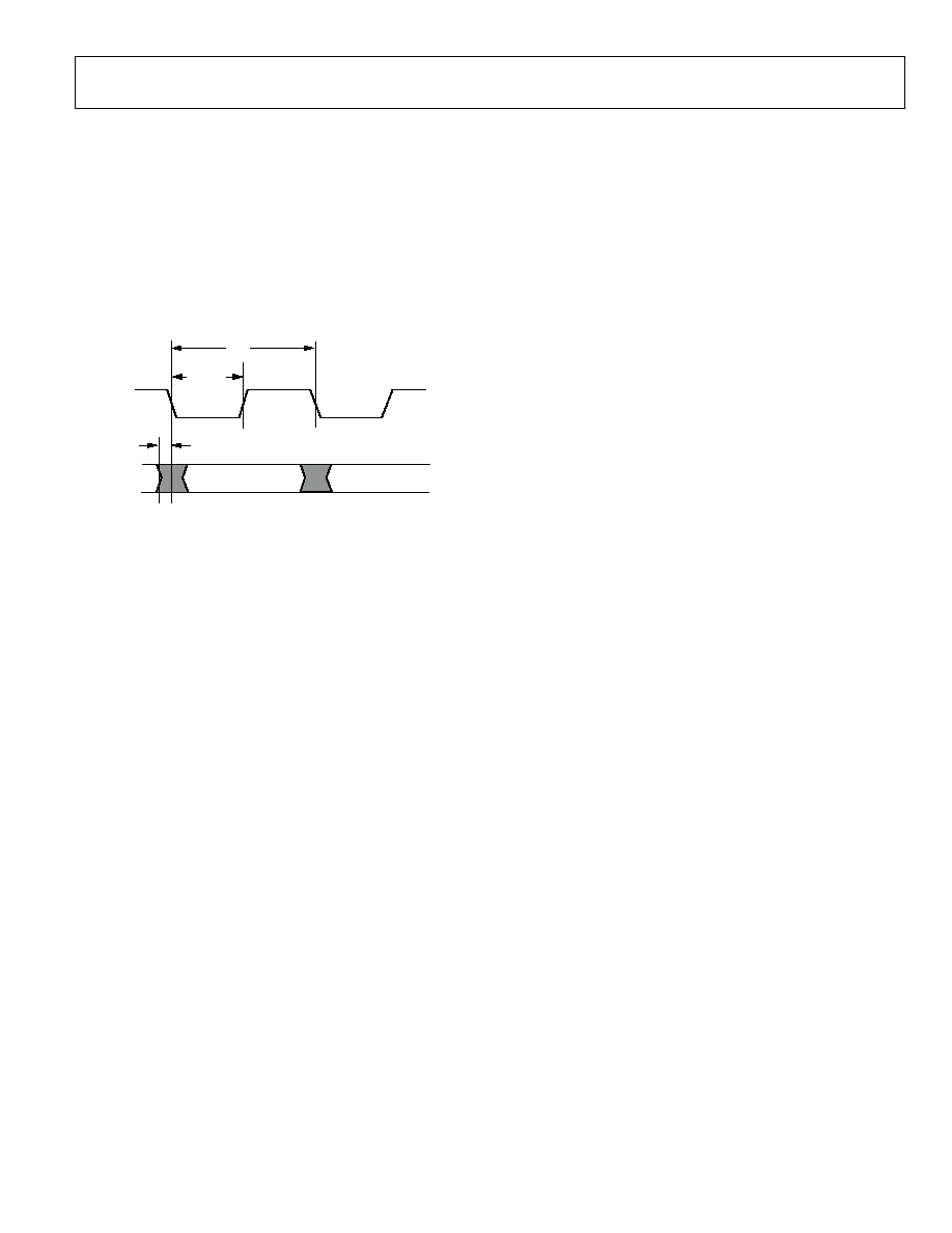
TIMING
The output data clock signal is created so that its rising edge
always occurs between data transitions and can be used to latch
the output data externally.
There is a pipeline in the AD9396, which must be flushed
before valid data becomes available. This means 23 data sets are
presented before valid data is available.
The timing diagram in Figure 7 shows the operation of the
AD9396.
t
PER
t
DCYCLE
t
SKEW
DATACK
05690-009
DATA
HSOUT
Figure 7. Output Timing
HSYNC Timing
Horizontal sync (HSYNC) is processed in the AD9396 to
eliminate ambiguity in the timing of the leading edge with
respect to the phase-delayed pixel clock and data.
The HSYNC input is used as a reference to generate the pixel
sampling clock. The sampling phase can be adjusted, with
respect to HSYNC, through a full 360° in 32 steps via the phase
adjust register (to optimize the pixel sampling time). Display
systems use HSYNC to align memory and display write cycles,
so it is important to have a stable timing relationship between
the HSYNC output (HSOUT) and data clock (DATACK).
Three things happen to HSYNC in the AD9396. First, the
polarity of HSYNC input is determined and thus has a known
output polarity. The known output polarity can be programmed
either active high or active low (Register 0x24, Bit 7). Second,
HSOUT is aligned with DATACK and data outputs. Third, the
duration of HSOUT (in pixel clocks) is set via Register 0x23.
HSOUT is the sync signal that should be used to drive the rest
of the display system.
Coast Timing
In most computer systems, the HSYNC signal is provided con-
tinuously on a dedicated wire. In these systems, the coast input
and function are unnecessary, and should not be used. The pin
should be permanently connected to the inactive state.
In some systems, however, HSYNC is disturbed during the
vertical sync period (VSYNC). In some cases, HSYNC pulses
disappear. In other systems, such as those that employ
composite sync (Csync) signals or embedded SOG, HSYNC
includes equalization pulses or other distortions during
VSYNC. To avoid upsetting the clock generator during VSYNC,
it is important to ignore these distortions. If the pixel clock PLL
sees extraneous pulses, it attempts to lock to this new frequency,
and changes frequency by the end of the VSYNC period. It then
takes a few lines of correct HSYNC timing to recover at the
beginning of a new frame, tearing the image at the top of the
display.
The coast input is provided to eliminate this problem. It is an
asynchronous input that disables the PLL input and allows the
clock to free-run at its then-current frequency. The PLL can
free-run for several lines without significant frequency drift.
Coast can be generated internally by the AD9396 (see
Register 0x12[1]), can be driven directly from a VSYNC input,
or can be provided externally by the graphics controller.
AD9396
Rev. 0 | Page 16 of 48
Sync Processing
The inputs of the sync processing section of the AD9396 are
combinations of digital HSYNCs and VSYNCs, analog sync-on-
green, or sync-on-Y signals, and an optional external coast
signal. From these signals, it generates a precise, jitter-free (9%
or less at 95 MHz) clock from its PLL; an odd/even field signal;
HSYNC and VSYNC out signals; a count of HSYNCs per
VSYNC; and a programmable SOG output. The main sync
processing blocks are the sync slicer, sync separator, HSYNC
filter, HSYNC regenerator, VSYNC filter, and coast generator.
The sync slicer extracts the sync signal from the green graphics
or luminance video signal that is connected to the SOGIN input
and outputs a digital composite sync. The sync separator's task
is to extract VSYNC from the composite sync signal, which can
come from either the sync slicer or the HSYNC input. The
HSYNC filter is used to eliminate any extraneous pulses from
the HSYNC or SOGIN inputs, outputting a clean, low jitter
signal that is appropriate for mode detection and clock
generation. The HSYNC regenerator is used to re-create a clean,
although not low jitter, HSYNC signal that can be used for
mode detection and counting HSYNCs per VSYNC. The
VSYNC filter is used to eliminate spurious VSYNCs, maintain a
stable timing relationship between the VSYNC and HSYNC
output signals, and generate the odd/even field output. The
coast generator creates a robust coast signal that allows the PLL
to maintain its frequency in the absence of HSYNC pulses.
05690-007
AD9396
PLL CLOCK
GENERATOR
HSYNC FILTER
AND
REGENERATOR
HSYNC 0
SOG OUT
HSYNC
COAST
DATACK
SOGIN 0
COAST
CHANNEL
SELECT
VSYNC 1
O/E
FIELD
MUX
MUX
MUX
RH
3
FH
4
SP
5
MUX
1
ACTIVITY DETECT
2
POLARITY DETECT
3
REGENERATED HSYNC
4
FILTERED HSYNC
5
SET POLARITY
SP
5
AD
1
PD
2
PD
2
AD
1
PD
2
AD
1
PD
2
SYNC
SLICER
SYNC
SLICER
VSYNC 0
HSYNC 1
HSYNC OUT
VSYNC OUT
SOGIN 1
HSYNC/VSYNC
COUNTER
REG 26H, 27H
SYNC
PROCESSOR
AND
VSYNC FILTER
MUX
MUX
PLL SYNC FILTER EN
0x21:6
SP SYNC FILTER EN
0x21:7
SOGOUT SELECT
0x24:2,1
[0x11:7]
HSYNC
SELECT
[0x11:3]
COAST SELECT
0x12:1
VSYNC FILTER EN
0x21:5
FILTER COAST VSYNC
0x12:0
VSYNC
VSYNC
FILTERED
VSYNC
AD
1
AD
1
AD
1
SP
5
SP
5
MUX
MUX
MUX
Figure 8. Sync Processing Block Diagram
AD9396
Rev. 0 | Page 17 of 48
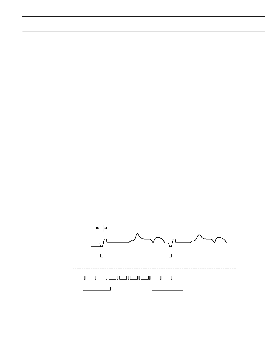
Sync Slicer
The purpose of the sync slicer is to extract the sync signal from
the green graphics or luminance video signal that is connected
to the SOGIN input. The sync signal is extracted in a two-step
process. First, the SOG input (typically 0.3 V below the black
level) is detected and clamped to a known dc voltage. Next, the
signal is routed to a comparator with a variable trigger level (set
by Register 0x1D, Bits [7:3]), but nominally 0.128 V above the
clamped voltage. The sync slicer output is a digital composite
sync signal containing both HSYNC and VSYNC information
(see Figure 9).
Sync Separator
As part of sync processing, the sync separator's task is to extract
VSYNC from the composite sync signal. It works on the idea
that the VSYNC signal stays active for a much longer time than
the HSYNC signal. By using a digital low-pass filter and a
digital comparator, it rejects pulses with small durations (such
as HSYNCs and equalization pulses) and only passes pulses
with large durations, such as VSYNC (see Figure 9).
The threshold of the digital comparator is programmable for
maximum flexibility. To program the threshold duration, write
a value (N) to Register 0x11. The resulting pulse width is
N × 200 ns. So if N = 5, the digital comparator threshold is 1 s.
Any pulses less than 1 s are rejected, while any pulse greater
than 1 s passes through.
The sync separator on the AD9396 is simply an 8-bit digital
counter with a 6 MHz clock. It works independently of the
polarity of the composite sync signal. Polarities are determined
elsewhere on the chip. The basic idea is that the counter counts
up when HSYNC pulses are present. But because HSYNC
pulses are relatively short in width, the counter only reaches a
value of N before the pulse ends. It then starts counting down
until eventually reaching 0 before the next HSYNC pulse
arrives. The specific value of N varies for different video modes,
but is always less than 255. For example, with a 1 s width
HSYNC, the counter only reaches 5 (1 s/200 ns = 5). Now,
when VSYNC is present on the composite sync the counter also
counts up. However, because the VSYNC signal is much longer,
it counts to a higher number, M. For most video modes, M is at
least 255. So VSYNC can be detected on the composite sync
signal by detecting when the counter counts to higher than N.
The specific count that triggers detection, T, can be
programmed through the Serial Register 0x11.
Once VSYNC has been detected, there is a similar process to
detect when it goes inactive. At detection, the counter first
resets to 0, then starts counting up when VSYNC finishes. As in
the previous case, it detects the absence of VSYNC when the
counter reaches the threshold count, T. In this way, it rejects
noise and/or serration pulses. Once VSYNC is detected to be
absent, the counter resets to 0 and begins the cycle again.
There are two things to keep in mind when using the sync
separator. First, the resulting clean VSYNC output is delayed
from the original VSYNC by a duration equal to the digital
comparator threshold (N × 200 ns). Second, there is some
variability to the 200 ns multiplier value. The maximum varia-
bility over all operating conditions is ±20% (160 ns to 240 ns).
Because normal VSYNC and HSYNC pulse widths differ by a
factor of about 500 or more, 20% variability is not an issue.
05690-008
SOGIN
SOGOUT OUTPUT
CONNECTED TO
HSIN
NEGATIVE PULSE WIDTH = 40 SAMPLE CLOCKS
COMPOSITE
SYNC
AT HSIN
VSOUT
FROM SYNC
SEPARATOR
300mV
+300mV
700mV MAXIMUM
0mV
Figure 9. Sync Slicer and Sync Separator Output
AD9396
Rev. 0 | Page 18 of 48
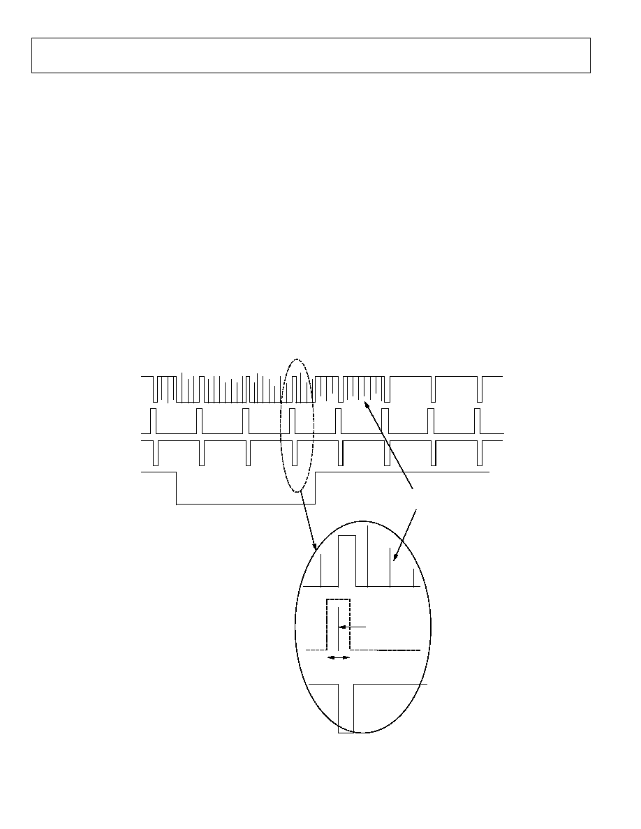
HSYNC Filter and Regenerator
The HSYNC filter is used to eliminate any extraneous pulses
from the HSYNC or SOGIN inputs, outputting a clean, low
jitter signal that is appropriate for mode detection and clock
generation. The HSYNC regenerator is used to re-create a clean,
although not low jitter, HSYNC signal that can be used for
mode detection and counting HSYNCs per VSYNC. The
HSYNC regenerator has a high degree of tolerance to
extraneous and missing pulses on the HSYNC input, but is not
appropriate for use by the PLL in creating the pixel clock
because of jitter.
The HSYNC regenerator runs automatically and requires no
setup to operate. The HSYNC filter requires setting up a filter
window. The filter window sets a periodic window of time
around the regenerated HSYNC leading edge where valid
HSYNCs are allowed to occur. The general idea is that
extraneous pulses on the sync input occur outside of this filter
window and thus are filtered out. To set the filter window
timing, program a value (x) into Register 0x20. The resulting
filter window time is ±x times 25 ns around the regenerated
HSYNC leading edge. Just as for the sync separator threshold
multiplier, allow a ±20% variance in the 25 ns multiplier to
account for all operating conditions (20 ns to 30 ns range).
A second output from the HSYNC filter is a status bit
(Register 0x16[0]) that tells whether extraneous pulses are
present on the incoming sync signal. Extraneous pulses are
often included for copy protection purposes; this status bit can
be used to detect that.
The filtered HSYNC (rather than the raw HSYNC/SOGIN
signal) for pixel clock generation by the PLL is controlled by
Register 0x21[6]. The regenerated HSYNC (rather than the
raw HSYNC/SOGIN signal) for sync processing is controlled by
Register 0x21[7]. Use of the filtered HSYNC and regenerated
HSYNC is recommended. See Figure 10 for an illustration of a
filtered HSYNC.
HSOUT
VSYNC
FILTER
WINDOW
EXPECTED
EDGE
FILTER
WINDOW
EQUALIZATION
PULSES
HSIN
05690-010
Figure 10. Sync Processing Filter
AD9396
Rev. 0 | Page 19 of 48
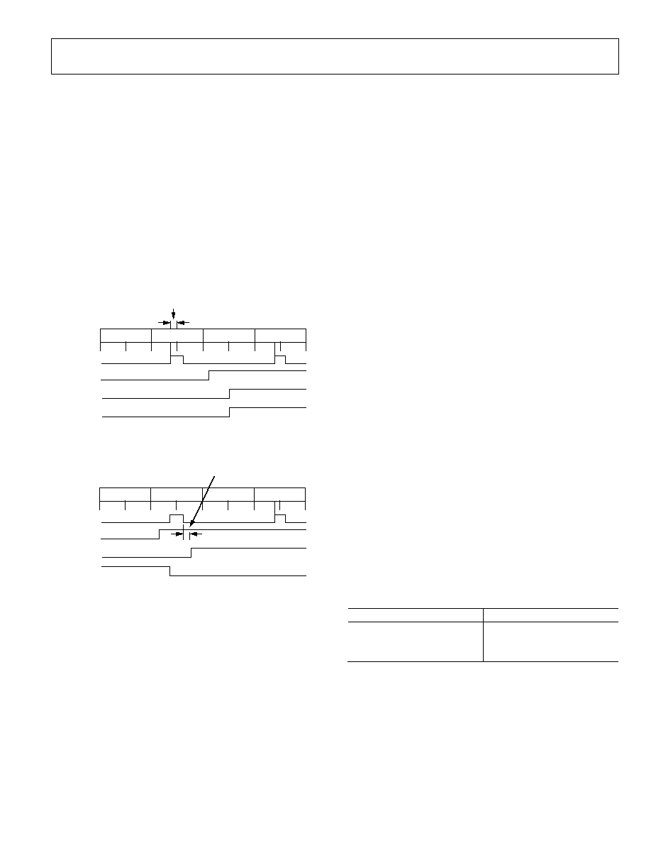
VSYNC Filter and Odd/Even Fields
The VSYNC filter is used to eliminate spurious VSYNCs,
maintain a consistent timing relationship between the VSYNC
and HSYNC output signals, and generate the odd/even field
output.
The filter works by examining the placement of VSYNC with
respect to HSYNC and, if necessary, slightly shifting it in time at
the VSOUT output. The goal is to keep the VSYNC and
HSYNC leading edges from switching at the same time,
eliminating confusion as to when the first line of a frame
occurs. Enabling the VSYNC filter is done with Register
0x21[5]. Use of the VSYNC filter is recommended for all cases,
including interlaced video and is required when using the
HSYNC per VSYNC counter. Figure 12 illustrates even/odd
field determination in two situations.
FIELD 1
FIELD 0
SYNC SEPARATOR THRESHOLD
FIELD 1
FIELD 0
2
3
2
1
4
4
3
1
HSIN
VSIN
VSOUT
O/E FIELD
EVEN FIELD
QUADRANT
05690-011
Figure 11.
FIELD 1
FIELD 0
SYNC SEPARATOR THRESHOLD
FIELD 1
FIELD 0
2
3
2
1
4
3
1
HSIN
VSIN
4
VSOUT
O/E FIELD
ODD FIELD
QUADRANT
05690-012
Figure 12. VSYNC Filter--Odd/Even
DVI RECEIVER
The DVI receiver section of the AD9396 allows the reception of
a digital video stream compatible with DVI 1.0. Embedded in
this data stream are HSYNCs, VSYNCs and display enable (DE)
signals. DVI restricts the received format to RGB, but the
inclusion of a programmable color space converter (CSC)
allows the output to be tailored to any format necessary. With
this, the scaler following the AD9396 can specify that it always
wishes to receive a particular format--for instance, 4:2:2
YCrCb--regardless of the transmitted mode. If RGB is sent, the
CSC can easily convert that to 4:2:2 YCrCb while relieving the
scaler of this task.
DE GENERATOR
The AD9396 has an on-board generator for DE, for start of
active video (SAV), and for end of active video (EAV), all of
which are necessary for describing the complete data stream for
a BT656-compatible output. In addition to this particular
output, it is possible to generate the DE for cases in which a
scaler is not used. This signal alerts the following circuitry as to
which are displayable video pixels.
4:4:4 TO 4:2:2 FILTER
The AD9396 contains a filter that allows it to convert a signal
from YCrCb 4:4:4 to YCrCb 4:2:2 while maintaining the
maximum accuracy and fidelity of the original signal.
Input Color Space to Output Color space
The AD9396 can support a wide variety of output formats, such
as the following:
·
RGB 24-bit
·
4:4:4 YCrCb 8-bit
·
4:2:2 YCrCb 8-bit, 10-bit, and 12-bit
·
Dual 4:2:2 YCrCb 8-bit
Color Space Conversion (CSC) Matrix
The color space conversion (CSC) matrix in the AD9396
consists of three identical processing channels. In each channel,
three input values are multiplied by three separate coefficients.
Also included are an offset value for each row of the matrix and
a scaling multiple for all values. Each value has a 13-bit, twos
complement resolution to ensure the signal integrity is main-
tained. The CSC is designed to run at speeds up to 150 MHz
supporting resolutions up to 1080p at 60 Hz. With any-to-any
color space support, formats such as RGB, YUV, YCbCr, and
others are supported by the CSC.
The main inputs, R
IN
, G
IN
, and B
IN
come from the 8-bit to 12-bit
inputs from each channel. These inputs are based on the input
format detailed in Table 11. The mapping of these inputs to the
CSC inputs is shown in Table 10.
Table 10. CSC Port Mapping
Input Channel
CSC Input Channel
R/CR R
IN
Gr/Y G
IN
B/CB B
B
IN
One of the three channels is represented in Figure 13. In each
processing channel the three inputs are multiplied by three
separate coefficients marked a1, a2, and a3. These coefficients
are divided by 4096 to obtain nominal values ranging from
-0.9998 to +0.9998. The variable labeled `a4' is used as an offset
control. The CSC_Mode setting is the same for all three
processing channels. This multiplies all coefficients and offsets
by a factor of 2
CSC_Mode
.
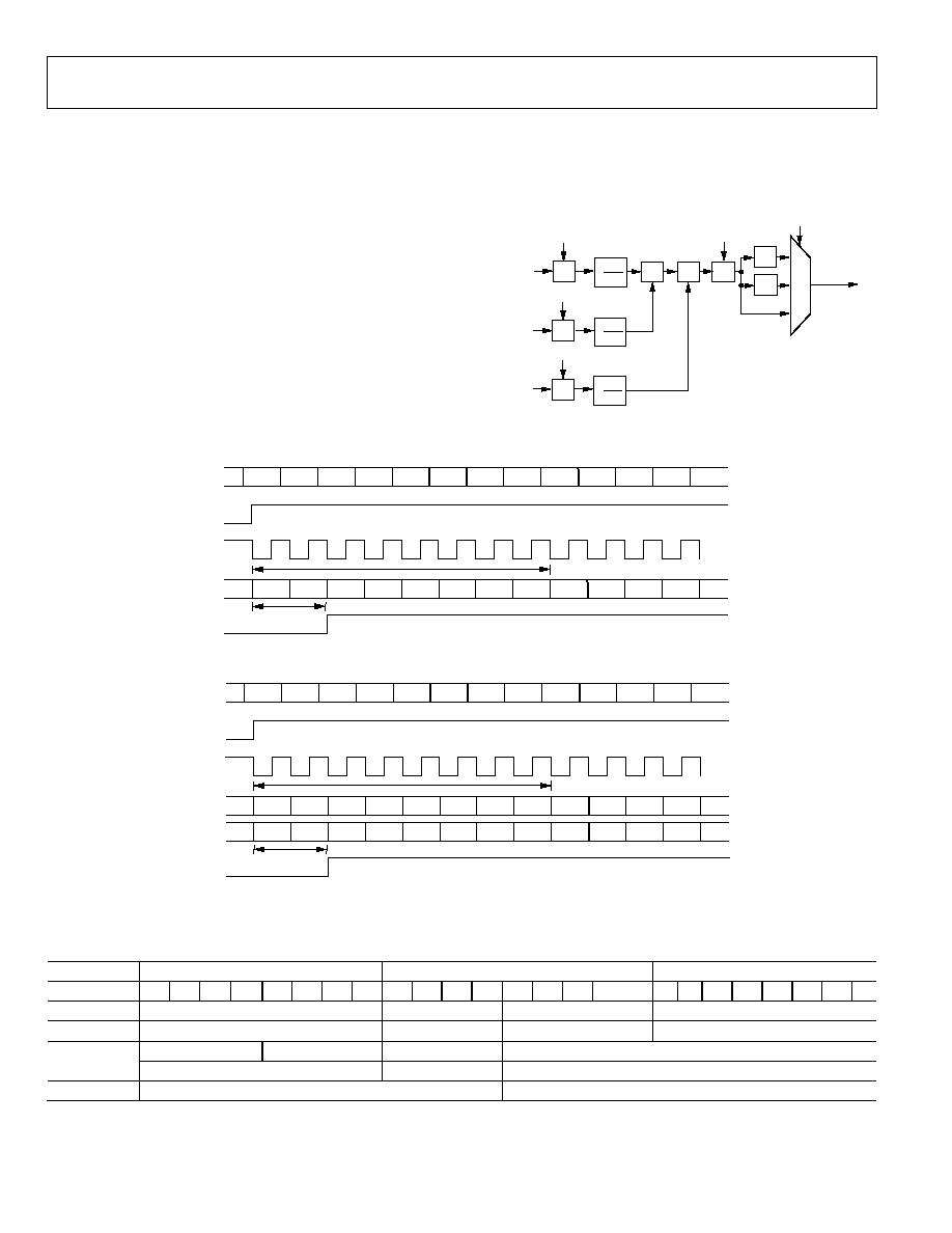
AD9396
Rev. 0 | Page 20 of 48
The functional diagram for a single channel of the CSC, as
shown in Figure 13, is repeated for the remaining G and B
channels. The coefficients for these channels are b1, b2, b3, b4,
c1, c2, c3, and c4.
A programming example and register settings for several
common conversions are listed in the Color Space Converter
(CSC) Common Settings.
For a detailed functional description and more programming
examples, refer to the application note
AN-795, AD9880 Color
Space Converter User's Guide.
TIMING DIAGRAMS
The following timing diagrams show the operation of the
AD9396.The output data clock signal is created so that its rising
edge always occurs between data transitions and can be used to
latch the output data externally. There is a pipeline in the
AD9396, which must be flushed before valid data becomes
available. This means six data sets are presented before valid
data is available.
05690-
013
×2
2
1
0
×
×
×
a1[12:0]
a2[12:0]
a3[12:0]
R
IN
[11:0]
B
IN
[11:0]
G
IN
[11:0]
+
×4
CSC_Mode[1:0]
a4[12:0]
R
OUT
[11:0]
+
1
4096
×
1
4096
×
1
4096
×
+
Figure 13. Single CSC Channel
DATAIN
P0
P1
P2
P5
P3
P4
P9
P6
P8
P10
P11
P7
HSIN
DATACK
8 CLOCK CYCLE DELAYS
DATAOUT
P0
P1
P2
P3
2 CLOCK CYCLE DELAYS
HSOUT
05690-014
Figure 14. RGB ADC Timing
DATAIN
P0
P1
P2
P5
P3
P4
P9
P6
P8
P10
P11
P7
HSIN
DATACK
8 CLOCK CYCLE DELAYS
CB/CROUT
B0
R0
B2
R2
YOUT
Y0
Y1
Y2
Y3
2 CLOCK CYCLE DELAYS
NOTES:
1. PIXEL AFTER HSOUT CORRESPONDS TO BLUE INPUT.
2. EVEN NUMBER OF PIXEL DELAYS BETWEEN HSOUT AND DATAOUT.
HSOUT
05690-015
Figure 15. YCrCb ADC Timing
Table 11.
Port Red
Green
Blue
Bit
7 6 5 4 3 2 1 0 7 6 5 4 3 2 1 0
7 6 5 4 3 2 1 0
4:4:4
Red/Cr [7:0]
Green/Y [7:0]
Blue/Cb [7:0]
4:2:2
CbCr [7:0]
Y [7:0]
DDR 4:2:2
CbCr
Y, Y
DDR
1
G [3:0]
DDR
B [7:4]
DDR
B [3:0]
DDR 4:2:2
CbCr [11:0]
4:4:4 DDR
DDR
R [7:0]
DDR
G [7:4]
DDR 4:2:2
Y,Y [11:0]
4:2:2 to 12
CbCr [11:0]
Y [11:0]
1
Arrows in the table indicate clock edge. Rising edge of clock =
, falling edge = .

AD9396
Rev. 0 | Page 21 of 48
2-WIRE SERIAL REGISTER MAP
The AD9396 is initialized and controlled by a set of registers that determines the operating modes. An external controller is employed to
write and read the control registers through the 2-wire serial interface port.
Table 12. Control Register Map
Hex
Address
Read/Write
or Read Only
Bits
Default
Value
Register Name
Description
0x00
Read
[7:0]
00000000
Chip Revision
Chip revision ID.
0x01
Read/Write
[7:0]
01101001
PLL Divider MSB
PLL feedback divider value MSB.
0x02
Read/Write
[7:4]
1101****
PLL Divider
PLL feedback divider value.
0x03
Read/Write
[7:6]
01******
VCO Range
VCO range.
[5:3]
**001***
Charge Pump
Charge pump current control for PLL.
[2]
*****0**
External Clock
Enable
Selects the external clock input rather than the internal PLL clock.
0x04 Read/Write
[7:3]
10000***
Phase
Adjust Selects the clock phase to use for the ADC clock.
0x05 Read/Write
[7:0]
10000000
Red
Gain
Controls the gain of the red channel PGA. 0 = low gain,
255 = high gain.
0x06 Read/Write
[7:0]
10000000
Green
Gain
Controls the gain of the green channel PGA. 0 = low gain,
255 = high gain.
0x07 Read/Write
[7:0]
10000000
Blue
Gain
Controls the gain of the blue channel PGA. 0 = low gain,
255 = high gain.
0x08
Read/Write
[7:0]
00000000
Red Offset Adjust
User adjustment of auto-offset. Allows user control of brightness.
0x09
Read/Write
[7:0]
10000000
Red Offset
Red offset/target code. 0 = small offset, 255 = large offset.
0x0A Read/Write [7:0]
00000000
Green Offset
Adjust
User adjustment of auto-offset. Allows user control of brightness.
0x0B Read/Write
[7:0]
10000000
Green
Offset Green
offset/target code. 0 = small offset, 255 = large offset.
0x0C
Read/Write
[7:0]
00000000
Blue Offset Adjust
User adjustment of auto-offset. Allows user control of brightness.
0x0D
Read/Write
[7:0]
10000000
Blue Offset
Blue offset/target code. 0 = small offset, 255 = large offset.
0x0E Read/Write
[7:0]
00100000
Sync Separator
Threshold
Selects the maximum HSYNC pulse width for composite sync
separation.
0x0F Read/Write
[7:2]
010000**
SOG Comparator
Threshold Enter
The enter level for the SOG slicer. Must be less than or equal to the
exit level.
0x10 Read/Write
[7:2]
010000**
SOG Comparator
Threshold Exit
The exit level for the SOG slicer. Must be greater than or equal to
the enter level.
0x11
Read/Write
[7]
0*******
HSYNC Source
0 = HSYNC.
1 = SOG.
[6]
*0******
HSYNC Source
Override
0 = auto HSYNC source.
1 = manual HSYNC source.
[5]
**0*****
VSYNC Source
0 = VSYNC.
1 = VSYNC from SOG.
[4]
***0****
VSYNC Source
Override
0 = auto HSYNC source.
1 = manual HSYNC source.
[3]
****0***
Channel Select
0 = Channel 0.
1 = Channel 1.
[2]
*****0**
Channel Select
Override
0 = autochannel select.
1 = manual channel select.
[1]
******0*
Interface Select
0 = analog interface.
1 = digital interface.
[0]
*******0
Interface Override
0 = auto-interface select.
1 = manual interface select.
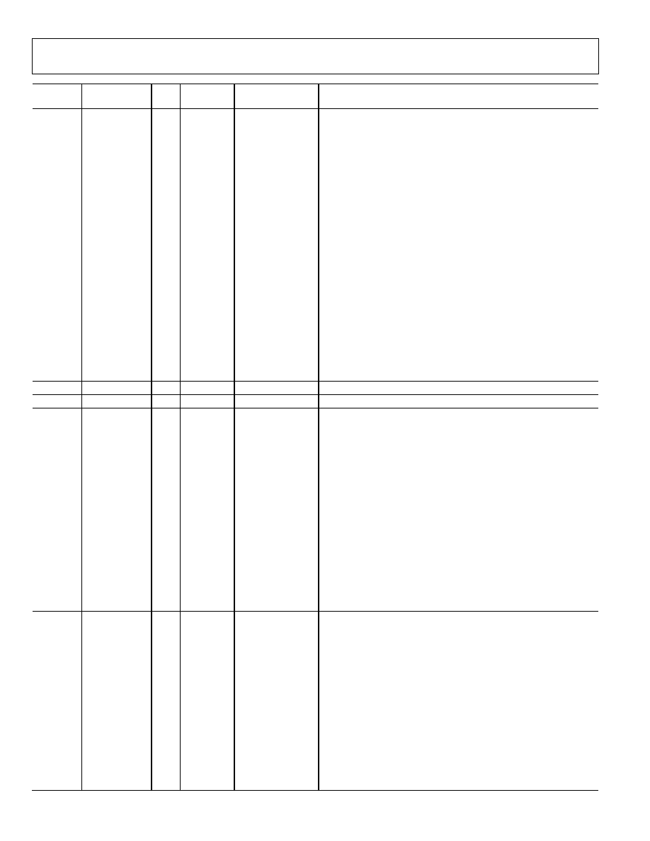
AD9396
Rev. 0 | Page 22 of 48
Hex
Address
Read/Write
or Read Only
Bits
Default
Value Register
Name
Description
0x12 Read/Write
[7]
1*******
Input HSYNC
Polarity
0 = active low.
1 = active high.
[6]
*0******
HSYNC Polarity
Override
0 = auto HSYNC polarity.
1 = manual HSYNC polarity.
[5]
**1*****
Input VSYNC
Polarity
0 = active low.
1 = active high.
[4]
***0****
VSYNC Polarity
Override
0 = auto VSYNC polarity.
1 = manual VSYNC polarity.
[3]
****1***
Input Coast
Polarity
0 = active low.
1 = active high.
[2]
*****0**
Coast Polarity
Override
0 = auto-coast polarity.
1 = manual coast polarity.
[1]
******0*
Coast Source
0 = internal coast.
1 = external coast.
[0]
*******1
Filter Coast VSYNC
0 = Use raw VSYNC for coast generation.
1 = Use filtered VSYNC for coast generation.
0x13
Read/Write
[7:0]
00000000
Precoast
Number of HSYNC periods before VSYNC to coast.
0x14
Read/Write
[7:0]
00000000
Postcoast
Number of HSYNC periods after VSYNC to coast.
0x15 Read
[7]
0*******
HSYNC 0
Detected
0 = not detected.
1 = detected.
[6]
*0******
HSYNC 1
Detected
0 = not detected.
1 = detected.
[5]
**0*****
VSYNC 0 Detected
0 = not detected.
1 = detected.
[4]
***0****
VSYNC 1 Detected
0 = not detected.
1 = detected.
[3]
****0***
SOG 0 Detected
0 = not detected.
1 = detected.
[2]
*****0**
SOG1 Detected
0 = not detected.
1 = detected.
[1]
******0*
Coast Detected
0 = not detected.
1 = detected.
0x16
Read
[7]
0*******
HSYNC 0 Polarity
0 = active low.
1 = active high.
[6]
*0******
HSYNC 1 Polarity
0 = active low.
1 = active high.
[5]
**0*****
VSYNC 0 Polarity
0 = active low.
1 = active high.
[4]
***0****
VSYNC 1 Polarity
0 = active low.
1 = active high.
[3]
****0***
Coast Polarity
0 = active low.
1 = active high.
[2]
*****0**
Pseudo Sync
Detected
0 = not detected.
1 = detected.
[1]
******0*
Sync Filter Locked
0 = not locked.
1 = locked.

AD9396
Rev. 0 | Page 23 of 48
Hex
Address
Read/Write
or Read Only
Bits
Default
Value Register
Name
Description
[0]
*******0
Bad Sync Detect
0 = not detected.
1 = detected.
0x17 Read
[3:0]
****0000
HSYNCs per
VSYNC MSB
MSB of HSYNCs per VSYNC.
0x18 Read
[7:0]
00000000
HSYNCs per
VSYNC
HSYNCs per VSYNC count.
0x19
Read/Write
[7:0]
00001000
Clamp Placement
Number of pixel clocks after trailing edge of HSYNC to begin clamp.
0x1A
Read/Write
[7:0]
00010100
Clamp Duration
Number of pixel clocks to clamp.
0x1B
Read/Write
[7]
0*******
Red Clamp Select
0 = clamp to ground.
1 = clamp to midscale.
[6]
*0******
Green Clamp
Select
0 = clamp to ground.
1 = clamp to midscale.
[5]
**0*****
Blue Clamp Select
0 = clamp to ground.
1 = clamp to midscale.
[4]
***0****
Clamp During
Coast Enable
0 = don't clamp during coast.
1 = clamp during coast.
[3]
****0***
Clamp Disable
0 = internal clamp enabled.
1 = internal clamp disabled.
[1]
******1*
Programmable
Bandwidth
0 = low bandwidth.
1 = full bandwidth.
[0]
*******0
Hold Auto-Offset
0 = normal auto-offset operation.
1 = hold current offset value.
0x1C Read/Write [7]
0*******
Auto-Offset
Enable
0 = manual offset.
1 = auto-offset using offset as target code.
[6:5]
*10*****
Auto-Offset
00 = every clamp.
Update Mode
01 = every 16 clamps.
10 = every 64 clamps.
11 = every VSYNC.
[4:3]
***01***
Difference Shift
00 = 100% of difference used to calculate new offset.
Amount
01 = 50%.
10 = 25%.
11 = 12.5%.
[2]
*****1**
Auto Jump Enable
0 = normal operation.
1 = if code > 15 codes off, offset is jumped to the predicted offset
necessary to fix the >15 code mismatch.
[1]
******1*
Post Filter Enable
0 = disable post filer.
1 = enable post filter.
Post filter reduces update rate by 1/6 and requires that all six
updates recommend a change before changing the offset. This
prevents unwanted offset changes.
[0]
*******0
Toggle Filter
Enable
The toggle filter looks for the offset to toggle back and forth and
holds it if triggered. This prevents toggling in case of missing codes
in the PGA.
0x1D
Read/Write
[7:0]
00001000
Slew Limit
Limits the amount the offset can change by in a single update.
0x1E Read/Write
[7:0]
32
Sync Filter Lock
Threshold
Number of clean HSYNCs required for sync filter to lock.
0x1F Read/Write
[7:0]
50
Sync Filter Unlock
Threshold
Number of missing HSYNCs required to unlock the sync filter. Counter
counts up if HSYNC pulse is missing and down for a good HSYNC.
0x20 Read/Write
[7:0]
50
Sync Filter
Window Width
Width of the window in which HSYNC pulses are allowed.
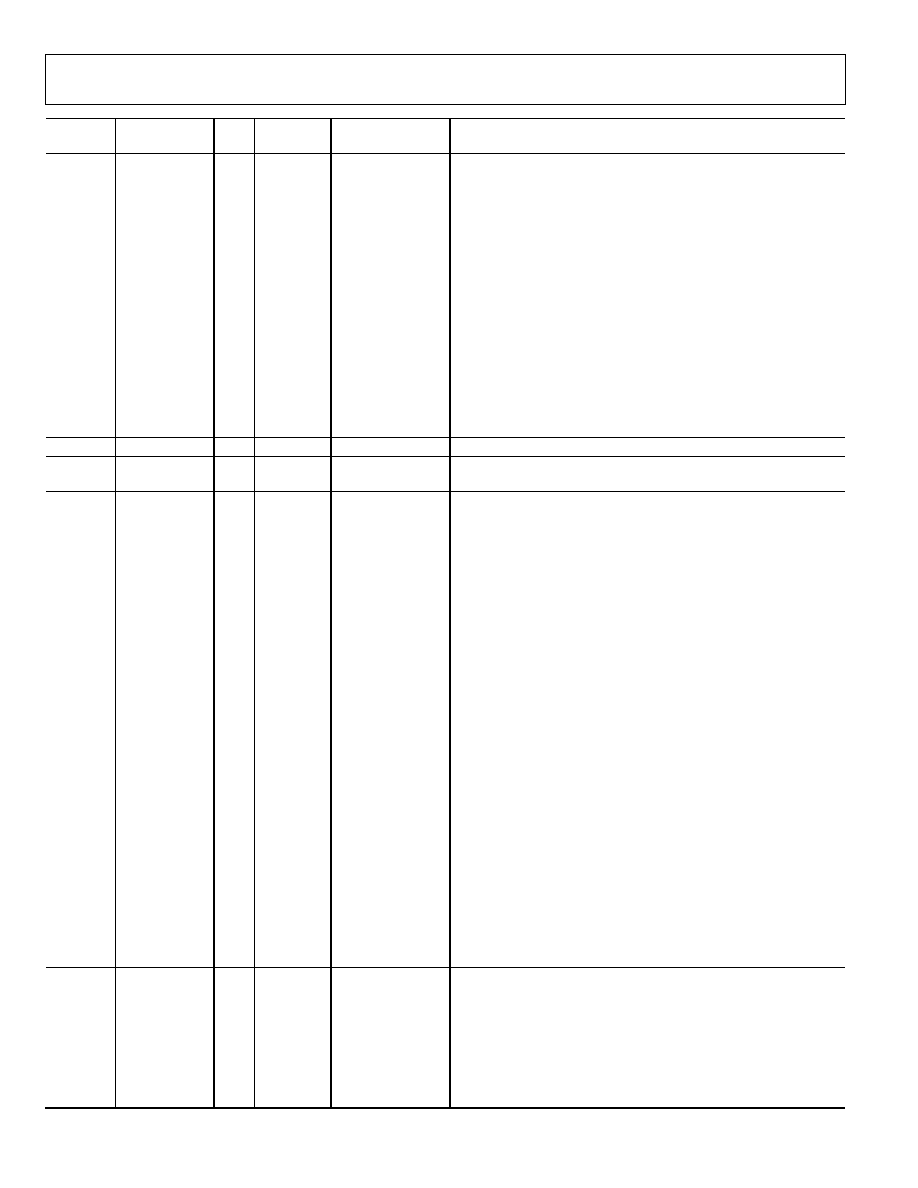
AD9396
Rev. 0 | Page 24 of 48
Hex
Address
Read/Write
or Read Only
Bits
Default
Value Register
Name
Description
0x21 Read/Write
[7]
1*******
SP Sync Filter
Enable
Enables coast, VSYNC duration, and VSYNC filter to use the
regenerated HSYNC rather than the raw HSYNC.
[6]
*1******
PLL Sync Filter
Enable
Enables the PLL to use the filtered HSYNC rather than the raw
HSYNC. This clips any bad HSYNCs, but does not regenerate missing
pulses.
[5]
**0*****
VSYNC Filter
Enable
Enables the VSYNC filter. The VSYNC filter gives a predictable
HSYNC/VSYNC timing relationship but clips one HSYNC period off
the leading edge of VSYNC.
[4]
***0****
VSYNC Duration
Enable
Enables the VSYNC duration block. This block can be used if
necessary to restore the duration of a filtered VSYNC.
[3]
****
1***
Auto-Offset
Clamp Mode
0 = auto-offset measures code during clamp.
1 = auto-offset measures code (10 or 16) clock cycles after end of
clamp for 6 clock cycles.
[2]
****
*1**
Auto-Offset
Clamp Length
Sets delay after end of clamp for auto-offset clamp mode = 1.
0 = delay is 10 clock cycles.
1 = delay is 16 clock cycles.
0x22
Read/Write
[7:0]
4
VSYNC Duration
VSYNC duration.
0x23 Read/Write
[7:0]
32
HSYNC
Duration
HSYNC duration. Sets the duration of the output HSYNC in pixel
clocks.
0x24 Read/Write
[7]
1*******
HSYNC Output
Polarity
Output HSYNC polarity (both DVI and analog). 0 = active low out.
1 = active high out.
[6]
*1******
VSYNC Output
Polarity
Output VSYNC polarity (both DVI and analog).
0 = active low out.
1 = active high out.
[5]
**1*****
DE Output
Polarity
Output DE polarity (both DVI and analog).
0 = active low out.
1 = active high out.
[4]
***1****
Field Output
Polarity
Output field polarity (both DVI and analog).
0 = active low out.
1 = active high out.
[3]
****1***
SOG Output
Polarity
Output SOG polarity (analog only).
0 = active low out.
1 = active high out.
[2:1]
*****11*
SOG Output
Select
Selects signal present on SOG output.
00 = SOG (SOG0 or SOG1).
01 = raw HSYNC (HSYNC0 or HSYNC1).
10 = regenerated sync.
11 = HSYNC to PLL.
[0]
*******0
Output CLK Invert
0 = don't invert clock out.
1 = invert clock out.
0x25
Read/Write
[7:6]
01******
Output CLK Select
Selects which clock to use on output pin. 1× CLK is divided down
from TMDS clock input when pixel repetition is in use.
00 = ½× CLK.
01 = 1× CLK.
10 = 2× CLK.
11 = 90° phase 1× CLK.
[5:4]
**11****
Output Drive
Strength
Sets the drive strength of the outputs.
00 = lowest, 11 = highest.
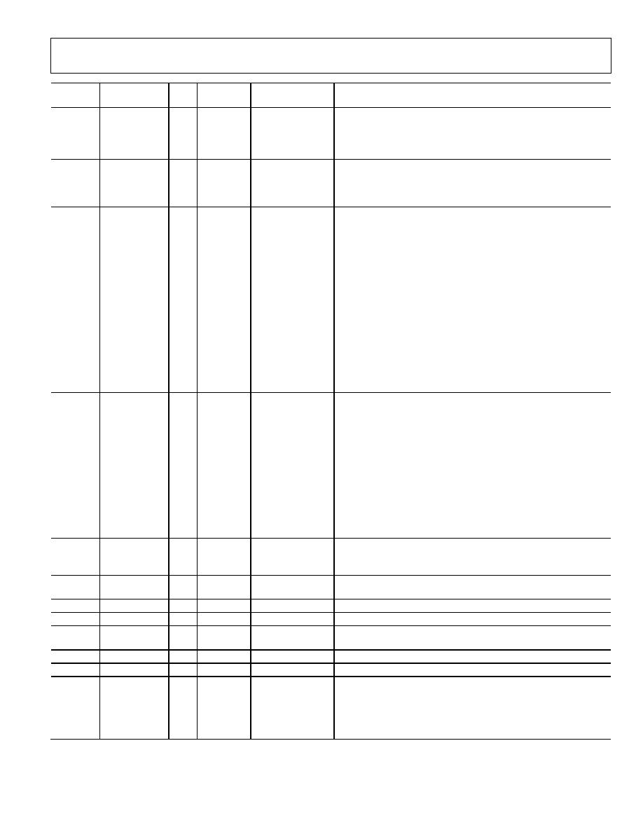
AD9396
Rev. 0 | Page 25 of 48
Hex
Address
Read/Write
or Read Only
Bits
Default
Value Register
Name
Description
[3:2]
****00**
Output Mode
Selects which pins the data comes out on.
00 = 4:4:4 mode (normal).
01 = 4:2:2 + DDR 4:2:2 on blue.
10 = DDR 4:4:4 + DDR 4:2:2 on blue.
[1]
******1*
Primary Output
Enable
Enables primary output.
[0]
*******0
Secondary
Output Enable
Enables secondary output (DDR 4:2:2 in Output Mode 1 and
Mode 2).
0x26 Read/Write
[7]
0*******
Output Three-
State
Three-states the outputs.
[6]
*0******
SOG Three-State
Three-states the SOG output.
[3]
****1***
Power-Down Pin
Polarity
Sets polarity of power-down pin.
0 = active low.
1 = active high.
Selects the function of the power-down pin.
[2:1]
*****00*
Power-Down Pin
Function
00 = power-down.
01 = power-down and three-state SOG.
10 = three-state outputs only.
11 = three-state outputs and SOG.
[0]
*******0
Power-Down
0 = normal.
1 = power-down.
0x27 Read/Write
[7]
1*******
Auto Power-
Down Enable
0 = disable auto low power state.
1 = enable auto low power state.
[6]
*0******
HDCP
A0 Sets the LSB of the address of the HDCP I
2
C. Set to 1 only for a
second receiver in a dual-link configuration.
0 = use internally generated MCLK.
1 = use external MCLK input.
[4]
***0****
BT656 EN
Enables EAV/SAV codes to be inserted into the video output data.
[3]
****0***
Force DE
Generation
Allows use of the internal DE generator in DVI mode.
[2:0]
*****000
Interlace
Offset
Sets the difference (in HSYNCs) in field length between Field 0 and
Field 1.
0x28 Read/Write
[7:2]
011000**
VS
Delay
Sets the delay (in lines) from VSYNC leading edge to the start of
active video.
[1:0]
******01
HS Delay MSB
MSB, Register 0x29.
0x29 Read/Write
[7:0]
00000100
HS
Delay
Sets the delay (in pixels) from HSYNC leading edge to the start of
active video.
0x2A
Read/Write
[3:0]
****0101
Line Width MSB
MSB, Register 0x2B.
0x2B
Read/Write
[7:0]
00000000
Line Width
Sets the width of the active video line (in pixels).
0x2C Read/Write [3:0]
****0010
Screen Height
MSB
MSB, Register 0x2D.
0x2D
Read/Write
[7:0]
11010000
Screen Height
Sets the height of the active screen (in lines).
0x2E
Read/Write
[7]
0*******
Test 1
Must be written to 1 for proper operation.
0x2F Read
[6]
*0******
TMDS Sync
Detect
Detects a TMDS DE.
[5]
**0*****
TMDS Active
Detects a TMDS clock.
[3]
****0***
HDCP Keys Read
Returns 1 when read of EEPROM keys is successful.
[2:0]
*****000
DVI Quality
Returns quality number based on DE edges.

AD9396
Rev. 0 | Page 26 of 48
Hex
Address
Read/Write
or Read Only
Bits
Default
Value Register
Name
Description
0x30 Read
[6]
*0******
DVI Content
Encrypted
This bit is high when HDCP decryption is in use (content is
protected). The signal goes low when HDCP is not being used.
Customers can use this bit to determine whether to allow copying
of the content. The bit should be sampled at regular intervals
because it can change on a frame by frame basis.
[5]
**0*****
DVI HSYNC
Polarity
Returns DVI HSYNC polarity.
[4]
***0****
DVI VSYNC
Polarity
Returns DVI VSYNC polarity.
0x31
Read/Write
[7:4]
1001****
MV Pulse Max
Sets the maximum pseudo sync pulse width for Macrovision
detection.
[3:0]
****0110
MV Pulse Min
Sets the minimum pseudo sync pulse width for Macrovision
detection.
0x32 Read/Write
[7]
0*******
MV Oversample
En
Tells the Macrovision detection engine whether oversampling is in
use.
[6]
*0******
MV Pal En
Tells the Macrovision detection engine to enter PAL mode.
[5:0]
**001101
MV Line Count
Start
Sets the start line for Macrovision detection.
0x33
Read/Write
[7]
1*******
MV Detect Mode
0 = standard definition.
1 = progressive scan mode.
[6]
*0******
MV Settings
Override
0 = use hard coded settings for line counts and pulse widths.
1 = use I
2
C values for these settings.
[5:0]
**010101
MV Line Count
End
Sets the end line for Macrovision detection.
0x34 Read/Write
[7:6]
10******
MV Pulse Limit
Set
Sets the number of pulses required in the last 3 lines (SD mode
only).
[5]
**0*****
Low Freq Mode
Sets whether the Audio PLL is in low frequency mode. Low
frequency mode should only be set for pixel clocks <80 MHz.
[4]
***0****
Low Freq
Override
Allows the previous bit to be used to set low frequency mode
rather than the internal auto-detect.
[3]
****0***
Up Conversion
Mode
0 = repeat Cr and Cb values.
1 = interpolate Cr and Cb values.
[2]
*****0**
CrCb Filter Enable
Enables the FIR filter for 4:2:2 CrCb output.
[1]
******0*
CSC_Enable
Enables the color space converter (CSC). The default settings for the
CSC provide HDTV-to-RGB conversion.
Sets the fixed point position of the CSC coefficients, including the
A4, B4, and C4 offsets.
0x35
Read/Write
[6:5]
*01* ****
CSC_Mode
00 = ±1.0, -4096 to +4095.
01 = ±2.0, -8192 to +8190.
1× = ±4.0, -16384 to +16380.
[4:0]
***01100
CSC_Coeff_A1
MSB
MSB, Register 0x36.
0x36
Read/Write
[7:0]
01010010
CSC_Coeff_A1
Color space converter (CSC) coefficient for equation:
R
OUT
= (A1 × R
IN
) + (A2 × G
IN
) + (A3 × B
IN
) + A4
G
OUT
= (B1 × R
IN
) + (B2 × G
IN
) + (B3 × B
IN
) + B4
B
B
OUT
= (C1 × R
IN
) + (C2 × G
IN
) + (C3 × B
IN
) + C4
0x37 Read/Write
[4:0]
***01000
CSC_Coeff_A2
MSB
MSB, Register 0x38.
0x38
Read/Write
[7:0]
00000000
CSC_Coeff_A2 LSB
CSC coefficient for equation:
R
OUT
= (A1 × R
IN
+ (A2 × G
IN
) + (A3 × B
IN
) + A4
G
OUT
= (B1 × R
IN
) + (B2 × G
IN
) + (B3 × B
IN
) + B4
B
B
OUT
= (C1 × R
IN
) + (C2 × G
IN
) + (C3 × B
IN
) + C4
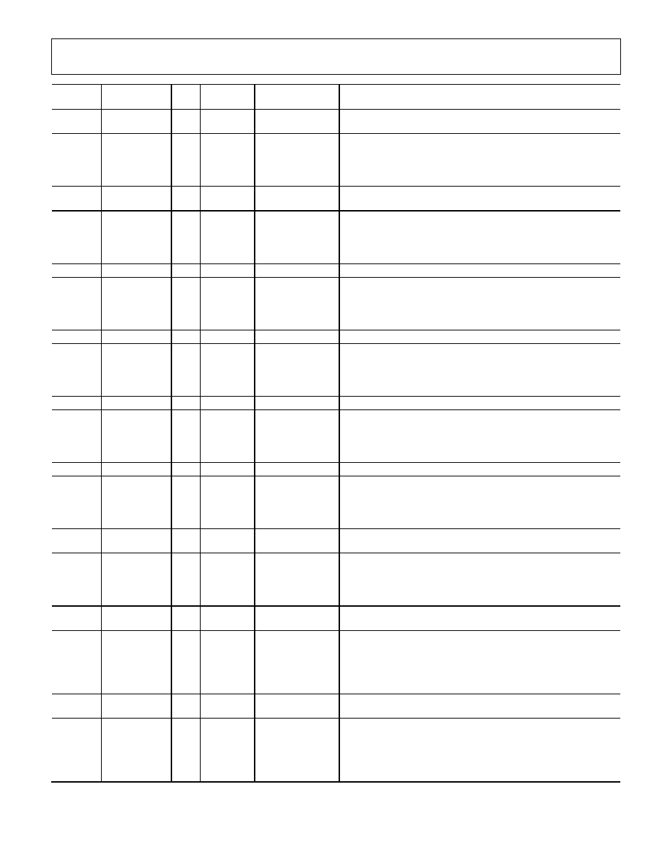
AD9396
Rev. 0 | Page 27 of 48
Hex
Address
Read/Write
or Read Only
Bits
Default
Value Register
Name
Description
0x39 Read/Write
[4:0]
***00000
CSC_Coeff_A3
MSB
MSB, Register 0x3A.
0x3A
Read/Write
[7:0]
00000000
CSC_Coeff_A3 LSB
CSC coefficient for equation:
R
OUT
= (A1 × R
IN
) + (A2 × G
IN
) + (A3 × B
IN
) + A4
G
OUT
= (B1 × R
IN
) + (B2 × G
IN
) + (B3 × B
IN
) + B4
B
B
OUT
= (C1 × R
IN
) + (C2 × G
IN
) + (C3 × B
IN
) + C4
0x3B Read/Write
[4:0]
***11001
CSC_Coeff_A4
MSB
MSB, Register 0x3C.
0x3C
Read/Write
[7:0]
11010111
CSC_Coeff_A4 LSB
CSC coefficient for equation:
R
OUT
= (A1 × R
IN
) + (A2 × G
IN
) + (A3 × B
IN
) + A4
G
OUT
= (B1 × R
IN
) + (B2 × G
IN
) + (B3 × B
IN
) + B4
B
B
OUT
= (C1 × R
IN
) + (C2 × G
IN
) + (C3 × B
IN
) + C4
0x3D
Read/Write
[4:0]
***11100
CSC_Coeff_B1 MSB
MSB, Register 0x3E.
0x3E
Read/Write
[7:0]
01010100
CSC_Coeff_B1 LSB
CSC coefficient for equation:
R
OUT
= (A1 × R
IN
) + (A2 × G
IN
) + (A3 × B
IN
) + A4
G
OUT
= (B1 × R
IN
) + (B2 × G
IN
) + (B3 × B
IN
) + B4
B
B
OUT
= (C1 × R
IN
) + (C2 × G
IN
) + (C3 × B
IN
) + C4
0x3F
Read/Write
[4:0]
***01000
CSC_Coeff_B2 MSB
MSB, Register 0x40.
0x40
Read/Write
[7:0]
00000000
CSC_Coeff_B2 LSB
CSC coefficient for equation:
R
OUT
= (A1 × R
IN
) + (A2 × G
IN
) + (A3 × B
IN
) + A4
G
OUT
= (B1 × R
IN
) + (B2 × G
IN
) + (B3 × B
IN
) + B4
B
B
OUT
= (C1 × R
IN
) + (C2 × G
IN
) + (C3 × B
IN
) + C4
0x41
Read/Write
[4:0]
***11110
CSC_Coeff_B3 MSB
MSB, Register 0x42.
0x42
Read/Write
[7:0]
10001001
CSC_Coeff_B3 LSB
CSC coefficient for equation:
R
OUT
= (A1 × R
IN
+ (A2 × G
IN
) + (A3 × B
IN
) + A4
G
OUT
= (B1 × R
IN
) + (B2 × G
IN
) + (B3 × B
IN
) + B4
B
B
OUT
= (C1 × R
IN
) + (C2 × G
IN
) + (C3 × B
IN
) + C4
0x43
Read/Write
[4:0]
***00010
CSC_Coeff_B4 MSB
MSB, Register 0x44.
0x44
Read/Write
[7:0]
10010010
CSC_Coeff_B4 LSB
CSC coefficient for equation:
R
OUT
= (A1 × R
IN
) + (A2 × R
IN
) + (A3 × B
IN
) + A4
G
OUT
= (B1 × R
IN
) + (B2 × G
IN
) + (B3 × B
IN
) + B4
B
B
OUT
= (C1 × R
IN
) + (C2 × G
IN
) + (C3 × B
IN
) + C4
0x45 Read/Write
[4:0]
***00000
CSC_Coeff_C1
MSB
MSB, Register 0x46.
0x46
Read/Write
[7:0]
00000000
CSC_Coeff_C1 LSB
CSC coefficient for equation:
R
OUT
= (A1 × R
IN
) + (A2 × G
IN
) + (A3 × B
IN
) + A4
G
OUT
= (B1 × R
IN
) + (B2 × G
IN
) + (B3 × B
IN
) + B4
B
B
OUT
= (C1 × R
IN
) + (C2 × G
IN
) + (C3 × B
IN
) + C4
0x47 Read/Write
[4:0]
***01000
CSC_Coeff_C2
MSB
MSB, Register 0x48.
0x48 Read/Write
[7:0]
00000000
CSC_Coeff_C2
LSB
CSC coefficient for equation:
R
OUT
= (A1 × R
IN
) + (A2 × G
IN
) + (A3 × B
IN
) + A4
G
OUT
= (B1 × R
IN
) + (B2 × G
IN
) + (B3 × B
IN
) + B4
B
B
OUT
= (C1 × R
IN
) + (C2 × G
IN
) + (C3 × B
IN
) + C4
0x49 Read/Write
[4:0]
***01110
CSC_Coeff_C3
MSB
MSB, Register 0x4A.
0x4A Read/Write [7:0]
10000111
CSC_Coeff_C3
LSB
CSC coefficient for equation:
R
OUT
= (A1 × R
IN
) + (A2 × G
IN
) + (A3 × B
IN
) + A4
G
OUT
= (B1 × R
IN
) + (B2 × G
IN
) + (B3 × B
IN
) + B4
B
B
OUT
= (C1 × R
IN
) + (C2 × G
IN
) + (C3 × B
IN
) + C4
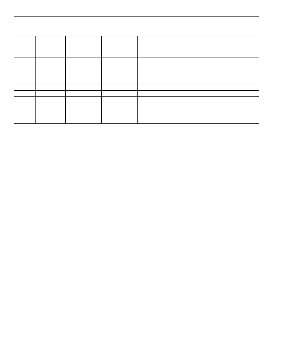
AD9396
Rev. 0 | Page 28 of 48
Hex
Address
Read/Write
or Read Only
Bits
Default
Value Register
Name
Description
0x4B Read/Write
[4:0]
***11000
CSC_Coeff_C4
MSB
MSB, Register 0x4C.
0x4C Read/Write [7:0]
10111101
CSC_Coeff_C4
LSB
CSC coefficient for equation:
R
OUT
= (A1 × R
IN
) + (A2 × G
IN
) + (A3 × B
IN
) + A4
G
OUT
= (B1 × R
IN
) + (B2 × G
IN
) + (B3 × B
IN
) + B4
B
B
OUT
= (C1 × R
IN
) + (C2 × G
IN
) + (C3 × B
IN
) + C4
0x50
Read/Write
[7:0]
00100000
Must be written to 0x20 for proper operation.
0x56
Read/Write
[7:0]
00001111
Must be written to default 0x0F for proper operation.
0x59
Read/Write
[6]
MDA/MCL PU
This disables the MDA/MCL pull-ups.
[5]
CLK Term O/R
Clock termination power-down override: 0 = auto, 1 = manual.
[4]
Manual CLK Term
Clock termination: 0 = normal, 1 = disconnected.
[0]
MDA/MCL Three-
State
This bit three-states the MDA/MCL lines.
AD9396
Rev. 0 | Page 29 of 48
2-WIRE SERIAL CONTROL REGISTER DETAILS
CHIP IDENTIFICATION
0x00--Bits[7:0] Chip Revision
An 8-bit value that reflects the current chip revision.
PLL DIVIDER CONTROL
0x01--Bits[7:0] PLL Divide Ratio MSBs
The eight most significant bits of the 12-bit PLL divide ratio
PLLDIV.
The PLL derives a pixel clock from the incoming HSYNC
signal. The pixel clock frequency is then divided by an integer
value such that the output is phase locked to HSYNC. This
PLLDIV value determines the number of pixel times (pixels
plus horizontal blanking overhead) per line. This is typically
20% to 30% more than the number of active pixels in the
display.
The 12-bit value of the PLL divider supports divide ratios from
221 to 4095. The higher the value loaded in this register, the
higher the resulting clock frequency with respect to a fixed
HSYNC frequency.
VESA has established some standard timing specifications,
which assists in determining the value for PLLDIV as a function
of horizontal and vertical display resolution and frame rate
(see Table 9).
However, many computer systems do not conform precisely to
the recommendations, and these numbers should be used only
as a guide. The display system manufacturer should provide
automatic or manual means for optimizing PLLDIV. An
incorrectly set PLLDIV usually produces one or more vertical
noise bars on the display. The greater the error, the greater the
number of bars produced.
The power-up default value of PLLDIV is 1693 (PLLDIVM =
0x69, PLLDIVL = 0xDx).
The AD9396 updates the full divide ratio only when the LSBs
are changed. Writing to this register by itself does not trigger an
update.
0x02--Bits[7:4] PLL Divide Ratio LSBs
The four least significant bits of the 12-bit PLL divide ratio
PLLDIV.
The power-up default value of PLLDIV is 1693 (PLLDIVM =
0x69, PLLDIVL = 0xDx).
CLOCK GENERATOR CONTROL
0x03--Bits[7:6] VCO Range Select
Two bits that establish the operating range of the clock
generator. VCORNGE must be set to correspond with the
desired operating frequency (incoming pixel rate). The PLL
gives the best jitter performance at high frequencies. For this
reason, to output low pixel rates and still get good jitter
performance, the PLL actually operates at a higher frequency
but then divides down the clock rate. Table 13 shows the pixel
rates for each VCO range setting. The PLL output divisor is
automatically selected with the VCO range setting.
Table 13. VCO Ranges
VCO Range
Pixel Rate Range
00
12 to 30
01
30 to 60
10
60 to 120
11
120 to 150
The power-up default value is 01.
Bits[5:3] Charge Pump Current
Three bits that establish the current driving the loop filter in the
clock generator.
Table 14. Charge Pump Currents
Ip2 Ip1 Ip0 Current
(A)
0 0 0 50
0 0 1 100
0 1 0 150
0 1 1 250
1 0 0 350
1 0 1 500
1 1 0 750
1 1 1 1500
The power-up default value is current = 001.
Bit[2] External Clock Enable
This bit determines the source of the pixel clock.
A Logic 0 enables the internal PLL that generates the pixel clock
from an externally provided HSYNC.
A Logic 1 enables the external CKEXT input pin. In this mode,
the PLL divide ratio (PLLDIV) is ignored. The clock phase
adjusts (phase is still functional). The power-up default value is
EXTCLK = 0.
0x04--Bits[7:3] Phase Adjust
These bits provide a phase adjustment for the DLL to generate
the ADC clock, a 5-bit value that adjusts the sampling phase in
32 steps across one pixel time. Each step represents an 11.25°
shift in sampling phase. The power-up default is 16.

AD9396
Rev. 0 | Page 30 of 48
INPUT GAIN
0x05--Bits[7:0] Red Channel Gain
These bits control the programmable gain amplifier (PGA) of
the red channel. The AD9396 can accommodate input signals
with a full-scale range of between 0.5 V p-p and 1.0 V p-p.
Setting the red gain to 255 corresponds to an input range of
1.0 V. A red gain of 0 establishes an input range of 0.5 V. Note
that increasing red gain results in the picture having less
contrast (the input signal uses fewer of the available converter
codes). The power-up default is 0x80.
0x06--Bits[7:0] Green Channel Gain
These bits control the PGA of the green channel. The AD9396
can accommodate input signals with a full-scale range of
between 0.5 V p-p and 1.0 V p-p. Setting the green gain to
255 corresponds to an input range of 1.0 V. A green gain of
0 establishes an input range of 0.5 V. Note that increasing green
gain results in the picture having less contrast (the input signal
uses fewer of the available converter codes). The power-up
default is 0x80.
0x07--Bits[7:0] Blue Channel Gain
These bits control the PGA of the blue channel. The AD9396
can accommodate input signals with a full-scale range of
between 0.5 V and 1.0 V p-p. Setting the blue gain to 255
corresponds to an input range of 1.0 V. A blue gain of 0
establishes an input range of 0.5 V. Note that increasing blue
gain results in the picture having less contrast (the input signal
uses fewer of the available converter codes). The power-up
default is 0x80.
INPUT OFFSET
0x08--Bits[7:0] Red Channel Offset Adjust
If clamp feedback is enabled, the 8-bit offset adjust determines
the clamp code. The 8-bit offset adjust is a twos complement
number consisting of 1 sign bit plus 7 bits (0x7F = +127, 0x00 =
0, 0xFF = -1, and 0x80 = -128). For example, if the register is
programmed to 130d, then the output code is equal to 130d at
the end of the clamp period. Note that incrementing the offset
register setting by 1 LSB adds 1 LSB of offset, regardless of the
clamp feedback setting. The power-up default is 0.
0x09--Bits[7:0] Red Channel Offset
These eight bits are the red channel offset control. The offset
control shifts the analog input, resulting in a change in bright-
ness. Note that the function of the offset register depends on
whether clamp feedback is enabled (Register 0x1C, Bit 7 = 1).
If clamp feedback is disabled, the offset register bits control the
absolute offset added to the channel. The offset control provides
+127/-128 LSBs of adjustment range, with 1 LSB of offset
corresponding to 1 LSB of output code. If clamp feedback is
enabled these bits provide the relative offset (brightness) from
the offset adjust in the previous register. The power-up default
is 0x80.
0x0A--Bits[7:0] Green Channel Offset Adjust
If clamp feedback is enabled, the 8-bit offset adjust determines
the clamp code. The 8-bit offset adjust is a twos complement
number consisting of 1 sign bit plus 7 bits (0x7F = +127, 0x00 =
0, 0xFF = -1, and 0x80 = -128). For example, if the register is
programmed to 130d, then the output code is equal to 130d at
the end of the clamp period. Note that incrementing the offset
register setting by 1 LSB adds 1 LSB of offset, regardless of the
clamp feedback setting. The power-up default is 0.
0x0B--Bits[7:0] Green Channel Offset
These eight bits are the green channel offset control. The offset
control shifts the analog input, resulting in a change in bright-
ness. Note that the function of the offset register depends on
whether clamp feedback is enabled (Register 0x1C, Bit 7 = 1).
If clamp feedback is disabled, the offset register bits control the
absolute offset added to the channel. The offset control provides
an adjustment range of +127/-128 LSBs, with one LSB of offset
corresponding to 1 LSB of output code. If clamp feedback is
enabled, these bits provide the relative offset (brightness) from
the offset adjust in the previous register. The power-up default
is 0x80.
0x0C--Bits[7:0] Blue Channel Offset Adjust
If clamp feedback is enabled, the 8-bit offset adjust determines
the clamp code. The 8-bit offset adjust is a twos complement
number consisting of 1 sign bit plus 7 bits (0x7F = +127, 0x00 =
0, 0xFF = -1, and 0x80 = -128). For example, if the register is
programmed to 130d, then the output code is equal to 130d at
the end of the clamp period. Note that incrementing the offset
register setting by 1 LSB adds 1 LSB of offset, regardless of the
clamp feedback setting. The power-up default is 0.
0x0D--Bits[7:0] Blue Channel Offset
These eight bits are the blue channel offset control. The offset
control shifts the analog input, resulting in a change in bright-
ness. Note that the function of the offset register depends on
whether clamp feedback is enabled (Register 0x1C, Bit 7 = 1).
If clamp feedback is disabled, the offset register bits control the
absolute offset added to the channel. The offset control provides
an adjustment range of +127/-128 LSBs, with 1 LSB of offset
corresponding to 1 LSB of output code. If clamp feedback is
enabled, these bits provide the relative offset (brightness) from
the offset adjust in the previous register. The power-up default
is 0x80.
SYNC
0x0E--Bits[7:0] Sync Separator
Selects the maximum HSYNC pulse width for composite sync
separation. Power-down default is 0x20.
0x0F--Bits[7:2] SOG Comparator Threshold Enter
The enter level for the SOG slicer. Must be < the exit level
(Register 0x10). The power-up default is 0x10.

AD9396
Rev. 0 | Page 31 of 48
0x10--Bits[7:2] SOG Comparator Threshold Exit
The exit level for the SOG slicer. Must be > the enter level
(Register 0x0F). The power-up default is 0x10.
0x11--Bit[7] HSYNC Source
0 = HSYNC, 1 = SOG. The power-up default is 0. These
selections are ignored if Register 0x11, Bit 6 = 0.
0x11--Bit[6] HSYNC Source Override
0 = auto HSYNC source, 1 = manual HSYNC source. Manual
HSYNC source is defined in Register 0x11, Bit 7. The power-up
default is 0.
0x11--Bit[5] VSYNC Source
0 = VSYNC, 1 = VSYNC from SOG. The power-up default is 0.
These selections are ignored if Register 0x11, Bit 4 = 0.
0x11--Bit[4] VSYNC Source Override
0 = auto VSYNC source, 1 = manual VSYNC source. Manual
VSYNC source is defined in Register 0x11, Bit 5. The power-up
default is 0.
0x11--Bit[3] Channel Select
0 = Channel 0, 1 = Channel 1. The power-up default is 0. These
selections are ignored if Register 0x11, Bit 2 = 0.
0x11--Bit[2] Channel Select Override
0 = auto channel select, 1 = manual channel select. Manual
channel select is defined in Register 0x11, Bit 3. The power-up
default is 0.
0x11--Bit[1] Interface Select
0 = analog interface, 1 = digital interface. The power-up default
is 0. These selections are ignored if Register 0x11, Bit 0 = 0.
0x11--Bit[0] Interface Select Override
0 = auto interface select, 1 = manual interface select. Manual
interface select is defined in Register 0x11, Bit 1. The power-up
default is 0.
0x12--Bit[7] Input HSYNC Polarity
0 = active low, 1 = active high. The power-up default is 1. These
selections are ignored if Register 10x2, Bit 6 = 0.
0x12--Bit[6] HSYNC Polarity Override
0 = auto HSYNC polarity, 1 = manual HSYNC polarity. Manual
HSYNC polarity is defined in Register 0x11,
Bit 7. The power-up default is 0.
0x12--Bit[5] Input VSYNC Polarity
0 = active low, 1 = active high. The power-up default is 1. These
selections are ignored if Register 0x11,Bit 4 = 0.
0x12--Bit[4] VSYNC Polarity Override
0 = auto VSYNC polarity, 1 = manual VSYNC polarity. Manual
VSYNC polarity is defined in Register 0x11, Bit 5. The power-
up default is 0.
COAST AND CLAMP CONTROLS
0x12--Bit[3] Input Coast Polarity
0 = active low, 1 = active high. The power-up default
is 1.
0x12--Bit[2] Coast Polarity Override
0 = auto-coast polarity, 1 = manual coast polarity. The power-
up default is 0.
0x12--Bit[1] Coast Source
0 = internal coast, 1 = external coast. The power-up default is 0.
0x12--Bit[0] Filter Coast VSYNC
0 = use raw VSYNC for coast generation, 1 = use filtered
VSYNC for coast generation The power-up default is 1.
0x13--Bits[7:0] Precoast
This register allows the internally generated coast signal to be
applied prior to the VSYNC signal. This is necessary in cases
where pre-equalization pulses are present. The step size for this
control is one HSYNC period. For precoast to work correctly, it
is necessary for the VSYNC filter (0x21, Bit 5) and sync
processing filter (0x21 Bit 7) both to be either enabled or
disabled. The power-up default is 0.
0x14--Bits[7:0] Postcoast
This register allows the internally generated coast signal to be
applied following the VSYNC signal. This is necessary in cases
where postequalization pulses are present. The step size for this
control is one HSYNC period. For postcoast to work correctly,
it is necessary for the VSYNC filter (0x21, Bit 5) and sync
processing filter (0x21, Bit 7) both to be either enabled or
disabled. The power-up default is 0.
STATUS OF DETECTED SIGNALS
0x15--Bit[7] HSYNC0 Detection Bit
Indicates if HSYNC0 is active. This bit is used to indicate when
activity is detected on the HSYNC0 input pin. If HSYNC is held
high or low, activity is not detected. The sync processing block
diagram shows where this function is implemented. 0 =
HSYNC0 not active. 1 = HSYNC0 is active.
0x15--Bit[6] HSYNC1 Detection Bit
Indicates if HSYNC1 is active. This bit is used to indicate when
activity is detected on the HSYNC1 input pin. If HSYNC is held
high or low, activity is not detected. The sync processing block
diagram shows where this function is implemented. 0 =
HSYNC1 not active. 1 = HSYNC1 is active.

AD9396
Rev. 0 | Page 32 of 48
0x15--Bit[5] VSYNC0 Detection Bit
Indicates if VSYNC0 is active. This bit is used to indicate when
activity is detected on the VSYNC0 input pin. If VSYNC is held
high or low, activity is not detected. The sync processing block
diagram shows where this function is implemented. 0 =
VSYNC0 not active. 1 = VSYNC0 is active.
0x15--Bit[4] VSYNC1 Detection Bit
Indicates if VSYNC1 is active. This bit is used to indicate when
activity is detected on the VSYNC1 input pin. If VSYNC is held
high or low, activity is not detected. The sync processing block
diagram shows where this function is implemented. 0 =
VSYNC1 not active. 1 = VSYNC1 is active.
0x15--Bit[3] SOG0 Detection Bit
Indicates if SOG0 is active. This bit is used to indicate when
activity is detected on the SOG0 input pin. If SOG is held high
or low, activity is not detected. The sync processing block
diagram shows where this function is implemented. 0 = SOG0
not active. 1 = SOG0 is active.
0x15--Bit[2] SOG1 Detection Bit
Indicates if SOG1 is active. This bit is used to indicate when
activity is detected on the SOG1 input pin. If SOG is held high
or low, activity is not detected. The sync processing block
diagram shows where this function is implemented. 0 = SOG1
not active. 1 = SOG1 is active.
0x15--Bit[1] Coast Detection Bit
This bit detects activity on the EXTCLK/EXTCOAST pin. It
indicates that one of the two signals is active, but it doesn't
indicate if it is EXTCLK or COAST. A dc signal is not detected.
0 = no activity detected. 1 = activity detected.
POLARITY STATUS
0x16--Bit[7] HSYNC 0 Polarity
Indicates the polarity of the HSYNC0 input. 0 = HSYNC
polarity negative. 1 = HSYNC polarity positive.
0x16--Bit[6] HSYNC 1 Polarity
Indicates the polarity of the HSYNC1 input. 0 = HSYNC
polarity negative. 1 = HSYNC polarity positive.
0x16--Bit[5] VSYNC 0 Polarity
Indicates the polarity of the VSYNC0 input. 0 = VSYNC
polarity negative. 1 = VSYNC polarity positive.
0x16--Bit[4] VSYNC1 Polarity
Indicates the polarity of the VSYNC1 input. 0 = VSYNC
polarity negative. 1 = VSYNC polarity positive.
0x16--Bit[3] Coast Polarity
Indicates the polarity of the external coast signal. 0 = coast
polarity negative. 1 = coast polarity positive.
0x16--Bit[2] Pseudo Sync Detected
0x16--Bit[1] Sync Filter Locked
Indicates whether sync filter is locked to periodic sync signals.
0 = sync filter locked to periodic sync signal. 1 = sync filter not
locked.
0x16--Bit[0] Bad Sync Detect
0x17--Bits[3:0] HSYNCs per VSYNC MSBs
The 4 MSBs of the 12-bit counter that reports the number of
HSYNCs/VSYNC on the active input. This is useful in
determining the mode and aids in setting the PLL divide ratio.
0x18--Bits[7:0] HSYNCs per VSYNC LSBs
The 8 LSBs of the 12-bit counter that reports the number of
HSYNCs/VSYNC on the active input.
0x19--Bits[7:0] Clamp Placement
Number of pixel clocks after the trailing edge of HSYNC to
begin clamp. The power-up default is 8.
0x1A--Bits[7:0] Clamp Duration
Number of pixel clocks to clamp. The power-up default is 0x14.
0x1B--Bits[7] Red Clamp Select
This bit selects whether the red channel is clamped to ground or
midscale. Ground clamping is used for red in RGB applications
and midscale clamping is used in YPrPb (YUV) applications.
0 = channel clamped to ground during clamping period. 1 =
channel clamped to midscale during clamping period. The
power-up default is 0.
0x1B--Bit[6] Green Clamp Select
This bit selects whether the green channel is clamped to ground
or midscale. Ground clamping is normally used for green in
RGB applications and YPrPb (YUV) applications. 0 = channel
clamped to ground during clamping period. 1 = channel
clamped to midscale during clamping period. The power-up
default is 0.
0x1B--Bit[5] Blue Clamp Select
This bit selects whether the blue channel is clamped to ground
or midscale. Ground clamping is used for blue in RGB
applications and midscale clamping is used in YPrPb (YUV)
applications. 0 = channel clamped to ground during clamping
period. 1 = channel clamped to midscale during clamping
period. The power-up default is 0.
0x1B--Bit[4] Clamp During Coast
This bit permits clamping to be disabled during coast because
video signals are generally not at a known back porch or
midscale position during coast. 0 = clamping during coast is
disabled. Clamping during coast is enabled. The power-up
default is 0.

AD9396
Rev. 0 | Page 33 of 48
0x1B--Bit[3] Clamp Disable
0 = internal clamp enabled. 1 = internal clamp disabled. The
power-up default is 0.
0x1B --Bits[2:1] Programmable Bandwidth
x0 = low bandwidth. x1 = high bandwidth. The power-up
default is 1.
0x1B--Bit[0] Hold Auto-Offset
0 = normal auto-offset operation. 1 = hold current offset value.
The power-up default is 0.
0x1C--Bit[7] Auto-Offset Enable
0 = manual offset. 1 = auto-offset using offset as target code.
The power-up default is 0.
0x1C--Bits[6:5] Auto-Offset Update Mode
00 = every clamp.
01 = every 16 clamps.
10 = every 64 clamps.
11 = every VSYNC.
The power-up default setting is 10.
0x1C--Bits[4:3] Difference Shift Amount
00 = 100% of difference used to calculate new offset.
01 = 50%.
10 = 25%.
11 = 12.5%.
The power-up default is 01.
0x1C--Bit[2] Auto-Jump Enable
0 = normal operation. 1 = if the code >15 codes off, the offset is
jumped to the predicted offset necessary to fix the >15 code
mismatch. The power-up default is 1.
0x1C--Bit[1] Post Filter Enable
The post filter reduces the update rate by 1/6 and requires that
all six updates recommend a change before changing the offset.
This prevents unwanted offset changes. 0 = disable post filter.
1 = enable post filter. The power-up default is 1.
0x1C--Bit[0] Toggle Filter Enable
The toggle filter looks for the offset to toggle back and forth and
holds it if triggered. This is to prevent toggling in case of
missing codes in the PGA. 1 = toggle filter on. 0 = toggle filter
off. The power-up default is 0.
0x1D--Bits[7:0] Slew Limit
Limits the amount the offset can change in a single update. The
power-up default is 0x08.
0x1E--Bits[7:0] Sync Filter Lock Threshold
This 8-bit register is programmed to set the number
of valid HSYNCs needed to lock the sync filter. This ensures
that a consistent, stable HSYNC is present before attempting to
filter. The power-up default setting is 32d.
0x1F--Bits[7:0] Sync Filter Unlock Threshold
This 8-bit register is programmed to set the number of missing
or invalid HSYNCs needed to unlock the sync filter. This
disables the filter operation when there is no longer a stable
HSYNC signal. The power-up default setting is 50d.
0x20--Bits[7:0] Sync Filter Window Width
This 8-bit register sets the distance in 40 MHz clock periods
(25 ns), which is the allowed distance for HSYNC pulses before
and after the expected HSYNC edge. This is the heart of the
filter in that it only looks for HSYNC pulses at a given time
(plus or minus this window) and then ignores extraneous
equalization pulses that disrupt accurate PLL operation. The
power-up default setting is 10d, or 200 ns on either side of the
expected HSYNC.
0x21--Bit[7] Sync Processing Filter Enable
This bit selects which HSYNC is used for the sync processing
functions of internal coast, H/V count, field detection, and
VSYNC duration counts. A clean HSYNC is fundamental to
accurate processing of the sync. 0 = sync processing uses raw
HSYNC or SOG. 1 = sync processing uses regenerated HSYNC
from sync filter. The power-up default setting is 1.
0x21--Bit[6] PLL Sync Filter Enable
This bit selects which signal the PLL uses. It can select between
raw HSYNC or SOG, or filtered versions. The filtering of the
HSYNC and SOG can eliminate nearly all extraneous
transitions which have traditionally caused PLL disruption. 0 =
PLL uses raw HSYNC or SOG inputs. 1 = PLL uses filtered
HSYNC or SOG inputs. The power-up default setting is 0.
0x21--Bit[5] VSYNC Filter Enable
The purpose of the VSYNC filter is to guarantee the position of
the VSYNC edge with respect to the HSYNC edge and to
generate a field signal. The filter works by examining the
placement of VSYNC and regenerating a correctly placed
VSYNC one line later. The VSYNC is first checked to see
whether it occurs in the Field 0 position or the Field 1 position.
This is done by checking the leading edge position against the
sync separator threshold and the HSYNC position. The HSYNC
width is divided into four quadrants with Quadrant 1 starting at
the HSYNC leading edge plus a sync separator threshold. If the
VSYNC leading edge occurs in Quadrant 1 or Quadrant 4, the
field is set to 0 and the output VSYNC is placed coincident with
the HSYNC leading edge. If the VSYNC leading edge occurs in
Quadrant 2 or Quadrant 3, the field is set to 1 and the output
VSYNC leading edge is placed in the center of the line. In this
way, the VSYNC filter creates a predictable relative position
between HSYNC and VSYNC edges at the output.
AD9396
Rev. 0 | Page 34 of 48
If the VSYNC occurs near the HSYNC edge, this guarantees
that the VSYNC edge follows the HSYNC edge. This performs
filtering also in that it requires a minimum of 64 lines between
VSYNCs. The VSYNC filter cleans up extraneous pulses that
might occur on the VSYNC. This should be enabled whenever
the HSYNC/VSYNC count is used. Setting this bit to 0 disables
the VSYNC filter. Setting this bit to 1 enables the VSYNC filter.
Power-up default is 0.
0x21--Bit[4] VSYNC Duration Enable
This enables the VSYNC duration block which is designed to be
used with the VSYNC filter. Setting the bit to 0 leaves the
VSYNC output duration unchanged; setting the bit to 1 sets the
VSYNC output duration based on Register 0x22. 0 = VSYNC
output duration unchanged. 1 = VSYNC output duration set by
0x22. The power-up default is 0.
0x21--Bit[3] Auto-Offset Clamp Mode
This bit specifies if the auto-offset measurement takes place
during clamp or 10 or 16 clocks afterward. The measurement
takes 6 clock cycles. 0 = auto-offset measurement takes place
during clamp period. 1 = auto-offset measurement is set by
0x21, Bit 2. Default= 1.
0x21--Bit[2] Auto-Offset Clamp Length
This bit sets the delay following the end of the clamp period
for AO measurement. This bit is valid only if Register 0x21,
Bit 3 = 1. 0 = delay is 10 clock cycles. 1 = delay is 16 clock
cycles. Default = 1.
0x22--Bits[7:0] VSYNC Duration
This is used to set the output duration of the VSYNC, and is
designed to be used with the VSYNC filter. This is valid only if
Register 0x21, Bit 4 is set to 1. Power-up default is 4.
0x23--Bits[7:0] HSYNC Duration
An 8-bit register that sets the duration of the HSYNC output
pulse. The leading edge of the HSYNC output is triggered by
the internally generated, phase-adjusted PLL feedback clock.
The AD9396 then counts a number of pixel clocks equal to the
value in this register. This triggers the trailing edge of the
HSYNC output, which is also phase-adjusted. The power-up
default is 32.
0x24--Bit[7] HSYNC Output Polarity
This bit sets the polarity of the HSYNC output. Setting this bit
to 0 sets the HSYNC output to active low. Setting this bit to 1
sets the HSYNC output to active high. Power-up default setting
is 1.
0x24--Bit[6] VSYNC Output Polarity
This bit sets the polarity of the VSYNC output (both DVI and
analog). Setting this bit to 0 sets the VSYNC output to active
low. Setting this bit to 1 sets the VSYNC output to active high.
Power-up default is 1.
0x24--Bit[5] Display Enable Output Polarity
This bit sets the polarity of the display enable (DE) for both
DVI and analog. 0 = DE output polarity is negative. 1 = DE
output polarity is positive. The power-up default is 1.
0x24--Bit[4] Field Output Polarity
This bit sets the polarity of the field output signal (both DVI
and analog) on Pin 21. 0 = active low out. 1 = active high out.
The power-up default is 1.
0x24--Bit[3] SOG Output Polarity
This bit sets the polarity of the SOGOUT signal (analog only).
0 = active low. 1 = active high. The power-up default setting is 1.
0x24--Bits[2:1] SOG Output Select
These register bits control the output on the SOGOUT pin.
Options are the raw SOG from the slicer (this is the
unprocessed SOG signal produced from the sync slicer), the
raw HSYNC, the regenerated sync from the sync filter, which
can generate missing syncs because of coasting, dropout, or the
filtered sync that excludes extraneous syncs not occurring
within the sync filter window.
Table 15. SOGOUT Polarity Settings
SOGOUT Select
Function
00
Raw SOG from sync slicer (SOG0 or SOG1)
01
Raw HSYNC (HSYNC0 or HSYNC1)
10
Regenerated sync from sync filter
11
HSYNC to PLL
The power-up default setting is 11.
0x24--Bit[0] Output Clock Invert
This bit allows inversion of the output clock as specified by
Register 0x25, Bit 7 to Bit 6. 0 = noninverted clock. 1 = inverted
clock. The power-up default setting is 0.
0x25--Bits[7:6] Output Clock Select
These bits select the clock output on the DATACLK pin. They
include 1/2× clock, a 2× clock, a 90° phase shifted clock or the
normal pixel clock. The power-up default setting is 01.
Table 16. Output Clock Select
Select Result
00
½× pixel clock
01
1× pixel clock
10
2× pixel clock
11
90° phase 1× pixel clock
AD9396
Rev. 0 | Page 35 of 48
0x25--Bits[5:4] Output Drive Strength
These two bits select the drive strength for all the high speed
digital outputs (except VSOUT, A0, and the O/E Field). Higher
drive strength results in faster rise times/fall times and makes it
easier to capture data. Lower drive strength results in slower
rise/fall times and helps to reduce EMI and digitally generated
power supply noise. The power-up default setting is 11.
Table 17. Output Drive Strength
Output Drive
Result
00
Low output drive strength
01
Medium low output drive strength
10
Medium high output drive strength
11
High output drive strength
0x25--Bits[3:2] Output Mode
These bits choose between four options for the output mode,
one of which is exclusive to an HDMI input. 4:4:4 mode is
standard RGB; 4:2:2 mode is YCrCb, which reduces the number
of active output pins from 24 to 16; 4:4:4 is the double data rate
(DDR) output mode; and the data is RGB mode, but changes on
every clock edge. The power-up default setting is 00.
Table 18. Output Mode
Output
Mode Result
00
4:4:4 RGB mode
01
4:2:2 YCrCb mode + DDR 4:2:2 on blue (secondary)
10
DDR 4:4:4: DDR mode + DDR 4:2:2 on blue
(secondary)
0x25--Bit[1] Primary Output Enable
This bit places the primary output in active or high impedance
mode. The primary output is designated when using either 4:2:2
or DDR 4:4:4. In these modes, the data on the red and green
output channels is the primary output, while the output data on
the blue channel (DDR YCrCb) is the secondary output. 0 =
primary output is in high impedance mode. 1 = primary output
is enabled. The power-up default setting is 1.
0x25--Bit[0] Secondary Output Enable
This bit places the secondary output in active or high
impedance mode. The secondary output is designated when
using either 4:2:2 or DDR 4:4:4. In these modes the data on the
blue output channel is the secondary output, while the output
data on the red and green channels is the primary output.
Secondary output is always a DDR YCrCb data mode. 0 =
secondary output is in high impedance mode. 1 = secondary
output is enabled. The power-up default setting is 0.
0x26--Bit[7] Output Three-State
When enabled, this bit puts all outputs (except SOGOUT) in a
high impedance state. 0 = normal outputs. 1 = all outputs
(except SOGOUT) in high impedance mode. The power-up
default setting is 0.
0x26--Bit[6] SOG Three-State
When enabled, this bit allows the SOGOUT pin to be placed in
a high impedance state. 0 = normal SOG output. 1 = SOGOUT
pin is in high impedance mode. The power-up default setting
is 0.
0x26--Bit[3] Power-Down Polarity
This bit defines the polarity of the input power-down pin.
0 = power-down pin is active low. 1 = power-down pin is active
high. The power-up default setting is 1.
0x26--Bits[2:1] Power-Down Pin Function
These bits define the different operational modes of the power-
down pin. These bits are functional only when the power-down
pin is active; when it is not active, the part is powered up and
functioning. The power-up default setting is 00.
Table 19. Power Down Pin Function
Function Result
00
The chip is powered down and all outputs except
SOGOUT are in high impedance mode.
01
The chip is powered down and all outputs are in
high impedance mode.
10
The chip remains powered up, but all outputs
except SOGOUT are in high impedance mode.
11
The chip remains powered up, but all outputs are
in high impedance mode.
0x26--Bit[0] Power-Down
This bit is used to put the chip in power-down mode. In this
mode, the power dissipation is reduced to a fraction of the
typical power (see Table 1 for exact power dissipation). When in
power-down, the HSOUT, VSOUT, DATACK, and all 30 data
outputs are put into a high impedance state. Note that the
SOGOUT output is not put into high impedance. Circuit blocks
that continue to be active during power-down include the
voltage references, sync processing, sync detection, and the
serial register. These blocks facilitate a fast start-up from power-
down. 0 = normal operation. 1 = power-down. The power-up
default setting is 0.
0x27--Bit[7] Auto Power-Down Enable
This bit enables the chip to go into low power mode, or seek
mode if no sync inputs are detected. 0 = auto power-down
disabled. 1 = chip powers down if no sync inputs present. The
power-up default setting is 1.
0x27--Bit[6] HDCP A0 Address
This bit sets the LSB of the address of the HDCP I
2
C. This
should be set to 1 only for a second receiver in a dual-link
configuration. The power-up default is 0.

AD9396
Rev. 0 | Page 36 of 48
BT656 GENERATION
0x27--Bit[4] BT656 Enable
This bit enables the output to be BT656-compatible with
defined start of active video (SAV) and end of active video
(EAV) controls to be inserted. These require specification of the
number of active lines, active pixels per line, and delays to place
these markers. 0 = disable BT656 video mode. 1 = enable BT656
video mode. The power-up default setting is 0.
0x27--Bit[3] Force DE Generation
This bit allows the use of the internal DE generator in DVI
mode. 0 = internal DE generation disabled. 1 = force DE
generation via programmed registers. The power-up default
setting is 0.
0x27--Bits[2:0] Interlace Offset
These bits define the offset in HSYNCs from Field 0 to Field 1.
The power-up default setting is 000.
0x28--Bits[7:2] VSYNC Delay
These bits set the delay (in lines) from the leading edge of
VSYNC to active video. The power-up default setting is 24.
0x28--Bits[1:0] HSYNC Delay MSBs
These 2 bits along with the following 8 bits set the delay (in
pixels) from the HSYNC leading edge to the start of active
video. The power-up default setting is 0x104.
0x29--Bits[7:0] HSYNC Delay LSBs
See the HSYNC Delay MSBs section.
0x2A--Bits[3:0] Line Width MSBs
These 4 bits along with the following 8 bits set the width of the
active video line (in pixels). The power-up default setting is
0x500.
0x2B--Bits[7:0] Line Width LSBs
See the line width MSBs section.
0x2C--Bits[3:0] Screen Height MSBs
Along with the 8 bits following these 12 bits, set the height of
the active screen (in lines). The power-up default setting is
0x2D0.
0x2D--Bits[7:0] Screen Height LSBs
See the Screen Height MSBs section.
0x2F--Bit[6] TMDS Sync Detect
This read-only bit indicates the presence of a TMDS DE. 0 = no
TMDS DE present. 1 = TMDS DE detected.
0x2F--Bit[5] TMDS Active
This read-only bit indicates the presence of a TMDS clock. 0 =
no TMDS clock present. 1 = TMDS clock detected.
0x2F--Bit[4] AV Mute
This read-only bit indicates the presence of AV mute based on
general control packets. 0 = AV not muted. 1 = AV muted.
0x2F--Bit[3] HDCP Keys Read
This read-only bit reports if the HDCP keys were read
successfully. 0 = failure to read HDCP keys. 1 = HDCP keys
read.
0x2F--Bits[2:0] DV I Quality
These read-only bits indicate a level of DVI quality based on the
DE (display enable) edges. A larger number indicates a higher
quality.
0x30--Bit[5] DVI HSYNC Polarity
This read-only bit indicates the polarity of the DVI HSYNC.
0 = DVI HSYNC polarity is low active. 1 = DVI HSYNC
polarity is high active
0x30--Bit[4] DVI VSYNC Polarity
This read-only bit indicates the polarity of the DVI VSYNC.
0 = DVI VSYNC polarity is low active. 1 = DVI VSYNC polarity
is high active.
MACROVISION
0x31--Bits[7:4] Macrovision Pulse Max
These bits set the pseudo sync pulse width maximum for
Macrovision detection in pixel clocks. This is functional for
13.5 MHz SDTV or 27 MHz progressive scan. Power-up
default is 9.
0x31--Bits[3:0] Macrovision Pulse Min
These bits set the pseudo sync pulse width maximum for
Macrovision detection in pixel clocks. This is functional for
13.5 MHz SDTV or 27 MHz progressive scan. Power-up
default is 6.
0x32--Bit[7] Macrovision Oversample Enable
Tells the Macrovision detection engine whether oversampling
is used. This accommodates 27 MHz sampling for SDTV and
54 MHz sampling for progressive scan and is used as a
correction factor for clock counts. Power-up default is 0.
0x32--Bit[6] Macrovision PAL Enable
Tells the Macrovision detection engine to enter PAL mode when
set to 1. Default is 0 for NTSC mode.
0x32--Bits[5:0] Macrovision Line Count Start
Set the start line for Macrovision detection. Along with Register
0x33, Bits [5:0] they define the region where MV pulses are
expected to occur. The power-up default is Line 13.
0x33--Bit[7] Macrovision Detect Mode
0 = standard definition. 1 = progressive scan mode

AD9396
Rev. 0 | Page 37 of 48
0x33--Bit[6] Macrovision Settings Override
This defines whether preset values are used for the MV line
counts and pulse widths or the values stored in I
2
C registers.
0 = use hard-coded settings for line counts and pulse widths
1 = use I
2
C values for these settings
0x33--Bits[5:0] Macrovision Line Count End
Set the end line for Macrovision detection. Along with
Register 0x32, Bits [5:0] they define the region where MV
pulses are expected to occur. The power-up default is Line 21.
0x34--Bits[7:6] Macrovision Pulse Limit Select
Set the number of pulses required in the last three lines (SD
mode only). If there is not at least this number of MV pulses,
the engine stops. These 2 bits define the following pulse counts:
00 = 6
01 = 4
10 = 5 (default)
11 = 7
0x34--Bit[5] Low Frequency Mode
Sets whether the audio PLL is in low frequency mode. Low
frequency mode should only be set for pixel clocks < 80 MHz.
0x34--Bit[4] Low Frequency Override
Allows the previous bit to be used to set low frequency mode
rather than the internal autodetect.
0x34--Bit[3] Up Conversion Mode
0 = repeat Cb/Cr values
1 = interpolate Cb/Cr values
0x34--Bit[2] CbCr Filter Enable
Enables the FIR filter for 4:2:2 CbCr output.
COLOR SPACE CONVERSION
The default power up values for the color space converter
coefficients (R0x35 through R0x4C) are set for ATSC RGB to
YCbCr conversion. They are completely programmable for
other conversions.
0x34--Bit[1] Color Space Converter Enable
This bit enables the color space converter. 0 = disable color
space converter. 1 = enable color space converter. The power-up
default setting is 0.
0x35--Bits[6:5] Color Space Converter Mode
These two bits set the fixed point position of the CSC
coefficients, including the A4, B4, and C4 offsets. Default = 01.
Table 20. CSC Fixed Point Converter Mode
Select Result
00
±1.0, -4096 to +4095
01
±2.0, -8192 to +8190
1×
±4.0, -16384 to +16380
0x35--Bits[4:0] Color Space Conversion Coefficient
A1 MSBs
These 5 bits form the 5 MSBs of the Color space Conversion
Coefficient A1. This combined with the 8 LSBs of the following
register form a 13-bit, twos complement coefficient which is
user programmable. The equation takes the form of:
R
OUT
= (A1 × R
IN
) + (A2 × G
IN
) + (A3 × B
IN
) + A4
G
OUT
= (B1 × R
IN
) + (B2 × G
IN
) + (B3 × B
IN
) + B4
B
OUT
= (C1 × R
IN
) + (C2 × G
IN
) + (C3 × B
IN
) + C4
The default value for the 13-bit, A1 coefficient is 0x0C52.
0x36--Bits[7:0] Color Space Conversion Coefficient
A1 LSBs
See the Register 0x35 section.
0x37--Bits[4:0] CSC A2 MSBs
These five bits form the 5 MSBs of the Color space Conversion
Coefficient A2. Combined with the 8 LSBs of the following
register, they form a 13-bit, twos complement coefficient that is
user programmable. The equation takes the form of:
R
OUT
= (A1 × R
IN
) + (A2 × G
IN
) + (A3 × B
IN
) + A4
G
OUT
= (B1 × R
IN
) + (B2 × G
IN
) + (B3 × B
IN
) + B4
B
OUT
= (C1 × R
IN
) + (C2 × G
IN
) + (C3 × B
IN
) + C4
The default value for the 13-bit A2 coefficient is 0x0800.
0x38--Bits[7:0] CSC A2 LSBs
See the Register 0x37 section.
0x39--Bits[4:0] CSC A3 MSBs
The default value for the 13-bit A3 is 0x0000.
0x3A--Bits[7:0] CSC A3 LSBs
0x3B--Bits[4:0] CSC A4 MSBs
The default value for the 13-bit A4 is 0x19D7.
0x3C--Bits[7:0] CSC A4 LSBs
0x3D--Bits[4:0] CSC B1 MSBs
The default value for the 13-bit B1 is 0x1C54.
0x3E--Bits[7:0] CSC B1 LSBs
0x3F--Bits[4:0] CSC B2 MSB
The default value for the 13-bit B2 is 0x0800.
0x40--Bits[7:0] CSC B2 LSBs
0x41--Bits[4:0] CSC B3 MSBs
The default value for the 13-bit B3 is 0x1E89.
0x42--Bits[7:0] CSC B3 LSBs
0x43--Bits[4:0] CSC B4 MSBs
The default value for the 13-bit B4 is 0x0291.

AD9396
Rev. 0 | Page 38 of 48
0x44--Bits[7:0] CSC B4 LSBs
0x45--Bits[4:0] CSC C1 MSBs
The default value for the 13-bit C1 is 0x0000.
0x46--Bits[7:0 CSC C1 LSBs
0x47--Bits[4:0 CSC C2 MSBs
The default value for the 13-bit C2 is 0x0800.
0x48--Bits[7:0] CSC C2 LSBs
0x49--Bits[4:0] CSC C3 MSBs
The default value for the 13-bit C3 is 0x0E87.
0x4A--Bits[7:0] CSC C3 LSBs
0x4B--Bits[4:0] CSC C4 MSBs
The default value for the 13-bit C4 is 0x18BD.
0x4C--Bits[7:0] CSC C4 LSBs
0x59--Bit[6] MDA/MCL PU Disable
This bit disables the inter MDA/MCL pull-ups.
0x59--Bit[5] CLK Term O/R
This bit allows for overriding during power down.
0 = auto, 1 = manual.
0x59--Bit[4] Manual CLK Term
This bit allows normal clock termination or disconnects it. 0 =
normal, 1 = disconnected.
0x59--Bit[2] FIFO Reset UF
This bit resets the audio FIFO if underflow is detected.
0x59--Bit[1] FIFO Reset OF
This bit resets the audio FIFO if overflow is detected.
0x59--Bit[0] MDA/MCL Three-State
This bit three-states the MDA/MCL lines to allow in-circuit
programming of the EEPROM.

AD9396
Rev. 0 | Page 39 of 48
2-WIRE SERIAL CONTROL PORT
A 2-wire serial interface control is provided in the AD9396.
Up to two AD9396 devices can be connected to the 2-wire serial
interface, with a unique address for each device.
The 2-wire serial interface comprises a clock (SCL) and a
bidirectional data (SDA) pin. The analog flat panel interface
acts as a slave for receiving and transmitting data over the serial
interface. When the serial interface is not active, the logic levels
on SCL and SDA are pulled high by external pull-up resistors.
Data received or transmitted on the SDA line must be stable for
the duration of the positive-going SCL pulse. Data on SDA must
change only when SCL is low. If SDA changes state while SCL is
high, the serial interface interprets that action as a start or stop
sequence.
There are six components to serial bus operation:
·
Start signal
·
Slave address byte
·
Base register address byte
·
Data byte to read or write
·
Stop signal
·
Acknowledge (Ack)
When the serial interface is inactive (SCL and SDA are high)
communications are initiated by sending a start signal. The start
signal is a high-to-low transition on SDA while SCL is high.
This signal alerts all slave devices that a data transfer sequence
is coming.
The first eight bits of data transferred after a start signal
comprise a 7 bit slave address (the first 7 bits) and a single R/W
bit (the 8th bit). The R/W bit indicates the direction of data
transfer, read from (1) or write to (0) the slave device. If the
transmitted slave address matches the address of the device
(set by the state of the SA0 input pin, as shown in Table 21), the
AD9396 acknowledges by bringing SDA low on the 9th SCL
pulse. If the addresses do not match, the AD9396 does not
acknowledge.
Table 21. Serial Port Addresses
Bit 7
Bit 6
Bit 5
Bit 4
Bit 3
Bit 2
Bit 1
A
6
(MSB)
A
5
A
4
A
3
A
2
A
1
A
0
1
0 0 1 1 0 0
Data Transfer via Serial Interface
For each byte of data read or written, the MSB is the first bit of
the sequence.
If the AD9396 does not acknowledge the master device during a
write sequence, the SDA remains high so the master can gener-
ate a stop signal. If the master device does not acknowledge the
AD9396 during a read sequence, the AD9396 interprets this as
end of data. The SDA remains high, so the master can generate
a stop signal.
Writing data to specific control registers of the AD9396 requires
that the 8-bit address of the control register of interest be writ-
ten after the slave address has been established. This control
register address is the base address for subsequent write opera-
tions. The base address auto-increments by one for each byte of
data written after the data byte intended for the base address. If
more bytes are transferred than there are available addresses,
the address does not increment and remains at its maximum
value. Any base address higher than the maximum value does
not produce an acknowledge signal.
Data are read from the control registers of the AD9396 in a
similar manner. Reading requires two data transfer operations:
·
The base address must be written with the R/W bit of the
slave address byte low to set up a sequential read
operation.
·
Reading (the R/W bit of the slave address byte high) begins
at the previously established base address. The address of
the read register auto-increments after each byte is
transferred.
To terminate a read/write sequence to the AD9396, a stop signal
must be sent. A stop signal comprises a low-to-high transition
of SDA while SCL is high.
A repeated start signal occurs when the master device driving
the serial interface generates a start signal without first genera-
ting a stop signal to terminate the current communication. This
is used to change the mode of communication (read, write)
between the slave and master without releasing the serial
interface lines.
SDA
SCL
t
BUFF
t
STAH
t
DHO
t
DSU
t
DAL
t
DAH
t
STASU
t
STOSU
05690-016
Figure 16. Serial Port Read/Write Timing
AD9396
Rev. 0 | Page 40 of 48
Serial Interface Read/Write Examples
Write to one control register:
·
Start signal
·
Slave address byte (R/W bit = low)
·
Base address byte
·
Data byte to base address
·
Stop signal
Write to four consecutive control registers:
·
Start signal
·
Slave address byte (R/W bit = low)
·
Base address byte
·
Data byte to base address
·
Data byte to (base address + 1)
·
Data byte to (base address + 2)
·
Data byte to (base address + 3)
·
Stop signal
Read from one control register:
·
Start signal
·
Slave address byte (R/W bit = low)
·
Base address byte
·
Start signal
·
Slave address byte (R/W bit = high)
·
Data byte from base address
·
Stop signal
Read from four consecutive control registers:
·
Start signal
·
Slave address byte (R/W bit = low)
·
Base address byte
·
Start signal
·
Slave address byte (R/W bit = high)
·
Data byte from base address
·
Data byte from (base address + 1)
·
Data byte from (base address + 2)
·
Data byte from (base address + 3)
·
Stop signal
BIT 7
ACK
BIT 6
BIT 5
BIT 4
BIT 3
BIT 2
BIT 1
BIT 0
SDA
SCL
05690-017
Figure 17. Serial Interface--Typical Byte Transfer

AD9396
Rev. 0 | Page 41 of 48
PCB LAYOUT RECOMMENDATIONS
The AD9396 is a high precision, high speed analog device. To
achieve the maximum performance from the part, it is impor-
tant to have a well laid-out board. The following is a guide for
designing a board using the AD9396.
ANALOG INTERFACE INPUTS
Using the following layout techniques on the graphics inputs is
extremely important:
·
Minimize the trace length running into the graphics inputs
by placing the AD9396 as close as possible to the graphics
VGA connector. Long input trace lengths are undesirable,
because they pick up more noise from the board and other
external sources.
·
Place the 75 termination resistors (see Figure 3) as close
to the AD9396 chip as possible. Any additional trace length
between the termination resistors and the input of the
AD9396 increases the magnitude of reflections, which
corrupts the graphics signal.
·
Use 75 matched impedance traces. Trace impedances
other than 75 also increase the chance of reflections.
The AD9396 has very high input bandwidth (300 MHz). While
this is desirable for acquiring a high resolution PC graphics
signal with fast edges, it means that it also captures any high
frequency noise present. Therefore, it is important to reduce the
amount of noise that is coupled to the inputs. Avoid running
any digital traces near the analog inputs.
Due to the high bandwidth of the AD9396, sometimes low-pass
filtering the analog inputs can help to reduce noise. For many
applications, filtering is unnecessary. Experiments have shown
that placing a series ferrite bead prior to the 75 termination
resistor is helpful in filtering out excess noise. Specifically, the
part used was the Fair-Rite 2508051217Z0, but each application
may work best with a different bead value. Alternatively, placing
a 100 to 120 resistor between the 75 termination resistor
and the input coupling capacitor can also be beneficial.
POWER SUPPLY BYPASSING
It is recommended to bypass each power supply pin with a
0.1 F capacitor. The exception is when two or more supply
pins are adjacent to each other. For these groupings of
powers/grounds, it is only necessary to have one bypass
capacitor. The fundamental idea is to have a bypass capacitor
within about 0.5 cm of each power pin. Also, avoid placing the
capacitor on the opposite side of the PC board from the
AD9396, because that interposes resistive vias in the path.
The bypass capacitors should be physically located between the
power plane and the power pin. Current should flow from the
power plane to the capacitor to the power pin. Do not make the
power connection between the capacitor and the power pin.
Placing a via underneath the capacitor pads down to the power
plane is generally the best approach.
It is particularly important to maintain low noise and good
stability of PV
DD
(the clock generator supply). Abrupt changes
in PV
DD
can result in similarly abrupt changes in sampling clock
phase and frequency. This can be avoided by careful attention to
regulation, filtering, and bypassing. It is highly desirable to
provide separate regulated supplies for each of the analog
circuitry groups (V
D
and PV
DD
).
Some graphic controllers use substantially different levels of
power when active (during active picture time) and when idle
(during HSYNC and VSYNC periods). This can result in a
measurable change in the voltage supplied to the analog supply
regulator, which can in turn produce changes in the regulated
analog supply voltage. This can be mitigated by regulating the
analog supply, or at least PV
DD
, from a different, cleaner, power
source (for example, from a 12 V supply).
It is recommended to use a single ground plane for the entire
board. Experience has shown repeatedly that the noise perfor-
mance is the same or better with a single ground plane. Using
multiple ground planes can be detrimental because each
separate ground plane is smaller and long ground loops can
result.
When using separate ground planes is unavoidable, placing a
single ground plane under the AD9396 is recommended. The
location of the split should be at the receiver of the digital
outputs. In this case it is even more important to place com-
ponents wisely because the current loops are much longer,
(current takes the path of least resistance). An example of a
current loop is: power plane to AD9396 to digital output
trace to digital data receiver to digital ground plane to analog
ground plane .
PLL
Place the PLL loop filter components as close as possible to the
FILT pin.
Do not place any digital or other high frequency traces near
these components.
Use the values suggested in the data sheet with 10% tolerances
or less.

AD9396
Rev. 0 | Page 42 of 48
OUTPUTS (BOTH DATA AND CLOCKS)
Try to minimize the trace length that the digital outputs have to
drive. Longer traces have higher capacitance, which require
more current that causes more internal digital noise.
Shorter traces reduce the possibility of reflections.
Adding a series resistor of value 50 to 200 can suppress
reflections, reduce EMI, and reduce the current spikes inside of
the AD9396. If series resistors are used, place them as close as
possible to the AD9396 pins (although try not to add vias or
extra length to the output trace to move the resistors closer).
If possible, limit the capacitance that each of the digital outputs
drives to less than 10 pF. This can be easily accomplished by
keeping traces short and by connecting the outputs to only one
device. Loading the outputs with excessive capacitance increases
the current transients inside of the AD9396 and creates more
digital noise on its power supplies.
DIGITAL INPUTS
The digital inputs on the AD9396 were designed to work with
3.3 V signals, but are tolerant of 5.0 V signals. Therefore, no
extra components need to be added if using 5.0 V logic.
Any noise that enters the HSYNC input trace can add jitter to
the system. Therefore, minimize the trace length and do not run
any digital or other high frequency traces near it.
AD9396
Rev. 0 | Page 43 of 48
COLOR SPACE CONVERTER (CSC) COMMON SETTINGS
Table 22. HDTV YCrCb (0 to 255) to RGB (0 to 255) (Default Setting for AD9396)
Register
Red/Cr Coeff 1
Red/Cr Coeff 2
Red/Cr Coeff 3
Red/Cr Offset
Address
0x35 0x36 0x37 0x38 0x39 0x3A 0x3B 0x3C
Value 0x2C 0x52 0x08 0x00 0x00 0x00 0x19 0xD7
Register
Green/Y Coeff 1
Green/Y Coeff 2
Green/Y Coeff 3
Green/Y Offset
Address 0x3D
0x3E
0x3F 0x40 0x41 0x42 0x43 0x44
Value 0x1C 0x54 0x08 0x00 0x3E 0x89 0x02 0x91
Register
Blue/Cb Coeff 1
Blue/Cb Coeff 2
Blue/Cb Coeff 3
Blue/Cb Offset
Address
0x45 0x46 0x47 0x48 0x49 0x4A 0x4B 0x4C
Value 0x00 0x00 0x08 0x00 0x0E 0x87 0x18 0xBD
Table 23. HDTV YCrCb (16 to 235) to RGB (0 to 255)
Register
Red/Cr Coeff 1
Red/Cr Coeff 2
Red/Cr Coeff 3
Red/Cr Offset
Address
0x35 0x36 0x37 0x38 0x39 0x3A 0x3B 0x3C
Value 0x47 0x2C 0x04 0xA8 0x00 0x00 0x1C 0x1F
Register
Green/Y Coeff 1
Green/Y Coeff 2
Green/Y Coeff 3
Green/Y Offset
Address 0x3D
0x3E
0x3F 0x40 0x41 0x42 0x43 0x44
Value 0x1D 0xDD 0x04 0xA8 0x1F 0x26 0x01 0x34
Register
Blue/Cb Coeff 1
Blue/Cb Coeff 2
Blue/Cb Coeff 3
Blue/Cb Offset
Address
0x45 0x46 0x47 0x48 0x49 0x4A 0x4B 0x4C
Value 0x00 0x00 0x04 0xA8 0x08 0x
75 0x1B 0x7B
Table 24. SDTV YCrCb (0 to 255) to RGB (0 to 255)
Register
Red/Cr Coeff 1
Red/Cr Coeff 2
Red/Cr Coeff 3
Red/Cr Offset
Address
0x35 0x36 0x37 0x38 0x39 0x3A 0x3B 0x3C
Value 0x2A 0xF8 0x08 0x00 0x00 0x00 0x1A 0x84
Register
Green/Y Coeff 1
Green/Y Coeff 2
Green/Y Coeff 3
Green/Y Offset
Address 0x3D
0x3E
0x3F 0x40 0x41 0x42 0x43 0x44
Value 0x1A 0x6A 0x08 0x00 0x1D 0x50 0x04 0x23
Register
Blue/Cb Coeff. 1
Blue/Cb Coeff 2
Blue/Cb Coeff 3
Blue/Cb Offset
Address
0x45 0x46 0x47 0x48 0x49 0x4A 0x4B 0x4C
Value 0x00 0x00 0x08 0x00 0x0D 0xDB 0x19 0x12
Table 25. SDTV YCrCb (16 to 235) to RGB (0 to 255)
Register
Red/Cr Coeff 1
Red/Cr Coeff 2
Red/Cr Coeff 3
Red/Cr Offset
Address
0x35 0x36 0x37 0x38 0x39 0x3A 0x3B 0x3C
Value 0x46 0x63 0x04 0xA8 0x00 0x00 0x1C 0x84
Register
Green/Y Coeff 1
Green/Y Coeff 2
Green/Y Coeff 3
Green/Y Offset
Address 0x3D
0x3E
0x3F 0x40 0x41 0x42 0x43 0x44
Value 0x1C 0xC0 0x04 0xA8 0x1E 0x6F 0x02 0x1E
Register
Blue/Cb Coeff 1
Blue/Cb Coeff 2
Blue/Cb Coeff 3
Blue/Cb Offset
Address
0x45 0x46 0x47 0x48 0x49 0x4A 0x4B 0x4C
Value 0x00 0x00 0x04 0xA8 0x08 0x11 0x1B 0xAD
AD9396
Rev. 0 | Page 44 of 48
Table 26. RGB (0 to 255) to HDTV YCrCb (0 to 255)
Register
Red/Cr Coeff 1
Red/Cr Coeff 2
Red/Cr Coeff 3
Red/Cr Offset
Address
0x35 0x36 0x37 0x38 0x39 0x3A 0x3B 0x3C
Value 0x28 0x2D 0x18 0x93 0x1F 0x3F 0x08 0x00
Register
Green/Y Coeff 1
Green/Y Coeff 2
Green/Y Coeff 3
Green/Y Offset
Address 0x3D
0x3E
0x3F 0x40 0x41 0x42 0x43 0x44
Value 0x03 0x68 0x0B 0x71 0x01 0x27 0x00 0x00
Register
Blue/Cb Coeff 1
Blue/Cb Coeff 2
Blue/Cb Coeff 3
Blue/Cb Offset
Address
0x45 0x46 0x47 0x48 0x49 0x4A 0x4B 0x4C
Value 0x1E 0x21 0x19 0xB2 0x08 0x2D 0x08 0x00
Table 27. RGB (0 to 255) to HDTV YCrCb (16 to 235)
Register
Red/Cr Coeff 1
Red/Cr Coeff 2
Red/Cr Coeff 3
Red/Cr Offset
Address
0x35 0x36 0x37 0x38 0x39 0x3A 0x3B 0x3C
Value 0x27 0x06 0x19 0xA0 0x1F 0x5B 0x08 0x00
Register
Green/Y Coeff 1
Green/Y Coeff 2
Green/Y Coeff 3
Green/Y Offset
Address 0x3D
0x3E
0x3F 0x40 0x41 0x42 0x43 0x44
Value 0x02 0xED 0x09 0xD3 0x00 0xFD 0x01 0x00
Register
Blue/Cb Coeff 1
Blue/Cb Coeff 2
Blue/Cb Coeff 3
Blue/Cb Offset
Address
0x45 0x46 0x47 0x48 0x49 0x4A 0x4B 0x4C
Value 0x1E 0x64 0x1A 0x96 0x07 0x06 0x08 0x00
Table 28. RGB (0 to 255) to SDTV YCrCb (0 to 255)
Register
Red/Cr Coeff 1
Red/Cr Coeff 2
Red/Cr Coeff 3
Red/Cr Offset
Address
0x35 0x36 0x37 0x38 0x39 0x3A 0x3B 0x3C
Value 0x28 0x2D 0x19 0x27 0x1E 0xAC 0x08 0x00
Register
Green/Y Coeff 1
Green/Y Coeff 2
Green/Y Coeff 3
Green/Y Offset
Address 0x3D
0x3E
0x3F 0x40 0x41 0x42 0x43 0x44
Value 0x04 0xC9 0x09 0x64 0x01 0xD3 0x00 0x00
Register
Blue/Cb Coeff 1
Blue/Cb Coeff 2
Blue/Cb Coeff 3
Blue/Cb Offset
Address
0x45 0x46 0x47 0x48 0x49 0x4A 0x4B 0x4C
Value 0x1D 0x3F 0x1A 0x93 0x08 0x2D 0x08 0x00
Table 29. RGB (0 to 255) to SDTV YCrCb (16 to 235)
Register
Red/Cr Coeff 1
Red/Cr Coeff 2
Red/Cr Coeff 3
Red/Cr Offset
Address
0x35 0x36 0x37 0x38 0x39 0x3A 0x3B 0x3C
Value 0x27 0x06 0x1A 0x1E 0x1E 0xDC 0x08 0x00
Register
Green/Y Coeff 1
Green/Y Coeff 2
Green/Y Coeff 3
Green/Y Offset
Address 0x3D
0x3E
0x3F 0x40 0x41 0x42 0x43 0x44
Value 0x04 0x1C 0x08 0x11 0x01 0x91 0x01 0x00
Register
Blue/Cb Coeff 1
Blue/Cb Coeff 2
Blue/Cb Coeff 3
Blue/Cb Offset
Address
0x45 0x46 0x47 0x48 0x49 0x4A 0x4B 0x4C
Value 0x1D 0xA3 0x1B 0x57 0x07 0x06 0x08 0x00
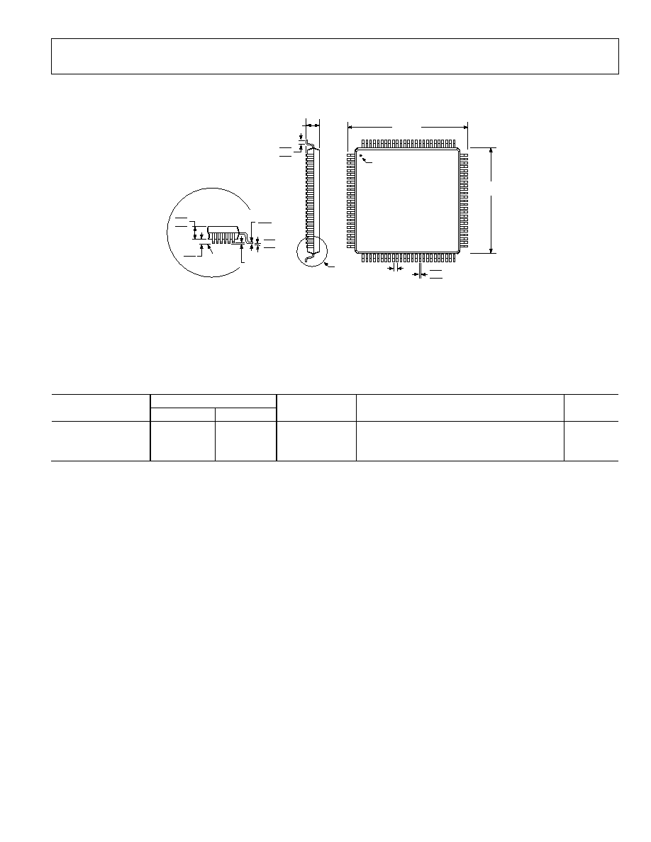
AD9396
Rev. 0 | Page 45 of 48
OUTLINE DIMENSIONS
COMPLIANT TO JEDEC STANDARDS MS-026-BED
TOP VIEW
(PINS DOWN)
1
25
26
51
50
75
76
100
0.50
BSC
LEAD PITCH
0.27
0.22
0.17
1.60 MAX
0.75
0.60
0.45
VIEW A
16.00
BSC SQ
14.00
BSC SQ
PIN 1
1.45
1.40
1.35
0.15
0.05
0.20
0.09
0.08 MAX
COPLANARITY
VIEW A
ROTATED 90° CCW
SEATING
PLANE
7°
3.5°
0°
Figure 18. 100-Lead Low Profile Quad Flat Package [LQFP]
(ST-100)
Dimensions shown in millimeters
ORDERING GUIDE
Max Speeds (MHz)
Temperature
Package
Model Analog
Digital
Range
Package
Description
Option
AD9396KSTZ-100
1
100
100
0°C to 70°C
100-Lead Low Profile Quad Flat Package (LQFP)
ST-100
AD9396KSTZ-150
1
150
150
0°C to 70°C
100-Lead Low Profile Quad Flat Package (LQFP)
ST-100
AD9396/PCB
Evaluation
Board
1
Z = Pb-free part.

AD9396
Rev. 0 | Page 46 of 48
NOTES

AD9396
Rev. 0 | Page 47 of 48
NOTES

AD9396
Rev. 0 | Page 48 of 48
NOTES
Purchase of licensed I
2
C components of Analog Devices or one of its sublicensed Associated Companies conveys a license for the purchaser under the Philips I
2
C Patent
Rights to use these components in an I
2
C system, provided that the system conforms to the I
2
C Standard Specification as defined by Philips.
© 2005 Analog Devices, Inc. All rights reserved. Trademarks and
registered trademarks are the property of their respective owners.
D05690-0-10/05(0)
Document Outline
- þÿ
- þÿ
- þÿ
- FUNCTIONAL BLOCK DIAGRAM
- þÿ
- þÿ
- þÿ
- þÿ
- þÿ
- þÿ
- þÿ
- þÿ
- þÿ
- þÿ
- þÿ
- þÿ
- þÿ
- þÿ
- þÿ
- þÿ
- þÿ
- þÿ
- þÿ
- þÿ
- þÿ
- þÿ
- þÿ
- þÿ
- þÿ
- þÿ
- þÿ
- þÿ
- þÿ
- þÿ
- þÿ
- þÿ
- þÿ
- þÿ