Äîêóìåíòàöèÿ è îïèñàíèÿ www.docs.chipfind.ru
REV. B
Information furnished by Analog Devices is believed to be accurate and
reliable. However, no responsibility is assumed by Analog Devices for its
use, nor for any infringements of patents or other rights of third parties
which may result from its use. No license is granted by implication or
otherwise under any patent or patent rights of Analog Devices.
a
AD9058
One Technology Way, P.O. Box 9106, Norwood, MA 02062-9106, U.S.A.
Tel: 781/329-4700
World Wide Web Site: http://www.analog.com
Fax: 781/326-8703
© Analog Devices, Inc., 2000
Dual 8-Bit 50 MSPS
A/D Converter
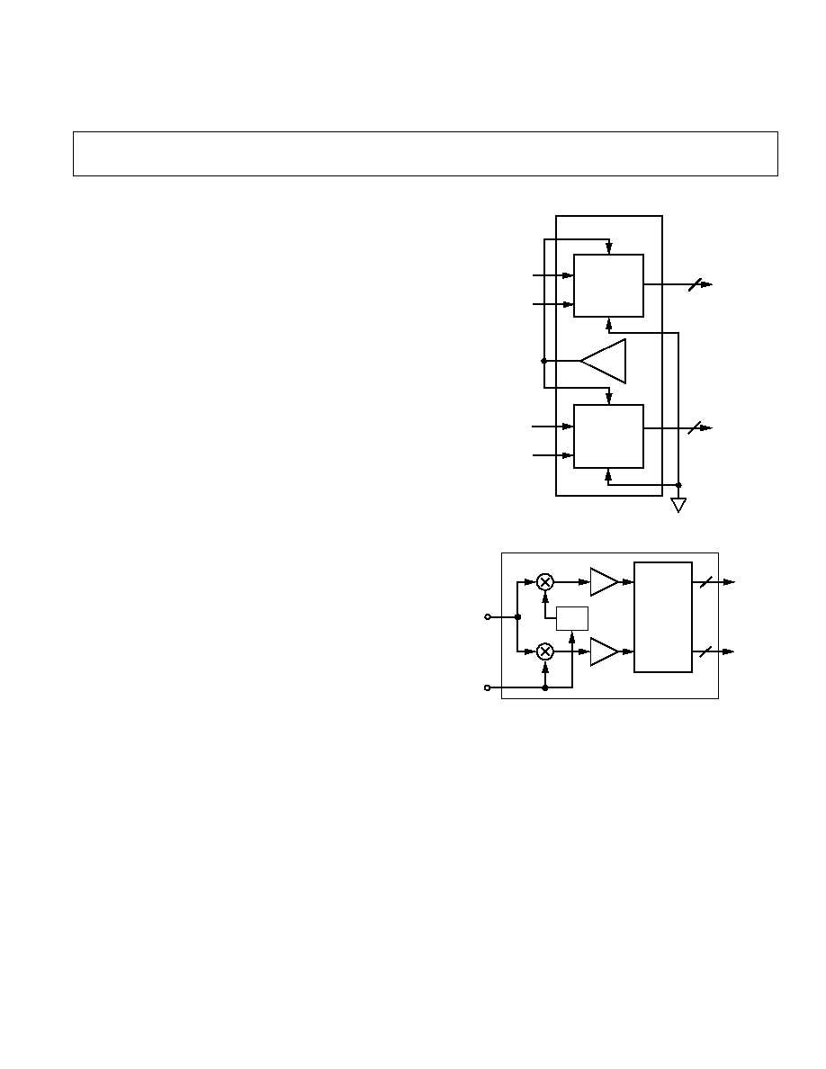
FUNCTIONAL BLOCK DIAGRAM
ENCODE
A
IN
8-BIT
ANALOG-
TO-
DIGITAL
CONVERTER
8
+V
REF
+2 V
REF
ENCODE
AD9058
8-BIT
ANALOG-
TO-
DIGITAL
CONVERTER
8
A
B
V
REF
V
REF
+V
REF
A
IN
QUADRATURE RECEIVER
8
Q
8
I
RF
LO
G
G
AD9058
90°
GENERAL DESCRIPTION
The AD9058 combines two independent high performance
8-bit analog-to-digital converters (ADCs) on a single mono-
lithic IC. Combined with an optional onboard voltage refer-
ence, the AD9058 provides a cost effective alternative for
systems requiring two or more ADCs.
Dynamic performance (SNR, ENOB) is optimized to provide
up to 50 MSPS conversion rates. The unique architecture
results in low input capacitance while maintaining high per-
formance and low power (<0.5 watt/channel). Digital inputs
and outputs are TTL compatible.
Performance has been optimized for an analog input of 2 V
p-p (
± 1 V; 0 V to +2 V). Using the onboard +2 V voltage
reference, the AD9058 can be set up for unipolar positive
operation (0 V to +2 V). This internal voltage reference can
drive both ADCs.
Commercial (0
°C to +70°C) and military (55°C to +125°C)
temperature range parts are available. Parts are supplied in
hermetic 48-lead DIP and 44-lead "J" lead packages.
FEATURES
Two Matched ADCs on Single Chip
50 MSPS Conversion Speed
On-Board Voltage Reference
Low Power (<1W)
Low Input Capacitance (10 pF)
65 V Power Supplies
Flexible Input Range
APPLICATIONS
Quadrature Demodulation for Communications
Digital Oscilloscopes
Electronic Warfare
Radar

REV. B
2
AD9058SPECIFICATIONS
ABSOLUTE MAXIMUM RATINGS
1
Analog Input . . . . . . . . . . . . . . . . . . . . . . . . . 1.5 V to +2.5 V
+V
S
. . . . . . . . . . . . . . . . . . . . . . . . . . . . . . . . . . . . . . . . . +6 V
V
S
. . . . . . . . . . . . . . . . . . . . . . . . . . . . . . . . +0.8 V to 6 V
2
Digital Inputs . . . . . . . . . . . . . . . . . . . . . . . . . . 0.5 V to +V
S
Digital Output Current . . . . . . . . . . . . . . . . . . . . . . . . 20 mA
Voltage Reference Current . . . . . . . . . . . . . . . . . . . . . . .53 mA
+V
REF
. . . . . . . . . . . . . . . . . . . . . . . . . . . . . . . . . . . . . +2.5 V
V
REF
. . . . . . . . . . . . . . . . . . . . . . . . . . . . . . . . . . . . . . . 1.5
Operating Temperature Range
AD9058JD/JJ/KD/KJ . . . . . . . . . . . . . . . . . . . 0
°C to +70°C
Maximum Junction Temperature
3
AD9058JD/JJ/KD/KJ . . . . . . . . . . . . . . . . . . . . . . . . +175
°C
Storage Temperature Range . . . . . . . . . . . . 65
°C to +150°C
Lead Temperature (Soldering, 10 sec) . . . . . . . . . . . . +300
°C
ELECTRICAL CHARACTERISTICS
[ V
S
= 5 V; V
REF
= +2 V (internal); ENCODE = 40 MSPS; A
IN
= 0 V to +2 V; V
REF
=
GROUND, unless otherwise noted.]
2
All specifications apply to either of the two ADCs
Test
AD9058JD/JJ
AD9058KD/KJ
Parameter (Conditions)
Temp
Level
Min
Typ
Max
Min
Typ
Max
Unit
RESOLUTION
8
8
Bits
DC ACCURACY
Differential Nonlinearity
+25
°C
I
0.25
0.65
0.25
0.5
LSB
Full
VI
0.8
0.7
LSB
Integral Nonlinearity
+25
°C
I
0.5
1.3
0.5
1.0
LSB
Full
VI
1.4
1.25
LSB
No Missing Codes
Full
VI
GUARANTEED
GUARANTEED
ANALOG INPUT
Input Bias Current
+25
°C
I
75
170
75
170
µA
Full
VI
340
340
µA
Input Resistance
+25
°C
I
12
28
12
28
k
Input Capacitance
+25
°C
IV
10
15
10
15
pF
Analog Bandwidth
+25
°C
V
175
175
MHz
REFERENCE INPUT
Reference Ladder Resistance
+25
°C
I
120
170
220
120
170
220
Full
VI
80
270
80
270
Ladder Tempco
Full
V
0.45
0.45
/°C
Reference Ladder Offset
+25
°C
I
8
16
8
16
mV
(Top)
Full
VI
24
24
mV
Reference Ladder Offset
+25
°C
I
8
23
8
23
mV
(Bottom)
Full
VI
33
33
mV
Offset Drift Coefficient
Full
V
50
50
µV/°C
INTERNAL VOLTAGE REFERENCE
Reference Voltage
+25
°C
I
1.95
2.0
2.20
1.95
2.0
2.20
V
Full
VI
1.90
2.25
1.90
2.25
V
Temperature Coefficient
Full
V
150
150
µV/°C
Power Supply Rejection
Ratio (PSRR)
+25
°C
I
10
25
10
25
mV/V
SWITCHING PERFORMANCE
Maximum Conversion Rate
4
+25
°C
I
50
50
60
MSPS
Aperture Delay (t
A
)
+25
°C
IV
0.1
0.8
1.5
0.1
0.8
1.5
ns
Aperture Delay Matching
+25
°C
IV
0.2
0 5
0.2
0.5
ns
Aperture Uncertainty (Jitter)
+25
°C
V
10
10
ps, rms
Output Delay (Valid) (t
V
)
4
+25
°C
I
8
5
8
ns
Output Delay (t
V
) Tempco
Full
V
16
16
ps/
°C
Propagation Delay (t
PD
)
4
+25
°C
I
12
12
19
ns
Propagation Delay (t
PD
) Tempco
Full
V
16
16
ps/
°C
Output Time Skew
+25
°C
V
1
1
ns
ENCODE INPUT
Logic "1" Voltage
Full
VI
2
2
V
Logic "0" Voltage
Full
VI
0.8
0.8
V
Logic "1" Current
Full
VI
600
600
µA
Logic "0" Current
Full
VI
1000
1000
µA
Input Capacitance
+25
°C
V
5
5
pF
Pulsewidth (High)
+25
°C
I
8
8
ns
Pulsewidth (Low)
+25
°C
I
8
8
ns
REV. B
3
AD9058
Test
AD9058JD/JJ
AD9058KD/KJ
Parameter (Conditions)
Temp
Level
Min
Typ
Max
Min
Typ
Max
Unit
DYNAMIC PERFORMANCE
Transient Response
+25
°C
V
2
2
ns
Overvoltage Recovery Time
+25
°C
V
2
2
ns
Effective Number of Bits (ENOB)
5
Analog Input @ 2.3 MHz
+25
°C
I
7.7
7.2
7.7
Bits
@ 10.3 MHz
+25
°C
I
7.4
7.1
7.4
Bits
Signal-to-Noise Ratio
5
Analog Input @ 2.3 MHz
+25
°C
I
48
45
48
dB
@ 10.3 MHz
+25
°C
I
46
44
46
dB
Signal-to-Noise Ratio
5
(Without Harmonics)
Analog Input @ 2.3 MHz
+25
°C
I
48
46
48
dB
@ 10.3 MHz
+25
°C
I
47
45
47
dB
2nd Harmonic Distortion
Analog Input @ 2.3 MHz
+25
°C
I
58
48
58
dBc
@ 10.3 MHz
+25
°C
I
58
48
58
dBc
3rd Harmonic Distortion
Analog Input @ 2.3 MHz
+25
°C
I
58
50
58
dBc
@ 10.3 MHz
+25
°C
I
58
50
58
dBc
Crosstalk Rejection
6
+25
°C
IV
60
48
60
dBc
DIGITAL OUTPUTS
Logic "1" Voltage (I
OH
= 2 mA)
Full
VI
2.4
2.4
V
Logic "0" Voltage (I
OL
= 2 mA)
Full
VI
0.4
0.4
V
POWER SUPPLY
7
+V
S
Supply Current
Full
VI
127
154
127
154
mA
V
S
Supply Current
Full
VI
27
38
27
38
mA
Power Dissipation
Full
VI
770
960
770
960
mW
NOTES
1
Absolute maximum ratings are limiting values to be applied individually, and beyond which the serviceability of the circuit may be impaired. Functional operability is
not necessarily implied. Exposure to absolute maximum rating conditions for an extended period of time may affect device reliability.
2
For applications in which +V
S
may be applied before V
S
, or +V
S
current is not limited to 500 mA, a reverse biased clamping diode should be inserted between
ground and V
S
to prevent destructive latch up. See section entitled "Using the AD9058."
3
Typical thermal impedances: 44-lead hermetic J-Leaded ceramic package:
JA
= 86.4
°C/W;
JC
= 24.9
°C/W; 48-lead hermetic DIP
JA
= 40
°C/W;
JC
= 12
°C/W.
4
To achieve guaranteed conversion rate, connect each data output to ground through a 2 k
pull-down resistor.
5
SNR performance limits for the 48-lead DIP "D" package are 1 dB less than shown. ENOB limits are degraded by 0.3 dB. SNR and ENOB measured with
analog input signal 1 dB below full scale at specified frequency.
6
Crosstalk rejection measured with full-scale signals of different frequencies (2.3 MHz and 3.5 MHz) applied to each channel. With both signals synchronously
encoded at 40 MSPS, isolation of the undesired frequency is measured with an FFT.
7
Applies to both A/Ss and includes internal ladder dissipation.
Specifications subject to change without notice.
EXPLANATION OF TEST LEVELS
Test Level
I
100% production tested.
II
100% production tested at +25
°C, and sample tested at
specified temperatures.
III Sample tested only.
IV Parameter is guaranteed by design and characterization
testing.
V
Parameter is a typical value only.
VI All devices are 100% production tested at +25
°C. 100%
production tested at temperature extremes for extended
temperature devices; sample tested at temperature
extremes for commercial/industrial devices.
ORDERING GUIDE
Temperature
Package
Model
Range
Description
Option
1
AD9058JJ
0
°C to +70°C
44-Lead J-Leaded
J-44
Ceramic
2
AD9058KJ
0
°C to +70°C
44-Lead J-Leaded
J-44
Ceramic, AC Tested
AD9058TJ/883
3
55
°C to +125°C 44-Lead J-Leaded
J-44
Ceramic, AC Tested
AD9058JD
0
°C to +70°C
48-Lead Ceramic DIP D-48
AD9058KD
0
°C to +70°C
48-Lead Ceramic
D-48
DIP, AC Tested
AD9058TD/883
3
55
°C to +125°C 48-Lead Ceramic
D-48
DIP, AC Tested
NOTES
1
D = Hermetic Ceramic DIP Package; J = Leaded Ceramic Package.
2
Hermetically sealed ceramic package; footprint equivalent to PLCC.
3
For specifications, refer to Analog Devices Military Products Databook.
REV. B
AD9058
4
CAUTION
ESD (electrostatic discharge) sensitive device. Electrostatic charges as high as 4000 V readily
accumulate on the human body and test equipment and can discharge without detection. Although
the AD9058 features proprietary ESD protection circuitry, permanent damage may occur on
devices subjected to high energy electrostatic discharges. Therefore, proper ESD precautions are
recommended to avoid performance degradation or loss of functionality.
WARNING!
ESD SENSITIVE DEVICE
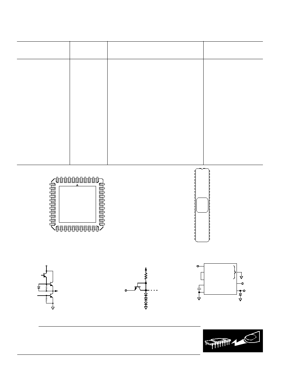
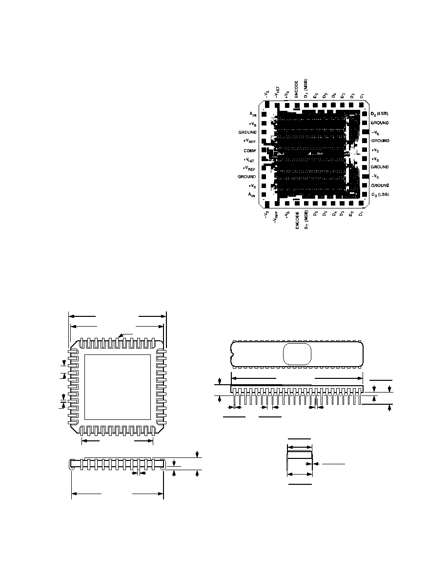
PIN DESCRIPTIONS
J-Lead
Ceramic DIP
Pin Number
Pin Number
ADC-A
ADC-B
Name
Function
ADC-A
ADC-B
3
43
+V
REF
Top of internal voltage reference ladder.
14
11
4
42
GROUND
Analog ground return.
15
10
5
41
+V
S
Positive 5 V analog supply voltage.
16
9
6
40
AIN
Analog input voltage.
17
8
7
39
V
S
Negative 5 V supply voltage.
19
6
8
38
V
REF
Bottom of internal voltage reference ladder.
20
5
9
37
+V
S
Positive 5 V digital supply voltage.
22
3
10
36
ENCODE
TTL compatible convert command.
23
2
11
35
D7 (MSB)
Most significant bit of TTL digital output.
25
48
1217
3429
D6D1
TTL compatible digital output bits.
2631
4742
18
28
D0 (LSB)
Least significant bit of TTL digital output.
32
41
19
27
GROUND
Digital ground return.
21, 24, 33
1, 4, 40
20
26
V
S
Negative 5 V supply voltage.
34
39
21
25
GROUND
Analog ground return.
35
38
22
24
+V
S
Positive 5 V analog supply voltage.
36
37
COMMON PINS
COMMON PINS
1
COMP
Connection for external (0.1
µF)
12
compensation capacitor.
2
+V
INT
Internal +2 V reference; can drive
13
+V
REF
for both ADCs.
7
17
18
28
39
29
GROUND
GROUND
6
A
IN
+V
REF
COMP
NC
ENCODE
GROUND
GROUND
GROUND
V
S
NC
GROUND
D
0
(LSB)
V
S
V
REF
+V
S
ENCODE
D
7
(MSB)
D
6
40
TOP VIEW
(Not to Scale)
AD9058
NC = NO CONNECT
GROUND
D
5
D
4
D
3
D
2
D
1
V
S
V
REF
+V
S
D
7
(MSB)
D
6
D
5
D
4
D
3
D
2
D
1
+V
S
+V
S
V
S
D
0
(LSB)
+V
S
+V
INT
+V
REF
+V
S
A
IN
AD9058JJ/KJ Pinouts
24
25
48
1
D
7
(MSB)
GROUND
GROUND
GROUND
GROUND
D
0
(LSB)
D
6
GROUND
COMP
GROUND
A
IN
V
REF
+V
S
ENCODE
ENCODE
NC
NC
NC = NO CONNECT
GROUND
GROUND
GROUND
GROUND
V
S
+V
S
+V
REF
+V
INT
+V
REF
+V
S
A
IN
V
S
V
REF
+V
S
V
S
+V
S
+V
S
V
S
D
5
D
4
D
3
D
2
D
1
D
7
(MSB)
D
0
(LSB)
D
6
D
5
D
4
D
3
D
2
D
1
AD9058JD/KD Pinouts
DIGITAL BITS
+V
S
AD9058 Equivalent Digital Outputs
+5.0V
13k
ENCODE
AD9058 Equivalent Encode Circuit
AD9058 Burn-In Connections
AD9058
ENCODE**
**
INDICATES EACH PIN IS CONNECTED THROUGH 100
* INDICATES EACH PIN IS CONNECTED THROUGH 2 k
A
IN
**
V
REF
+V
S
V
S
5.2V
+5V
GROUND
COMP
+V
REF
+V
INT
D
0
D
7
*
+V
S
0.1 F
REV. B
AD9058
5
THEORY OF OPERATION
The AD9058 contains two separate 8-bit analog-to-digital con-
verters (ADCs) on a single silicon die. The two devices can be
operated independently with separate analog inputs, voltage
references and clocks.
In a traditional flash converter, 256 input comparators are required
to make the parallel conversion for 8-bit resolution. This is in
marked contrast to the scheme used in the AD9058, as shown
in Figure 1.
Unlike traditional "flash," or parallel, converters, each of the two
ADCs in the AD9058 utilizes a patented interpolating archi-
tecture to reduce circuit complexity, die size and input capacitance.
These advantages accrue because, compared to a conventional
flash design, only half the normal number of input comparator
cells is required to accomplish the conversion.
In this unit, each of the two independent ADCs uses only 128
(2
7
) comparators to make the conversion. The conversion for
the seven most significant bits (MSBs) is performed by the 128
comparators. The value of the least significant bit (LSB) is
determined by interpolation between adjacent comparators in
the decoding register. A proprietary decoding scheme processes
the comparator outputs and provides an 8-bit code to the output
register of each ADC; the scheme also minimizes error codes.
Analog input range is established by the voltages applied at the
voltage reference inputs (+V
REF
and V
REF
). The AD9058 can
operate from 0 V to +2 V using the internal voltage reference,
or anywhere between 1 V and +2 V using external references.
Input range is limited to 2 V p-p when using external references.
The internal resistor ladder divides the applied voltage reference
into 128 steps, with each step representing two 8-bit quantiza-
tion levels.
2
1
INTERPOLATING LATCHES
DECODE LOGIC
LATCHES
256
8
8
128
127
ANALOG IN
V
REF
+V
REF
Figure 1. AD9058 Comparator Block Diagram
The onboard voltage reference, +V
INT
, is a bandgap reference
which has sufficient drive capability for both reference ladders.
It provides a +2 V reference that can drive both ADCs in the
AD9058 for unipolar positive operation (0 V to +2 V).
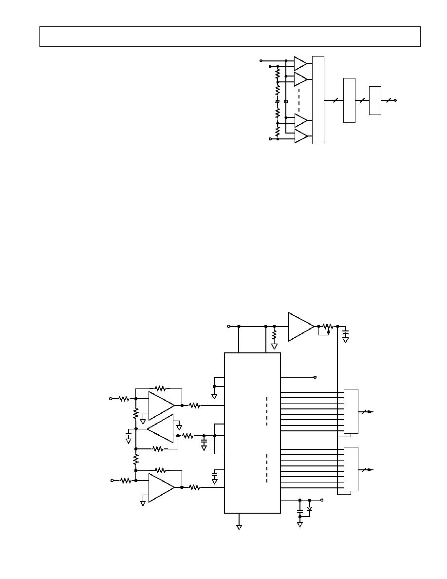
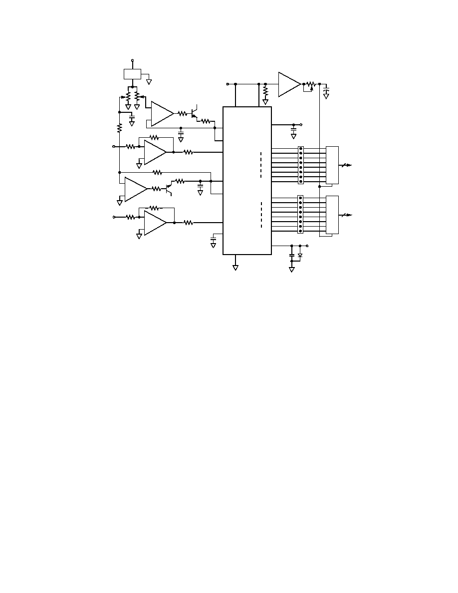
USING THE AD9058
Refer to Figure 2. Using the internal voltage reference con-
nected to both ADCs as shown reduces the number of external
components required to create a complete data acquisition sys-
tem. The input ranges of the ADCs are positive unipolar in this
configuration, ranging from 0 V to +2 V. Bipolar input signals
are buffered, amplified and offset into the proper input range of
the ADC using a good low distortion amplifier such as the
AD9617 or AD9618.
18
28
ENCODE
A
ENCODE
B
3
43
8
38
10pF
1k
74HCT04
50
5, 9, 22,
24, 37, 41
+5V
D
0B
(LSB)
D
7B
(MSB)
8
8
74HCT 273
CLOCK
CLOCK
V
S
7, 20,
26, 39
0.1µF
1N4001
4,19, 21
25, 27, 42
ENCODE
10
36
AD9058
74HCT 273
ANALOG
IN B
±0.5 V
AD9617
400
200
5
ANALOG
IN A
±0.5 V
0.1µF
AD9617
400
200
5
20k
20k
800
AD707
800
6
2
+V
INT
COMP
1
0.1µF
0.1µF
+2V
40
(J-LEAD)
2V
+
+
+
5V
17
16
15
14
13
12
11
29
30
31
32
33
34
35
(SEE TEXT)
+V
S
D
0A
(LSB)
D
7A
(MSB)
+V
REF A
+V
REF B
A
IN A
V
REF A
V
REF B
A
IN B
Figure 2. AD9058 Using Internal +2 V Voltage Reference
REV. B
AD9058
6
18
RZ1
28
ANALOG
IN B
±0.125 V
AD9618
400
50
5k
ANALOG
IN A
±0.125 V
AD580
1
3
2
10k
10k
0.1µF
1/2
AD708
+5V
+5V
20k
+V
REF A
ENCODE
A
ENCODE
B
AD9618
400
50
1/2
AD708
5
20k
3
43
8
38
10
150
150
10
10pF
1k
50k
5, 9, 22,
24, 37, 41
+5V
RZ2
D
0A
(LSB)
D
7A
(MSB)
D
0B
(LSB)
D
7B
(MSB)
8
74ACT 273
8
74ACT 273
CLOCK
CLOCK
V
S
7, 20,
26, 39
0.1µF
1N4001
4,19, 21
25, 27, 42
RZ1, RZ2 = 2,000
SIP (8/PKG)
ENCODE
10
36
2N3904
0.1µF
0.1µF
+1V
±1V
1V
2N3906
±1 V
0.1µF
COMP
1
0.1µF
6
40
AD9058
(J-LEAD)
74ACT04
5V
+
+
+
+
17
16
15
14
13
12
11
29
30
31
32
33
34
35
5V
(SEE TEXT)
+V
REF B
A
IN A
V
REF A
V
REF B
A
IN B
+V
S
Figure 3. AD9058 Using External Voltage References
The AD9058 offers considerable flexibility in selecting the ana-
log input ranges of the ADCs; the two independent ADCs can
even have different input ranges if required. In Figure 3 above,
the AD9058 is shown configured for
±1 V operation.
The Reference Ladder Offset shown in the specifications table re-
fers to the error between the voltage applied to the +V
REF
(top)
or V
REF
(bottom) of the reference ladder and the voltage re-
quired at the analog input to achieve a 1111 1111 or 0000 0000
transition. This indicates the amount of adjustment range which
must be designed into the reference circuit for the AD9058.
The diode shown between ground and V
S
is normally reverse
biased and is used to prevent latch-up. Its use is recommended
for applications in which power supply sequencing might allow
+V
S
to be applied before V
S
; or the +V
S
supply is not current
limited. If the negative supply is allowed to float (the +5 V sup-
ply is powered up before the 5 V supply), substantial +5 V
supply current will attempt to flow through the substrate (V
S
supply contact) to ground. If this current is not limited to <500
mA, the part may be destroyed. The diode prevents this poten-
tially destructive condition from occurring.
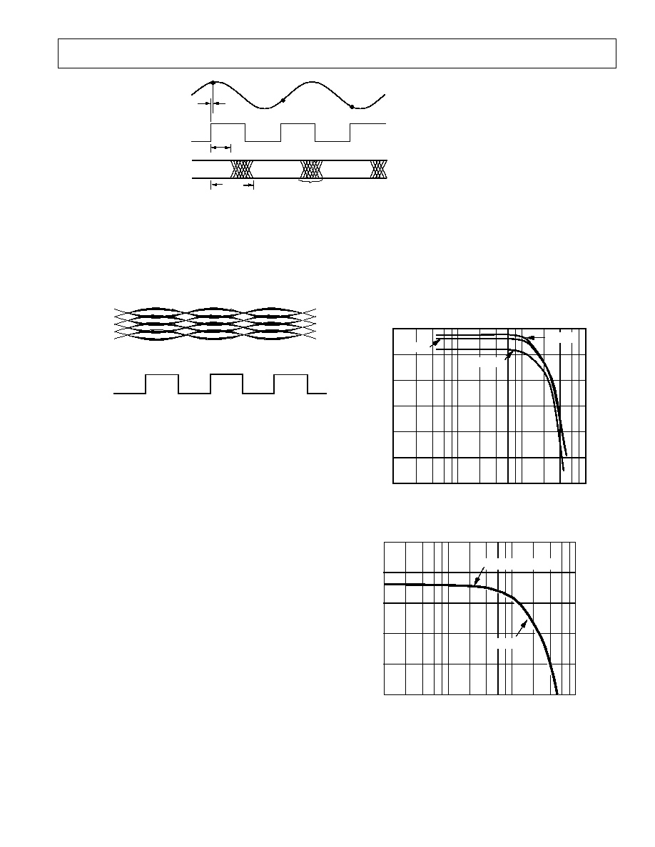
Timing
Refer to the AD9058 Timing Diagram. The AD9058 provides
latched data outputs with no pipeline delay. To conserve power,
the data outputs have relatively slow rise and fall times. When
designing system timing, it is important to observe (1) set-up
and hold times; and (2) the intervals when data is changing.
Figure 3 shows 2 k
pull-down resistors on each of the D
0
D
7
output data bits. When operating at conversion rates higher than
40 MSPS, these resistors help equalize rise and fall times and
ease latching the output data into external latches. The 74ACT
logic family devices have short set-up and hold times and are the
recommended choices for speeds of 40 MSPS or more.
Layout
To insure optimum performance, a single low-impedance ground
plane is recommended. Analog and digital grounds should be
connected together and to the ground plane at the AD9058 de-
vice. Analog and digital power supplies should be bypassed to
ground through 0.1
µF ceramic capacitors as close to the unit as
possible.
An evaluation board (ADI part #AD9058/PCB) is available to
aid designers and provide a suggested layout. The use of sockets
may limit the dynamic performance of the part and is not rec-
ommended except for prototype or evaluation purposes.
For prototyping or evaluation, surface mount sockets are available
from Methode (part #213-0320602) for evaluating AD9058 sur-
face mount packages. To evaluate the AD9058 in through-hole
PCB designs, use the AD9058JD/KD with individual pin sockets
(AMP part #6-330808-0). Alternatively, surface mount AD9058
units can be mounted in a through-hole socket (Circuit Assembly
Corporation, Irvine California part #CA-44SPC-T).
AD9058 APPLICATIONS
Combining two ADCs in a single package is an attractive alter-
native in a variety of systems when cost, reliability and space are
important considerations. Different systems emphasize particu-
lar specifications, depending on how the part is used.
In high density digital radio communications, a pair of high
speed ADCs are used to digitize the in-phase (I) and quadrature
(Q) components of a modulated signal. The signal presented to
each ADC in this type of system consists of message-dependent
amplitudes varying at the symbol rate, which is equal to the
sample rates of the converters.
REV. B
AD9058
7
t
V
t
PD
N
t
A
N + 1
ANALOG INPUT
ENCODE
D D
0
7
DATA
CHANGING
VALID DATA
FOR N 1
VALID DATA
FOR N
VALID DATA
FOR N + 1
N + 2
t
V
= DATA DELAY OF
PRECEDING ENCODE
t
PD
= OUTPUT PROPAGATION DELAY
= APERTURE TIME
t
A
Figure 4. AD9058 Timing Diagram
Figure 5 below shows what the analog input to the AD9058 would
look like when observed relative to the sample clock. Signal-
to-noise ratio (SNR), transient response, and sample rate are all
critical specifications in digitizing this "eye pattern."
ANALOG
INPUT
SAMPLE
CLOCK
Figure 5. AD9058 I and Q Input Signals
Receiver sensitivity is limited by the SNR of the system. For the
ADC, SNR is measured in the frequency domain and calculated
with a Fast Fourier Transform (FFT). The signal-to-noise ratio
equals the ratio of the fundamental component of the signal
(rms amplitude) to the rms level of the noise. Noise is the sum
of all other spectral components, including harmonic distortion,
but excluding dc.
Although the signal being sampled does not have a significant
slew rate at the instant it is encoded, dynamic performance of
the ADC and the system is still critical. Transient response is the
time required for the AD9058 to achieve full accuracy when a
step function input is applied. Overvoltage recovery time is the in-
terval required for the AD9058 to recover to full accuracy after
an overdriven analog input signal is reduced to its input range.
Time domain performance of the ADC is also extremely impor-
tant in digital oscilloscopes. When a track (sample)-and-hold is
used ahead of the ADC, its operation becomes similar to that
described above for receivers.
The dynamic response to high-frequency inputs can be described
by the effective number of bits (ENOB). The effective number of bits
is calculated with a sine wave curve fit and is expressed as:
ENOB = N LOG
2
[Error (measured)/Error (ideal)]
where N is the resolution (number of bits) and measured error
is actual rms error calculated from the converter's outputs with
a pure sine wave applied as the input.
Maximum conversion rate is defined as the encode (sample) rate
at which SNR of the lowest frequency analog test signal drops
no more than 3 dB below the guaranteed limit.
HARMONIC DISTORTION
dB
60
55
50
45
40
35
INPUT FREQUENCY MHz
0.1
1
10
100
30
+25°C
55°C
+125°C
Figure 6. Harmonic Distortion vs. Analog Input Frequency
0.1
1
10
100
INPUT FREQUENCY MHz
8.0
7.2
6.4
5.5
EFFECTIVE NO. OF BITS (ENOB)
55
50
45
40
35
30
SIGNAL-TO-NOISE RATIO (SNR)
dB
+25°C AND +125°C
55°C
Figure 7. AD9058 Dynamic Performance vs. Analog Input
Frequency
REV. B
8
C147405/00 (rev. B) 00562
PRINTED IN U.S.A.
AD9058
OUTLINE DIMENSIONS
Dimensions shown in inches and (mm).
Die Dimensions . . . . . . . . . . . . . . . . 106
× 108 × 15 (±2) mils
Pad Dimensions . . . . . . . . . . . . . . . . . . . . . . . . . . . . 4
× 4 mils
Metalization . . . . . . . . . . . . . . . . . . . . . . . . . . . . . . . . . . . Gold
Backing . . . . . . . . . . . . . . . . . . . . . . . . . . . . . . . . . . . . . None
Substrate Potential . . . . . . . . . . . . . . . . . . . . . . . . . . . . . . V
S
Passivation . . . . . . . . . . . . . . . . . . . . . . . . . . . . . . . . . . Nitride
Die Attach . . . . . . . . . . . . . . . . . . . . Gold Eutectic (Ceramic)
Bond Wire . . . . . . . . . . . . 11.3 mil, Gold; Gold Ball Bonding
MECHANICAL INFORMATION
44-Lead J-Leaded Ceramic (J-44) Package
48-Lead Hermetic Ceramic DIP (D-48) Package
0.050 TYP
(1.27)
0.020 TYP
(0.508)
PIN 1
0.690 ± 0.012 SQ.
(17.5 ± 0.305)
0.650 ±0.008 SQ.
(16.51 ±0.203)
0.500 ±0.008
(12.70 ± 0.203)
7
17
18
28
39
29
40
6
0.135 (3.42)
MAX
0.017 (0.432)
TYP
0.630 ± 0.020
(16.0 ± 0.058)
0.037 ± 0.012
(0.940 ± 0.305)
0.62 (15.75)
0.59 (12.95)
0.015 (0.38)
0.008 (0.20)
0.63 (16.00)
0.52 (13.21)
0.70 MAX
(1.77 MAX)
2.400 ± 0.024
(60.96 ± 0.609)
0.225 MAX
(5.72 MAX)
1
24
25
48
0.150
(3.81)
MIN
0.023 (0.58)
0.014 (0.36)
0.110 (2,79)
0.090 (2.29)
0.060 (1.52)
0.015 (0.38)