Äîêóìåíòàöèÿ è îïèñàíèÿ www.docs.chipfind.ru
REV. A
Information furnished by Analog Devices is believed to be accurate and
reliable. However, no responsibility is assumed by Analog Devices for its
use, nor for any infringements of patents or other rights of third parties
which may result from its use. No license is granted by implication or
otherwise under any patent or patent rights of Analog Devices.
a
AD8138
One Technology Way, P.O. Box 9106, Norwood, MA 02062-9106, U.S.A.
Tel: 781/329-4700
World Wide Web Site: http://www.analog.com
Fax: 781/326-8703
© Analog Devices, Inc., 1999
Low Distortion
Differential ADC Driver
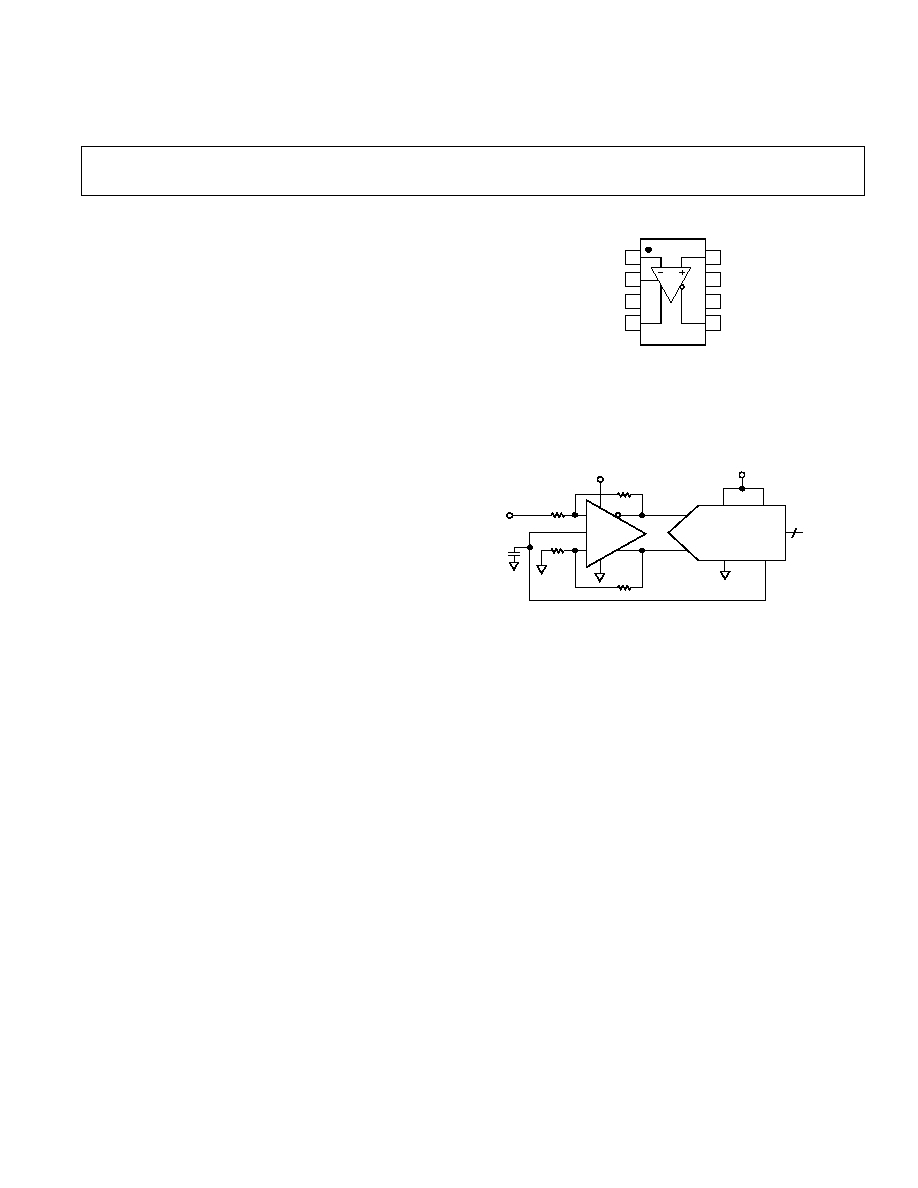
FUNCTIONAL BLOCK DIAGRAM
1
2
3
4
8
7
6
5
AD8138
NC
V
OCM
OUT
V+
NC = NO CONNECT
+IN
V
IN
+OUT
FEATURES
Easy to Use Single-Ended-to-Differential Conversion
Adjustable Output Common-Mode Voltage
Externally Adjustable Gain
Low Harmonic Distortion
94 dBc--Second, <114 dBc--Third @ 5 MHz into
800 Load
87 dBc--Second, 85 dBc--Third @ 20 MHz into
800 Load
3 dB Bandwidth of 320 MHz, G = +1
Fast Settling to 0.01% of 16 ns
Slew Rate 1150 V/ s
Fast Overdrive Recovery of 4 ns
Low Input Voltage Noise of 5 nV/
Hz
1 mV Typical Offset Voltage
Wide Supply Range +3 V to 5 V
Low Power 90 mW on +5 V
0.1 dB Gain Flatness to 40 MHz
Available in 8-Lead SOIC
APPLICATIONS
ADC Driver
Single-Ended-to-Differential Converter
IF and Baseband Gain Block
Differential Buffer
Line Driver
PRODUCT DESCRIPTION
AD8138 is a major advancement over op amps for differential
signal processing. The AD8138 can be used as a single-ended-
to-differential amplifier or as a differential-to-differential ampli-
fier. The AD8138 is as easy to use as an op amp, and greatly
simplifies differential signal amplification and driving.
Manufactured on ADI's proprietary XFCB bipolar process, the
AD8138 has a 3 dB bandwidth of 320 MHz and delivers a
differential signal with the lowest harmonic distortion available
in a differential amplifier. The AD8138 has a unique internal
feedback feature that provides output gain and phase matching
that are balanced, suppressing even order harmonics. The inter-
nal feedback circuit also minimizes any gain error that would be
associated with the mismatches in the external gain setting
resistors.
The AD8138's differential output helps balance the input-to-
differential ADCs, maximizing the performance of the ADC.
The AD8138 eliminates the need for a transformer with high
performance ADCs, preserving the low frequency and dc infor-
mation. The common-mode level of the differential output is
adjustable by a voltage on the V
OCM
pin, easily level-shifting
the input signals for driving single supply ADCs. Fast overload
recovery preserves sampling accuracy.
The AD8138 distortion performance makes it an ideal ADC
driver for communication systems, with distortion performance
good enough to drive state-of-the-art 10- to 16-bit converters
at high frequencies. The AD8138's high bandwidth and IP3
also make it appropriate for use as a gain block in IF and
baseband signal chains. The AD8138 offset and dynamic per-
formance make it well suited for a wide variety of signal pro-
cessing and data acquisition applications.
The AD8138 is offered in an 8-lead SOIC that operates over
the industrial temperature range of 40
°
C to +85
°
C.
TYPICAL APPLICATION CIRCUIT
AIN
AIN
AVDD
DVDD
AVSS
V
REF
ADC
499
499
499
499
V
IN
V
OCM
+5V
+5V
DIGITAL
OUTPUTS
AD8138
+

2
REV. A
AD8138SPECIFICATIONS
AD8138
Parameter
Conditions
Min
Typ
Max
Units
D
IN
to OUT Specifications
DYNAMIC PERFORMANCE
3 dB Small Signal Bandwidth
V
OUT
= 0.5 V p-p, C
F
= 0 pF
290
320
MHz
V
OUT
= 0.5 V p-p, C
F
= 1 pF
225
MHz
Bandwidth for 0.1 dB Flatness
V
OUT
= 0.5 V p-p, C
F
= 0 pF
30
MHz
Large Signal Bandwidth
V
OUT
= 2 V p-p, C
F
= 0 pF
265
MHz
Slew Rate
V
OUT
= 2 V p-p, C
F
= 0 pF
1150
V/
µ
s
Settling Time
0.01%, V
OUT
= 2 V p-p, C
F
= 1 pF
16
ns
Overdrive Recovery Time
V
IN
= 5 V to 0 V Step, G = +2
4
ns
NOISE/HARMONIC PERFORMANCE
Second Harmonic
V
OUT
= 2 V p-p, 5 MHz, R
L,dm
= 800
94
dBc
V
OUT
= 2 V p-p, 20 MHz, R
L,dm
= 800
87
dBc
V
OUT
= 2 V p-p, 70 MHz, R
L,dm
= 800
62
dBc
Third Harmonic
V
OUT
= 2 V p-p, 5 MHz, R
L,dm
= 800
114
dBc
V
OUT
= 2 V p-p, 20 MHz, R
L,dm
= 800
85
dBc
V
OUT
= 2 V p-p, 70 MHz, R
L,dm
= 800
57
dBc
IMD
20 MHz
77
dBc
IP3
20 MHz
37
dBm
Voltage Noise (RTI)
f = 100 kHz to 40 MHz
5
nV/
Hz
Input Current Noise
f = 100 kHz to 40 MHz
2
pA/
Hz
INPUT CHARACTERISTICS
Offset Voltage
V
OS,dm
= V
OUT,dm
/2; V
DIN+
= V
DIN
= V
OCM
= 0 V
2.5
±
1
2.5
mV
T
MIN
T
MAX
Variation
±
4
µ
V/
°
C
Input Bias Current
3.5
7
µ
A
T
MIN
T
MAX
Variation
0.01
µ
A/
°
C
Input Resistance
Differential
6
M
Common Mode
3
M
Input Capacitance
1
pF
Input Common-Mode Voltage
4.7 +3.4
V
CMRR
V
OUT,dm
/
V
IN,cm
;
V
IN,cm
=
±
1 V
75
70
dB
OUTPUT CHARACTERISTICS
Output Voltage Swing
Maximum
V
OUT
; Single-Ended Output
7.75
V p-p
Output Current
95
mA
Output Balance Error
V
OUT,cm
/
V
OUT,dm
;
V
OUT,dm
= 1 V
66
dB
V
OCM
to OUT Specifications
DYNAMIC PERFORMANCE
3 dB Bandwidth
250
MHz
Slew Rate
330
V/
µ
s
DC PERFORMANCE
Input Voltage Range
±
3.8
V
Input Resistance
200
k
Input Offset Voltage
V
OS,cm
= V
OUT,cm
; V
DIN+
= V
DIN
= V
OCM
= 0 V
3.5
±
1
3.5
mV
Input Bias Current
0.5
µ
A
V
OCM
CMRR
[
V
OUT,dm
/
V
OCM
];
V
OCM
=
±
1 V
75
dB
Gain
V
OUT,cm
/
V
OCM
;
V
OCM
=
±
1 V
0.9955 1
1.0045
V/V
POWER SUPPLY
Operating Range
±
1.4
±
5.5
V
Quiescent Current
18
20
23
mA
T
MIN
to T
MAX
Variation
40
µ
A/
°
C
Power Supply Rejection Ratio
V
OUT,dm
/
V
S
;
V
S
=
±
1 V
90
70
dB
OPERATING TEMPERATURE RANGE
40
+85
°
C
NOTES
Harmonic Distortion Performance is equal or slightly worse with higher values of R
L,dm
. See Figures 14 and 15 for more information.
Specifications subject to change without notice.
(@ +25 C, V
S
= 5 V, V
OCM
= 0, G = +1, R
L,dm
= 500 , unless otherwise noted.
Refer to Figure 1 for test setup and label descriptions. All specifications refer to single-ended input and differential outputs unless noted.)

3
REV. A
AD8138
SPECIFICATIONS
AD8138
Parameter
Conditions
Min
Typ
Max
Units
D
IN
to OUT Specifications
DYNAMIC PERFORMANCE
3 dB Small Signal Bandwidth
V
OUT
= 0.5 V p-p, C
F
= 0 pF
280
310
MHz
V
OUT
= 0.5 V p-p, C
F
= 1 pF
225
MHz
Bandwidth for 0.1 dB Flatness
V
OUT
= 0.5 V p-p, C
F
= 0 pF
29
MHz
Large Signal Bandwidth
V
OUT
= 2 V p-p, C
F
= 0 pF
265
MHz
Slew Rate
V
OUT
= 2 V p-p, C
F
= 0 pF
950
V/
µ
s
Settling Time
0.01%, V
OUT
= 2 V p-p, C
F
= 1 pF
16
ns
Overdrive Recovery Time
V
IN
= 2.5 V to 0 V Step, G = +2
4
ns
NOISE/HARMONIC PERFORMANCE
Second Harmonic
V
OUT
= 2 V p-p, 5 MHz, R
L,dm
= 800
90
dBc
V
OUT
= 2 V p-p, 20 MHz, R
L,dm
= 800
79
dBc
V
OUT
= 2 V p-p, 70 MHz, R
L,dm
= 800
60
dBc
Third Harmonic
V
OUT
= 2 V p-p, 5 MHz, R
L,dm
= 800
100
dBc
V
OUT
= 2 V p-p, 20 MHz, R
L,dm
= 800
82
dBc
V
OUT
= 2 V p-p, 70 MHz, R
L,dm
= 800
53
dBc
IMD
20 MHz
74
dBc
IP3
20 MHz
35
dBm
Voltage Noise (RTI)
f = 100 kHz to 40 MHz
5
nV/
Hz
Input Current Noise
f = 100 kHz to 40 MHz
2
pA/
Hz
INPUT CHARACTERISTICS
Offset Voltage
V
OS,dm
= V
OUT,dm
/2; V
DIN+
= V
DIN
= V
OCM
= 2.5 V
2.5
±
1
2.5
mV
T
MIN
T
MAX
Variation
±
4
µ
V/
°
C
Input Bias Current
3.5
7
µ
A
T
MIN
T
MAX
Variation
0.01
µ
A/
°
C
Input Resistance
Differential
6
M
Common Mode
3
M
Input Capacitance
1
pF
Input Common-Mode Voltage
0.3 +3.2
V
CMRR
V
OUT,dm
/
V
IN,cm
;
V
IN,cm
= 1 V
75
70
dB
OUTPUT CHARACTERISTICS
Output Voltage Swing
Maximum
V
OUT
; Single-Ended Output
2.9
V p-p
Output Current
95
mA
Output Balance Error
V
OUT,cm
/
V
OUT,dm
;
V
OUT,dm
= 1 V
65
dB
V
OCM
to OUT Specifications
DYNAMIC PERFORMANCE
3 dB Bandwidth
220
MHz
Slew Rate
250
V/
µ
s
DC PERFORMANCE
Input Voltage Range
+1.0 +3.8
V
Input Resistance
100
k
Input Offset Voltage
V
OS,cm
= V
OUT,cm
; V
DIN+
= V
DIN
= V
OCM
= 2.5 V
5
±
1
5
mV
Input Bias Current
0.5
µ
A
V
OCM
CMRR
[
V
OUT,dm
/
V
OCM
];
V
OCM
= 2.5
±
1 V
70
dB
Gain
V
OUT,cm
/
V
OCM
;
V
OCM
= 2.5
±
1 V
0.9968 1
1.0032
V/V
POWER SUPPLY
Operating Range
2.7
11
V
Quiescent Current
15
20
21
mA
T
MIN
to T
MAX
Variation
40
µ
A/
°
C
Power Supply Rejection Ratio
V
OUT,dm
/
V
S
;
V
S
=
±
1 V
90
70
dB
OPERATING TEMPERATURE RANGE
40
+85
°
C
NOTES
Harmonic Distortion Performance is equal or slightly worse with higher values of R
L,dm
. See Figures 14 and 15 for more information.
Specifications subject to change without notice.
(@ +25 C, V
S
= +5 V, V
OCM
= +2.5 V, G = +1, R
L,dm
= 500 , unless otherwise noted. Refer to Figure 1
for test setup and label descriptions. All specifications refer to single-ended input and differential outputs unless noted.)
AD8138
4
REV. A
CAUTION
ESD (electrostatic discharge) sensitive device. Electrostatic charges as high as 4000 V readily
accumulate on the human body and test equipment and can discharge without detection.
Although the AD8138 features proprietary ESD protection circuitry, permanent damage may
occur on devices subjected to high energy electrostatic discharges. Therefore, proper ESD
precautions are recommended to avoid performance degradation or loss of functionality.
ABSOLUTE MAXIMUM RATINGS
1
Supply Voltage . . . . . . . . . . . . . . . . . . . . . . . . . . . . . . .
±
5.5 V
V
OCM
. . . . . . . . . . . . . . . . . . . . . . . . . . . . . . . . . . . . . . . .
±
V
S
Internal Power Dissipation . . . . . . . . . . . . . . . . . . . . 550 mW
JA
2
. . . . . . . . . . . . . . . . . . . . . . . . . . . . . . . . . . . . . 155
°
C/W
Operating Temperature Range . . . . . . . . . . . 40
°
C to +85
°
C
Storage Temperature Range . . . . . . . . . . . . 65
°
C to +150
°
C
Lead Temperature (Soldering 10 sec) . . . . . . . . . . . . +300
°
C
NOTES
1
Stresses above those listed under Absolute Maximum Ratings may cause perma-
nent damage to the device. This is a stress rating only, functional operation of the
device at these or any other conditions above listed in the operational section of this
specification is not implied. Exposure to Absolute Maximum Ratings for any
extended periods may affect device reliability.
2
Thermal resistance measured on SEMI standard 4-layer board.
ORDERING GUIDE
Model
Temperature Range
Package Descriptions
Package Options
AD8138AR
40
°
C to +85
°
C
8-Lead SOIC
SO-8
AD8138AR-REEL
1
40
°
C to +85
°
C
13" Tape and Reel
SO-8
AD8138AR-REEL7
2
40
°
C to +85
°
C
7" Tape and Reel
SO-8
AD8138-EVAL
Evaluation Board
NOTES
1
13" Reels of 2500 each.
2
7" Reels of 750 each.
PIN FUNCTION DESCRIPTIONS
Pin No.
Name
Function
1
IN
Negative Input Summing Node.
2
V
OCM
Voltage applied to this pin sets the common-
mode output voltage with a ratio of 1:1. For
example, +1 V dc on V
OCM
will set the dc
bias level on +OUT and OUT to +1 V.
3
V+
Positive Supply Voltage.
4
+OUT
Positive Output. Note: the voltage at D
IN
is
inverted at +OUT.
5
OUT
Negative Output. Note: the voltage at +D
IN
is inverted at OUT.
6
V
Negative Supply Voltage.
7
NC
No Connect.
8
+IN
Positive Input Summing Node
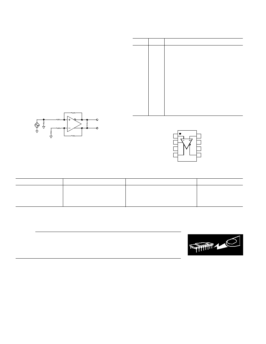
PIN CONFIGURATION
1
2
3
4
8
7
6
5
AD8138
NC
V
OCM
OUT
V+
NC = NO CONNECT
+IN
V
IN
+OUT
WARNING!
ESD SENSITIVE DEVICE
AD8138
R
F
= 499
R
G
= 499
R
G
= 499
24.9
R
L,dm
= 499
49.9
R
F
= 499
Figure 1. Basic Test Circuit
AD8138
5
REV. A
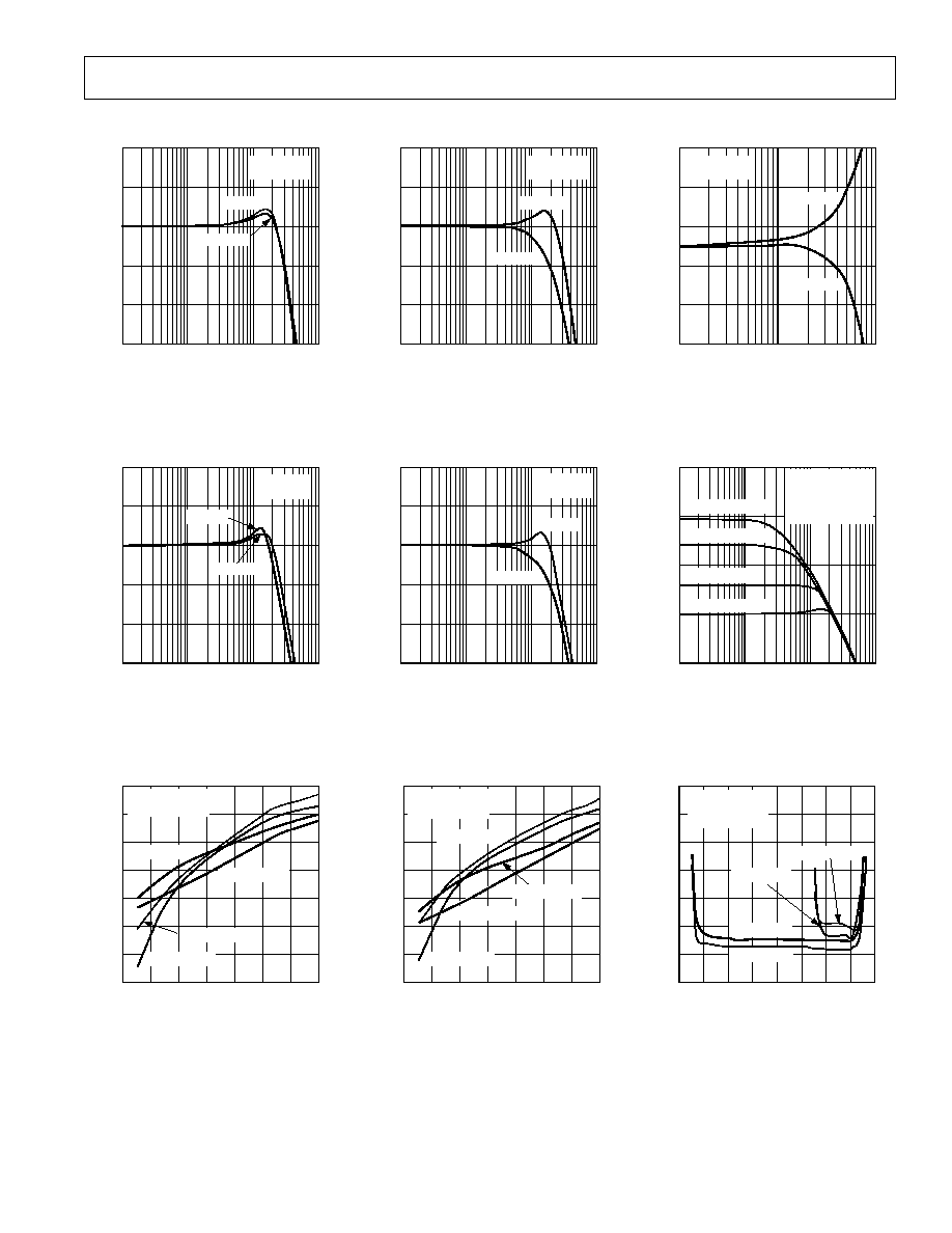
Typical Performance Characteristics
FREQUENCY MHz
GAIN dB
9
1
1000
0
10
100
6
3
3
6
V
S
= 5V
V
IN
= 0.2V p-p
C
F
= 0pF
V
S
= +5V
Figure 2. Small Signal Frequency
Response
FREQUENCY MHz
GAIN dB
9
1
1000
0
10
100
6
3
3
6
V
S
= 5V
V
IN
= 2V p-p
C
F
= 0pF
V
S
= +5V
Figure 5. Large Signal Frequency
Response
FUNDAMENTAL FREQUENCY MHz
0
10
70
20
30
40
50
60
DISTORTION dBc
50
120
90
100
110
70
80
HD2(V
S
= +5V)
60
HD2(V
S
= 5V)
V
OUT,dm
= 2V p-p
R
L
= 800
HD3(V
S
= +5V)
HD3(V
S
= 5V)
Figure 8. Harmonic Distortion vs.
Frequency
FREQUENCY MHz
GAIN dB
9
1
1000
0
10
100
6
3
3
6
C
F
= 1pF
V
S
= 5V
V
IN
= 0.2V p-p
C
F
= 0pF
Figure 3. Small Signal Frequency
Response
FREQUENCY MHz
GAIN dB
9
1
1000
0
10
100
6
3
3
6
C
F
= 1pF
V
IN
= 2V p-p
V
S
= 5V
C
F
= 0pF
Figure 6. Large Signal Frequency
Response
FUNDAMENTAL FREQUENCY MHz
0
10
70
20
30
40
50
60
DISTORTION dBc
50
90
100
110
70
80
HD2(V
S
= +5V)
60
HD2(V
S
= 5V)
V
OUT,dm
= 4V p-p
R
L
= 800
40
HD3(V
S
= 5V)
HD3(V
S
= +5V)
Figure 9. Harmonic Distortion vs.
Frequency
FREQUENCY MHz
GAIN dB
0.5
1
0.1
10
100
0.3
0.1
0.3
0.5
C
F
= 1pF
V
S
= 5V
V
IN
= 0.2V p-p
C
F
= 0pF
Figure 4. 0.1 dB Flatness vs.
Frequency
FREQUENCY MHz
GAIN dB
10
1
1000
10
10
100
0
V
S
= 5V
C
F
= 0pF
V
OUT,dm
= 0.2V p-p
R
G
= 499
G = 10, R
F
= 4.99k
20
30
G = 5, R
F
= 2.49k
G = 2, R
F
= 1k
G = 1, R
F
= 499
Figure 7. Small Signal Frequency
Response for Various Gains
V
OCM
DC OUTPUT Volts
4
3
3
2
1
0
1
2
DISTORTION dBc
50
90
100
70
80
60
HD2(V
S
= 5)
HD2(V
S
= +5)
V
OUT,dm
= 2V p-p
R
L
= 800
F
O
= 20MHz
40
30
4
HD3(V
S
= 5)
HD3(V
S
= +5)
Figure 10. Harmonic Distortion vs.
V
OCM
Unless otherwise noted, GAIN = 1, R
G
= R
F
= R
L,dm
= 499
, T
A
= +25 C; Refer to Figure 1 for test setup.