Äîêóìåíòàöèÿ è îïèñàíèÿ www.docs.chipfind.ru
REV. 0
Information furnished by Analog Devices is believed to be accurate and
reliable. However, no responsibility is assumed by Analog Devices for its
use, nor for any infringements of patents or other rights of third parties
which may result from its use. No license is granted by implication or
otherwise under any patent or patent rights of Analog Devices.
a
Fiber Optic Receiver with Quantizer and
Clock Recovery and Data Retiming
AD808
One Technology Way, P.O. Box 9106, Norwood, MA 02062-9106, U.S.A.
Tel: 781/329-4700
World Wide Web Site: http://www.analog.com
Fax: 781/326-8703
© Analog Devices, Inc., 1998
FEATURES
Meets CCITT G.958 Requirements
for STM-4 Regenerator--Type A
Meets Bellcore TR-NWT-000253 Requirements for OC-12
Output Jitter: 2.5 Degrees RMS
622 Mbps Clock Recovery and Data Retiming
Accepts NRZ Data, No Preamble Required
Phase-Locked Loop Type Clock Recovery--
No Crystal Required
Quantizer Sensitivity: 4 mV
Level Detect Range: 10 mV to 40 mV, Programmable
Single Supply Operation: +5 V or 5.2 V
Low Power: 400 mW
10 KH ECL/PECL Compatible Output
Package: 16-Lead Narrow 150 mil SOIC
frequency acquisition without false lock. This eliminates a reli-
ance on external components such as a crystal or a SAW filter,
to aid frequency acquisition.
The AD808 acquires frequency and phase lock on input data
using two control loops that work without requiring external
control. The frequency acquisition control loop initially acquires
the frequency of the input data, acquiring frequency lock on
random or scrambled data without the need for a preamble. At
frequency lock, the frequency error is zero and the frequency
detector has no further effect. The phase acquisition control
loop then works to ensure that the output phase tracks the input
phase. A patented phase detector has virtually eliminated pat-
tern jitter throughout the AD808.
The device VCO uses a ring oscillator architecture and patented
low noise design techniques. Jitter is 2.5 degrees rms. This low
jitter results from using a fully differential signal architecture,
Power Supply Rejection Ratio circuitry and a dielectrically
isolated process that provides immunity from extraneous signals
on the IC. The device can withstand hundreds of millivolts of
power supply noise without an effect on jitter performance.
The user sets the jitter peaking and acquisition time of the PLL
by choosing a damping factor capacitor whose value determines
loop damping. CCITT G.958 Type A jitter transfer require-
ments can easily be met with a damping factor of 5 or greater.
Device design guarantees that the clock output frequency will
drift by less than 20% in the absence of input data transitions.
Shorting the damping factor capacitor, C
D
, brings the clock
output frequency to the VCO center frequency.
The AD808 consumes 400 mW and operates from a single
power supply at either +5 V or 5.2 V.
FUNCTIONAL BLOCK DIAGRAM
SIGNAL
LEVEL
DETECTOR
COMPENSATING
ZERO
VCO
RETIMING
DEVICE
LOOP
FILTER
DET
PIN
NIN
THRADJ
SDOUT
CLKOUTP
CLKOUTN
DATAOUTP
DATAOUTN
LEVEL
DETECT
COMPARATOR/
BUFFER
AD808
PHASE-LOCKED LOOP
CF1
CF2
QUANTIZER
F
DET
PRODUCT DESCRIPTION
The AD808 provides the receiver functions of data quantiza-
tion, signal level detect, clock recovery and data retiming for
622 Mbps NRZ data. The device, together with a PIN
diode/preamplifier combination, can be used for a highly inte-
grated, low cost, low power SONET OC-12 or SDH STM-4
fiber optic receiver.
The receiver front end signal level detect circuit indicates when
the input signal level has fallen below a user adjustable thresh-
old. The threshold is set with a single external resistor. The
signal level detect circuit 3 dB optical hysteresis prevents chatter
at the signal level detect output.
The PLL has a factory trimmed VCO center frequency and a
frequency acquisition control loop that combine to guarantee
AD808SPECIFICATIONS
REV. 0
2
Parameter
Condition
Min
Typ
Max
Units
QUANTIZERDC CHARACTERISTICS
Input Voltage Range
@ P
IN
or N
IN
2.5
V
S
V
Input Sensitivity, V
SENSE
P
IN
N
IN
, Figure 1, BER =
1
×
10
10
10
4.0
mV
Input Overdrive, V
OD
Figure 1, BER =
1
×
10
10
5
2.0
mV
Input Offset Voltage
1.0
mV
Input Current
10
µ
A
Input RMS Noise
BER =
1
×
10
10
100
µ
V
Input Peak-to-Peak Noise
BER =
1
×
10
10
1.5
mV
QUANTIZERAC CHARACTERISTICS
Upper 3 dB Bandwidth
600
800
MHz
Input Resistance
10
k
Input Capacitance
2
pF
Pulsewidth Distortion
50
ps
LEVEL DETECT
Level Detect Range
R
THRESH
= 22.1 k
6.5
10
13.5
mV
R
THRESH
= 6.98 k
13
18
23
mV
R
THRESH
= 0
28.5
40
45.5
mV
Response Time
DC Coupled
0.1
1.5
µ
s
Hysteresis (Electrical)
R
THRESH
= 22.1 k
(See Figure 8)
5
9.0
dB
R
THRESH
= 6.98 k
3.0
5.1
9.0
dB
R
THRESH
= 0
3.0
7.0
10.0
dB
SDOUT Output Logic High
Load = +3.2 mA
4.0
4.7
V
SDOUT Output Logic Low
Load = 3.2 mA
0.2
0.4
V
PHASE-LOCKED LOOP NOMINAL
CENTER FREQUENCY
622.08
MHz
CAPTURE RANGE
620
624
MHz
TRACKING RANGE
620
624
MHz
STATIC PHASE ERROR (See Figure 7)
2
7
1 PRN Sequence
22
81
Degrees
SETUP TIME (t
SU
)
Figure 2
550
900
ps
HOLD TIME (t
H
)
Figure 2
700
1050
ps
PHASE DRIFT
240 Bits, No Transitions
50
Degrees
JITTER
2
7
1 PRN Sequence
2.5
3.6
Degrees rms
2
23
1 PRN Sequence
2.5
3.6
Degrees rms
JITTER TOLERANCE
f = 30 Hz
3000
Unit Intervals
f = 300 Hz
24
300
Unit Intervals
f = 25 kHz
1.7
3.7
Unit Intervals
f = 250 kHz
0.28
0.56
Unit Intervals
f = 5 MHz
0.18
0.45
Unit Intervals
JITTER TRANSFER
Peaking (Figure 14)
C
D
= 0.47
µ
F
0.04
dB
Bandwidth
333
450
kHz
Acquisition Time
C
D
= 0.1
µ
F
2
23
1 PRN Sequence, T
A
= +25
°
C
2
×
10
6
3
×
10
6
Bit Periods
C
D
= 0.47
µ
F
V
CC
= 5 V, V
EE
= GND
8
×
10
6
12
×
10
6
Bit Periods
POWER SUPPLY VOLTAGE
V
MIN
to V
MAX
4.5
5.5
Volts
POWER SUPPLY CURRENT
V
CC
= 5.0 V, V
EE
= GND,
T
A
= +25
°
C
55
80
100
mA
PECL OUTPUT VOLTAGE LEVELS
Output Logic High, V
OH
T
A
= +25
°
C
1.2
1.0
0.7
Volts
Output Logic Low, V
OL
Referenced to V
CC
2.2
2.0
1.7
Volts
SYMMETRY (Duty Cycle)
= 1/2, T
A
= +25
°
C,
Recovered Clock Output, Pin 5
V
CC
= 5 V, V
EE
= GND
45
55
%
OUTPUT RISE / FALL TIMES
Rise Time (t
R
)
20%80%
174
350
500
ps
Fall Time (t
F
)
80%20%
136
315
500
ps
CLOCK SKEW (t
RCS
)
Positive Number Indicates Clock
Leading Data
100
130
250
ps
Specifications subject to change without notice.
(T
A
= T
MIN
to T
MAX
, V
S
= V
MIN
to V
MAX
, C
D
= 0.47 F, unless otherwise noted)
AD808
REV. 0
3
ABSOLUTE MAXIMUM RATINGS
1
Supply Voltage . . . . . . . . . . . . . . . . . . . . . . . . . . . . . . . . . +8 V
Input Voltage (Pin 12 or Pin 13) . . . . . . . . . . . . . . V
CC
+ 0.6 V
Maximum Junction Temperature . . . . . . . . . . . . . . . . +165
°
C
Storage Temperature Range . . . . . . . . . . . . . 65
°
C to +150
°
C
Lead Temperature Range (Soldering 10 sec) . . . . . . . . +300
°
C
ESD Rating (Human Body Model) . . . . . . . . . . . . . . . . 1500 V
NOTES
1
Stresses above those listed under Absolute Maximum Ratings may cause perma-
nent damage to the device. This is a stress rating only; functional operation of the
device at these or any other conditions above those indicated in the operational
section of this specification is not implied. Exposure to absolute maximum rating
conditions for extended periods may affect device reliability.
Thermal Characteristics:
16-Lead Narrow Body SOIC Package:
JA
= 110
°
C/Watt.
NOISE
OFFSET
OVERDRIVE
SENSITIVITY
INPUT (V)
OUTPUT
1
0
Figure 1. Input Sensitivity, Input Overdrive
DATAOUT 50%
(PIN 2)
CLKOUT 50%
(PIN 5)
SETUP TIME
HOLD TIME
t
SU
t
H
RECOVERED
CLOCK SKEW
t
RCS
Figure 2. Setup and Hold Time
PIN FUNCTION DESCRIPTIONS
Pin
No.
Mnemonic
Description
1
DATAOUTN
Differential Retimed Data Output
2
DATAOUTP
Differential Retimed Data Output
3
V
CC2
Digital V
CC
for ECL Outputs
4
CLKOUTN
Differential Recovered Clock Output
5
CLKOUTP
Differential Recovered Clock Output
6
V
CC1
Digital V
CC
for Internal Logic
7
CF1
Loop Damping Capacitor
8
CF2
Loop Damping Capacitor
9
AV
EE
Analog V
EE
10
THRADJ
Level Detect Threshold Adjust
11
AV
CC1
Analog V
CC
for PLL
12
NIN
Quantizer Differential Input
13
PIN
Quantizer Differential Input
14
AV
CC2
Analog V
CC
for Quantizer
15
SDOUT
Signal Detect Output
16
V
EE
Digital V
EE
for Internal Logic
PIN CONFIGURATION
TOP VIEW
(Not to Scale)
16
15
14
13
12
11
10
9
1
2
3
4
5
6
7
8
DATAOUTN
DATAOUTP
V
CC2
CLKOUTN
CLKOUTP
V
CC1
CF1
CF2
V
EE
SDOUT
AV
CC2
PIN
NIN
AV
CC1
THRADJ
AV
EE
AD808
ORDERING GUIDE
Model
Temperature Range
Package Description
Package Option
AD808-622BR
40
°
C to +85
°
C
16-Pin Narrowbody SOIC
R-16A
AD808-622BRRL7
40
°
C to +85
°
C
750 Pieces, 7" Reel
R-16A
AD808-622BRRL
40
°
C to +85
°
C
2500 Pieces, 13" Reel
R-16A
CAUTION
ESD (electrostatic discharge) sensitive device. Electrostatic charges as high as 4000 V readily
accumulate on the human body and test equipment and can discharge without detection.
Although the AD808 features proprietary ESD protection circuitry, permanent damage may
occur on devices subjected to high energy electrostatic discharges. Therefore, proper ESD
precautions are recommended to avoid performance degradation or loss of functionality.
WARNING!
ESD SENSITIVE DEVICE

REV. 0
4
AD808
DEFINITION OF TERMS
Maximum, Minimum and Typical Specifications
Specifications for every parameter are derived from statistical
analyses of data taken on multiple devices from multiple wafer
lots. Typical specifications are the mean of the distribution of
the data for that parameter. If a parameter has a maximum (or a
minimum), that value is calculated by adding to (or subtracting
from) the mean six times the standard deviation of the distribu-
tion. This procedure is intended to tolerate production varia-
tions: if the mean shifts by 1.5 standard deviations, the remaining
4.5 standard deviations still provide a failure rate of only 3.4 parts
per million. For all tested parameters, the test limits are guard-
banded to account for tester variation to thus guarantee that no
device is shipped outside of data sheet specifications.
Input Sensitivity and Input Overdrive
Sensitivity and Overdrive specifications for the Quantizer in-
volve offset voltage, gain and noise. The relationship between
the logic output of the quantizer and the analog voltage input is
shown in Figure 1.
For sufficiently large positive input voltage the output is always
Logic 1 and similarly, for negative inputs, the output is always
Logic 0. However, the transitions between output Logic Levels
1 and 0 are not at precisely defined input voltage levels, but
occur over a range of input voltages. Within this Zone of Confu-
sion, the output may be either 1 or 0, or it may even fail to attain
a valid logic state. The width of this zone is determined by the
input voltage noise of the quantizer (1.5 mV at the 1
×
10
10
confidence level). The center of the Zone of Confusion is the
quantizer input offset voltage (1 mV typ). Input Overdrive is the
magnitude of signal required to guarantee correct logic level
with 1
×
10
10
confidence level.
With a single-ended PIN-TIA (Figure 3), ac coupling is used
and the inputs to the Quantizer are dc biased at some common-
mode potential. Observing the Quantizer input with an oscillo-
scope probe at the point indicated shows a binary signal with
average value equal to the common-mode potential and instan-
taneous values both above and below the average value. It is
convenient to measure the peak-to-peak amplitude of this signal
and call the minimum required value the Quantizer Sensitivity.
Referring to Figure 1, since both positive and negative offsets
need to be accommodated, the Sensitivity is twice the Over-
drive. The AD808 Quantizer has 4 mV Sensitivity typical.
With a differential TIA (Figure 3), Sensitivity seems to improve
from observing the Quantizer input with an oscilloscope probe.
This is an illusion caused by the use of a single-ended probe. A
2 mV peak-to-peak signal appears to drive the AD808 Quan-
tizer. However, the single-ended probe measures only half the
signal. The true Quantizer input signal is twice this value since
the other Quantizer input is a complementary signal to the sig-
nal being observed.
Response Time
Response time is the delay between removal of the input signal
and indication of Loss of Signal (LOS) at SDOUT. The re-
sponse time of the AD808 (1.5
µ
s maximum) is much faster
than the SONET/SDH requirement (3
µ
s
response time
100
µ
s). In practice, the time constant of the ac coupling at the
Quantizer input determines the LOS response time.
Nominal Center Frequency
This is the frequency at which the VCO will oscillate with the
loop damping capacitor, C
D
, shorted.
Tracking Range
This is the range of input data rates over which the AD808 will
remain in lock.
Capture Range
This is the range of input data rates over which the AD808 will
acquire lock.
Static Phase Error
This is the steady-state phase difference, in degrees, between the
recovered clock sampling edge and the optimum sampling in-
stant, which is assumed to be halfway between the rising and
falling edges of a data bit. Gate delays between the signals that
define static phase error, and IC input and output signals pro-
hibit direct measurement of static phase error.
Data Transition Density,
This is a measure of the number of data transitions, from "0" to
"1" and from "1" to "0," over many clock periods.
is the ratio
(0
1) of data transitions to bit periods.
Jitter
This is the dynamic displacement of digital signal edges from
their long term average positions, measured in degrees rms or
Unit Intervals (UI). Jitter on the input data can cause dynamic
phase errors on the recovered clock sampling edge. Jitter on the
recovered clock causes jitter on the retimed data.
Output Jitter
This is the jitter on the retimed data, in degrees rms, due to a
specific pattern or some pseudorandom input data sequence
(PRN Sequence).
Jitter Tolerance
Jitter Tolerance is a measure of the AD808's ability to track a
jittery input data signal. Jitter on the input data is best thought
of as phase modulation, and is usually specified in unit intervals.
The PLL must provide a clock signal that tracks the phase
modulation in order to accurately retime jittered data. In order
for the VCO output to have a phase modulation that tracks the
input jitter, some modulation signal must be generated at the
output of the phase detector. The modulation output from the
phase detector can only be produced by a phase error between
its data input and its clock input. Hence, the PLL can never
perfectly track jittered data. However, the magnitude of the
phase error depends on the gain around the loop. At low fre-
quencies, the integrator of the AD808 PLL provides very high
gain, and thus very large jitter can be tracked with small phase
errors between input data and recovered clock. At frequencies
closer to the loop bandwidth, the gain of the integrator is much
smaller, and thus less input jitter can be tolerated. The AD808
output will have a bit error rate less than 1
×
10
10
when in lock
and retiming input data that has the CCITT G.958 specified
jitter applied to it.
Jitter Transfer (Refer to Figure 14)
The AD808 exhibits a low-pass filter response to jitter applied
to its input data.
Bandwidth
This describes the frequency at which the AD808 attenuates
sinusoidal input jitter by 3 dB.
Peaking
This describes the maximum jitter gain of the AD808 in dB.
AD808
REV. 0
5
Damping Factor,
Damping factor,
describes the compensation of the second
order PLL. A larger value of
corresponds to more damping
and less peaking in the jitter transfer function.
Acquisition Time
This is the transient time, measured in bit periods, required for
the AD808 to lock onto input data from its free-running state.
Symmetry--Recovered Clock Duty Cycle
Symmetry is calculated as (100
×
on time)/period, where on
time equals the time that the clock signal is greater than the
midpoint between its "0" level and its "1" level.
BINARY
OUTPUT
SCOPE
PROBE
AD808 QUANTIZER
V
CM
V
CM
4mVp-p
INPUT
a. Single-Ended Input Application
BINARY
OUTPUT
SCOPE
PROBE
AD808 QUANTIZER
V
CM
V
CM
2mVp-p
+INPUT
INPUT
b. Differential Input Application
Figure 3. (ab) Single-Ended and Differential Input
Applications
500
500
5k
5k
AV
EE
AV
CC
OUT
PIN
NIN
a. Quantizer Differential Input Stage
6k
THRADJ
AV
EE
80k
1.2V +V
BE
b. Threshold Adjust
30
V
CC1
SDOUT
V
EE
I
OL
I
OH
30
c. Signal Detect Output (SDOUT)
140
140
V
CC2
DIFFERENTIAL
OUTPUT
V
EE
7.8mA
d. PLL Differential Output Stage--DATAOUT(N),
CLKOUT(N)
Figure 4. (ad) Simplified Schematics
The AD808 has internal circuits to set the common-mode volt-
age at the quantizer inputs PIN (Pin 13) and NIN (Pin 12) as
shown in Figure 4a. This allows very simple capacitive coupling
of the signal from the preamp in the AD808 as shown in Figure
3. The internal common-mode potential is a diode drop (ap-
proximately 0.8 V) below the positive supply as shown in Figure
4a. Since the common mode is referred to the positive supply, it
is useful to bypass the common mode of the preamp to the
positive supply as well, if this is an option. Note, it is not neces-
sary to use capacitive coupling of the input signal with the
AD808. Figure 14 shows the input common-mode voltage can
be externally set.
AD808Typical Performance Characteristics
90000
80000
0
R
THRESH
40000
30000
20000
10000
60000
50000
70000
SIGNAL DETECT VOLTAGE mV
16
6
8
10
12
14
4
Figure 5. Signal Detect Voltage vs. R
THRESH
TEMPERATURE C
40
95
20
0
20
40
60
80
8.0
4.0
ELECTRICAL HYSTERESIS dB
7.5
6.0
5.5
5.0
4.5
7.0
6.5
R
TH
= 5k
R
TH
= 7k
R
TH
= 0
Figure 6. Signal Detect Hysteresis vs. Temperature
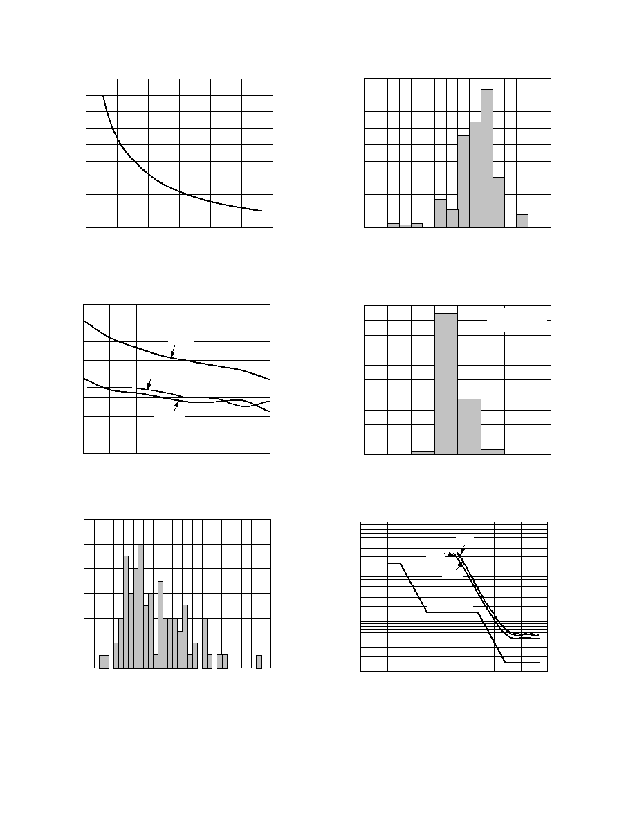
STATIC PHASE Degrees
0
0
8
SAMPLES
17
25
33
42
50
58
12
8
2
10
6
4
Figure 7. Histogram of Static Phase 40 @ 4.4 V
REV. 0
6
LOS HYSTERESIS dB
0
2.00
2.67
SAMPLES
3.33
4.00
4.67
5.33
6.00
6.67
180
120
80
40
20
160
140
100
60
Figure 8. Histogram LOS Hysteresis 22.1 k
R
THRESH
(All Temperature All Supply)
JITTER Degrees
200
0
1.44
1.80
SAMPLES
2.16
2.52
2.88
3.24
3.60
3.96
180
120
80
40
20
160
140
100
60
TEST CONDITIONS
WORST CASE:
40 C
Figure 9. Output Jitter Histogram
JITTER FREQUENCY Hz
100
10
0.1
1
10M
10
JITTER TOLERANCE UI
100
1k
10k
100k
1M
1
SONET MASK
85 C
25 C
40 C
Figure 10. Jitter Tolerance vs. Frequency
AD808
REV. 0
7
THEORY OF OPERATION
Quantizer
The quantizer (comparator) has three gain stages, providing a
net gain of 350. The quantizer takes full advantage of the Extra
Fast Complementary Bipolar (XFCB) process. The input stage
uses a folded cascode architecture to virtually eliminate pulse
width distortion, and to handle input signals with common-
mode voltage as high as the positive supply. The input offset
voltage is factory trimmed and is typically less than 1 mV. XFCB's
dielectric isolation allows the different blocks within this mixed-
signal IC to be isolated from each other, hence the 4 mV Sensi-
tivity is achieved. Traditionally, high speed comparators are
plagued by crosstalk between outputs and inputs, often resulting
in oscillations when the input signal approaches 10 mV. The
AD808 quantizer toggles at 2 mV (4.0 mV sensitivity) at the
input without making bit errors. When the input signal is low-
ered below 2 mV, circuit performance is dominated by input
noise, and not crosstalk.
Signal Detect
The input to the signal detect circuit is taken from the first stage
of the quantizer. The input signal is first processed through a
gain stage. The output from the gain stage is fed to both a posi-
tive and a negative peak detector. The threshold value is sub-
tracted from the positive peak signal and added to the negative
peak signal. The positive and negative peak signals are then
compared. If the positive peak, POS, is more positive than the
negative peak, NEG, the signal amplitude is greater than the
threshold, and the output, SDOUT, will indicate the presence
of signal by remaining low. When POS becomes more negative
than NEG, the signal amplitude has fallen below the threshold,
and SDOUT will indicate a loss of signal (LOS) by going high.
The circuit provides hysteresis by adjusting the threshold level
higher by a factor of two when the low signal level is detected.
This means that the input data amplitude needs to reach twice
the set LOS threshold before SDOUT will signal that the data is
again valid. This corresponds to a 3 dB optical hysteresis.
POSITIVE
PEAK
DETECTOR
NEGATIVE
PEAK
DETECTOR
LEVEL
SHIFT
DOWN
LEVEL
SHIFT
UP
THRESHOLD
BIAS
PIN
NIN
SDOUT
IHYS
+
+
AD808
COMPARATOR STAGES
& CLOCK RECOVERY PLL
ITHR
Figure 11. Signal Level Detect Circuit Block Diagram
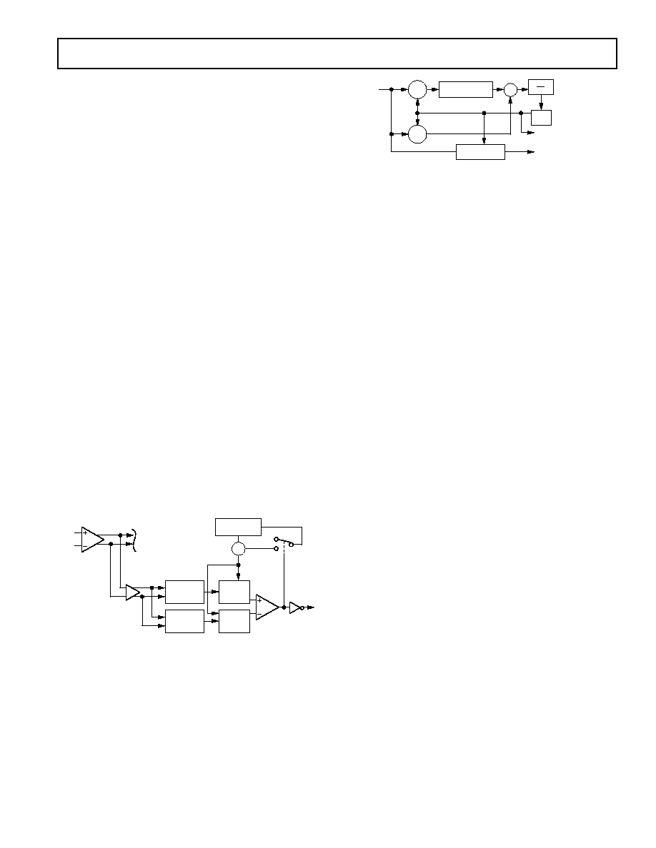
Phase-Locked Loop
The phase-locked loop recovers clock and retimes data from
NRZ data. The architecture uses a frequency detector to aid
initial frequency acquisition; refer to Figure 12 for a block dia-
gram. Note the frequency detector is always in the circuit. When
the PLL is locked, the frequency error is zero and the frequency
detector has no further effect. Since the frequency detector is
always in the circuit, no control functions are needed to initiate
acquisition or change mode after acquisition.
VCO
RETIMING
DEVICE
DET
F
DET
DATA
INPUT
1
S
S + 1
RECOVERED CLOCK
OUTPUT
RETIMED DATA
OUTPUT
Figure 12. PLL Block Diagram
The frequency detector delivers pulses of current to the charge
pump to either raise or lower the frequency of the VCO. During
the frequency acquisition process the frequency detector output
is a series of pulses of width equal to the period of the VCO.
These pulses occur on the cycle slips between the data fre-
quency and the VCO frequency. With a maximum density data
pattern (1010 . . . ), every cycle slip will produce a pulse at the
frequency detector output. However, with random data, not
every cycle slip produces a pulse. The density of pulses at the
frequency detector output increases with the density of data
transitions. The probability that a cycle slip will produce a pulse
increases as the frequency error approaches zero. After the fre-
quency error has been reduced to zero, the frequency detector
output will have no further pulses. At this point the PLL begins
the process of phase acquisition, with a settling time of roughly
2000 bit periods.
Jitter caused by variations of density of data transitions (pattern
jitter) is virtually eliminated by use of a new phase detector
(patented). Briefly, the measurement of zero phase error does
not cause the VCO phase to increase to above the average run
rate set by the data frequency. The jitter created by a 2
7
1 pseu-
dorandom code is 1/2 degree, and this is small compared to
random jitter.
The jitter bandwidth for the PLL is 0.06% of the center fre-
quency. This figure is chosen so that sinusoidal input jitter at
350 Hz will be attenuated by 3 dB.
The damping ratio of the PLL is user programmable with a
single external capacitor. At 622 MHz, a damping ratio of 5 is
obtained with a 0.47
µ
F capacitor. More generally, the damping
ratio scales as (f
DATA
×
C
D
)
1/2
.
A lower damping ratio allows a faster frequency acquisition;
generally the acquisition time scales directly with the capacitor
value. However, at damping ratios approaching one, the acquisi-
tion time no longer scales directly with capacitor value. The
acquisition time has two components: frequency acquisition and
phase acquisition. The frequency acquisition always scales with
capacitance, but the phase acquisition is set by the loop band-
width of the PLL and is independent of the damping ratio. In
practice the acquisition time is dominated by the frequency
acquisition. The fractional loop bandwidth of 0.06% should
give an acquisition time of 2000 bit periods. However, the
actual acquisition time is several million bit periods and is
comprised mostly of the time needed to slew the voltage on
the damping capacitor to final value.
REV. 0
8
AD808
1
2
5
6
7
3
4
8
V
EE
SDOUT
NIN
AV
CC1
THRADJ
AV
EE
AD808
PIN
16
15
12
11
10
14
13
9
R10
154
R9
154
R6 100
C7
R5 100
R1
100
R2
100
C1 0.1 F
DATAOUTN
DATAOUTP
CLKOUTN
CLKOUTP
C5 0.1 F
C2
0.1 F
R4
100
R8 100
R7 100
R3
100
C8
R12
154
TP1
TP2
R11
154
CD
TP7
SDOUT
TP5
TP6
R
THRESH
C11
10 F
C10
GND
R14
49.9
R15
49.9
C12
0.1 F
C4 0.1 F
C3 0.1 F
C6
0.1 F
J1
J2
J3
J4
+5V
TP3
TP4
NOTE: INTERCONNECT RUN
UNDER DUT
VECTOR PINS SPACED FOR RN55C
TYPE RESISTOR; COMPONENT
SHOWN FOR REFERENCE ONLY
VECTOR PINS SPACED THROUGH-HOLE
CAPACITOR ON VECTOR CUPS; COMPONENT
SHOWN FOR REFERENCE ONLY
TP8
J5
C9
R13
301
R16 3.65k
J6
J7
C13 0.1 F
C14 0.1 F
PIN
NIN
50 STRIP LINE
EQUAL LENGTH
NOTE:
C7C10 ARE 0.1µF BYPASS CAPACITORS
RIGHT ANGLE SMA CONNECTOR
OUTER SHELL TO GND PLANE
ALL RESISTORS ARE 1% 1/8 WATT SURFACE MOUNT
TPxo TEST POINTS ARE VECTORBOARD K24A/M PINS
DATAOUTN
DATAOUTP
V
CC2
CLKOUTN
CLKOUTP
V
CC1
CF1
CF2
AV
CC2
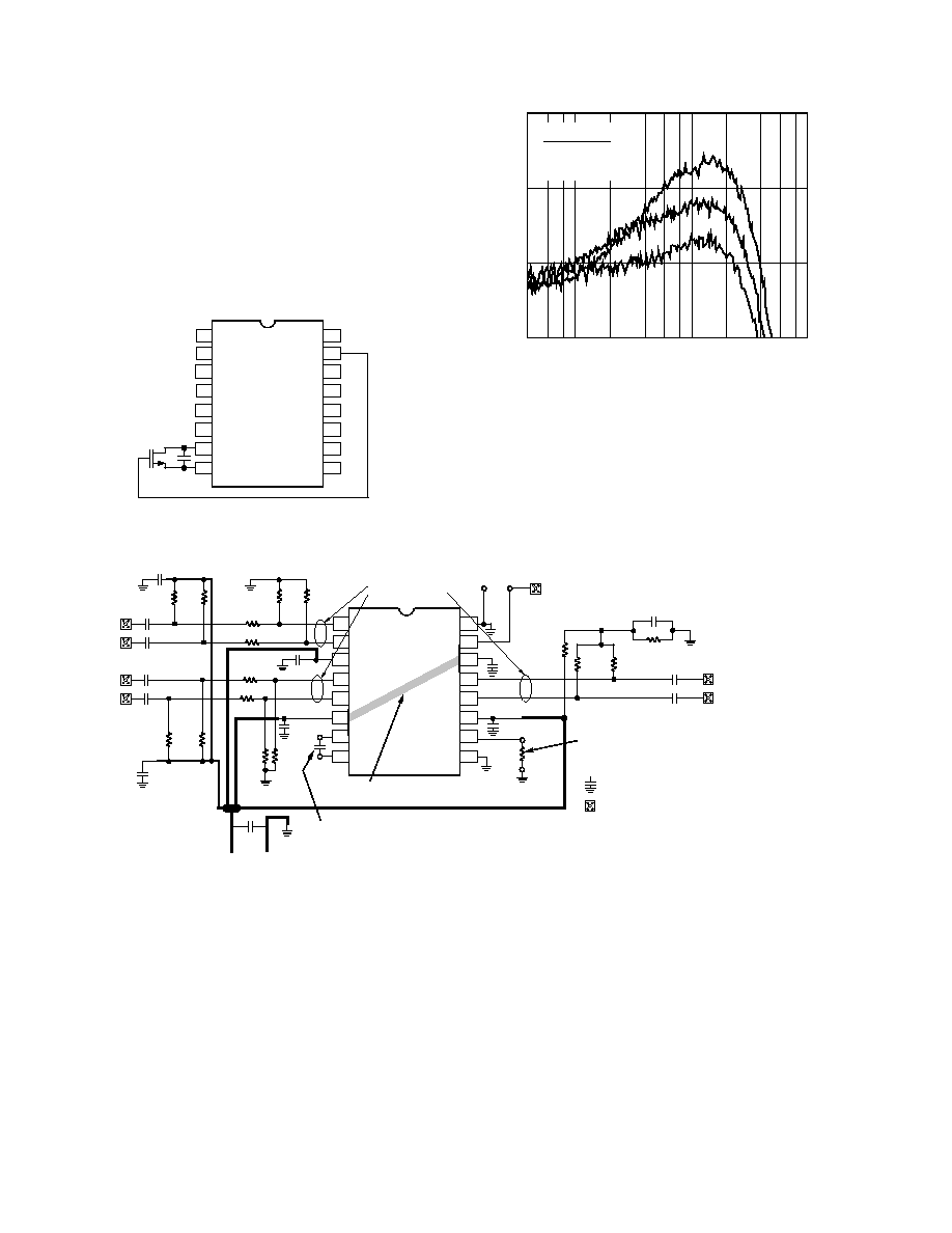
Figure 15. Evaluation Board Schematic
Center Frequency Clamp (Figure 13)
An N-channel FET circuit can be used to bring the AD808
VCO center frequency to within
±
10% of 622 MHz when
SDOUT indicates a Loss of Signal (LOS). This effectively re-
duces the frequency acquisition time by reducing the frequency
error between the VCO frequency and the input data frequency
at clamp release. The N-FET can have "on" resistance as high
as 1 k
and still attain effective clamping. However, the chosen
N-FET should have greater than 10 M
"off" resistance and
less than 100 nA leakage current (source and drain) so as not to
alter normal PLL performance.
1
2
5
6
7
3
4
8
16
15
12
11
10
14
13
9
V
EE
SDOUT
AV
CC2
PIN
NIN
AV
CC1
THRADJ
AV
EE
DATAOUTN
DATAOUTP
CLKOUTN
CLKOUTP
V
CC1
CF1
CF2
V
CC2
AD808
N_FET
C
D
Figure 13. Center Frequency Clamp Schematic
RBW:
30Hz ST: 3.07 min RANGE: R=
0, T=
0dBm
DIV
20.00m
C
D
PEAK
0.047
0.11
0.10
0.07
0.47
0.04
DIV
36.00m
START
STOP
500.000Hz
100 000.000Hz
Figure14. Jitter Transfer vs. C
D
AD808
REV. 0
9
USING THE AD808
Acquisition Time
This is the transient time, measured in bit periods, that required
for the AD808 to lock onto the input data from its free running
state.
Ground Planes
The use of one ground plane for connections to both analog and
digital grounds is recommended.
Power Supply Connections
The use of a 10
µ
F capacitor between V
CC
and ground is recom-
mended. The +5 V power supply connection to V
CC2
should be
carefully isolated. The V
CC2
pin is used inside the AD808 to
provide the CLKOUT and DATAOUT signals.
Use a 0.1
µ
F decoupling capacitor between IC power supply
input and ground. This decoupling capacitor should be posi-
tioned as closed to the IC as possible. Refer to the schematic in
Figure 15 for advised connections.
Transmission Lines
Use 50
transmission line for PIN, NIN, CLKOUT, and
DATAOUT signals.
Terminations
Use metal, thick-film, 1% termination resistors for PIN, NIN,
CLKOUT, and DATAOUT signals. These termination resistors
must be positioned as close to the IC as possible.
Use individual connections, not daisy chained, for connections
from the +5 V to load resistors for PIN, NIN, CLKOUT, and
DATAOUT signals.
Loop Damping Capacitor, C
D
A ceramic capacitor may be used for the loop damping capaci-
tor. Using a 0.47
µ
F,
±
20% capacitor provides < 0.1 dB jitter
peaking.
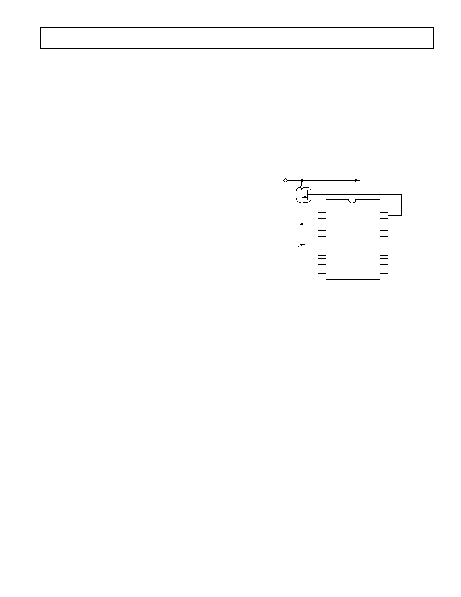
AD808 Output Squelch Circuit
A simple P-channel FET circuit can be used in series with the
Output Signal ECL Supply (V
CC2
, Pin 3) to squelch clock and
data outputs when SDOUT indicates a loss of signal (Figure
16). The V
CC2
supply pin draws roughly 72 mA (14 mA for each
of 4 ECL loads, plus 16 mA for all 4 ECL output stages). This
means that selection of a FET with ON RESISTANCE of
0.5
will affect the common mode of the ECL outputs by
only 36 mV.
1
2
5
6
7
3
4
8
16
15
12
11
10
14
13
9
V
EE
SDOUT
AV
CC2
PIN
NIN
AV
CC1
THRADJ
AV
EE
DATAOUTN
DATAOUTP
CLKOUTN
CLKOUTP
V
CC1
CF1
CF2
V
CC2
AD808
TO V
CC1
, AV
CC
, AV
CC2
P_FET
BYPASS
CAP
5V
Figure 16. Squelch Circuit Schematic
REV. 0
10
AD808
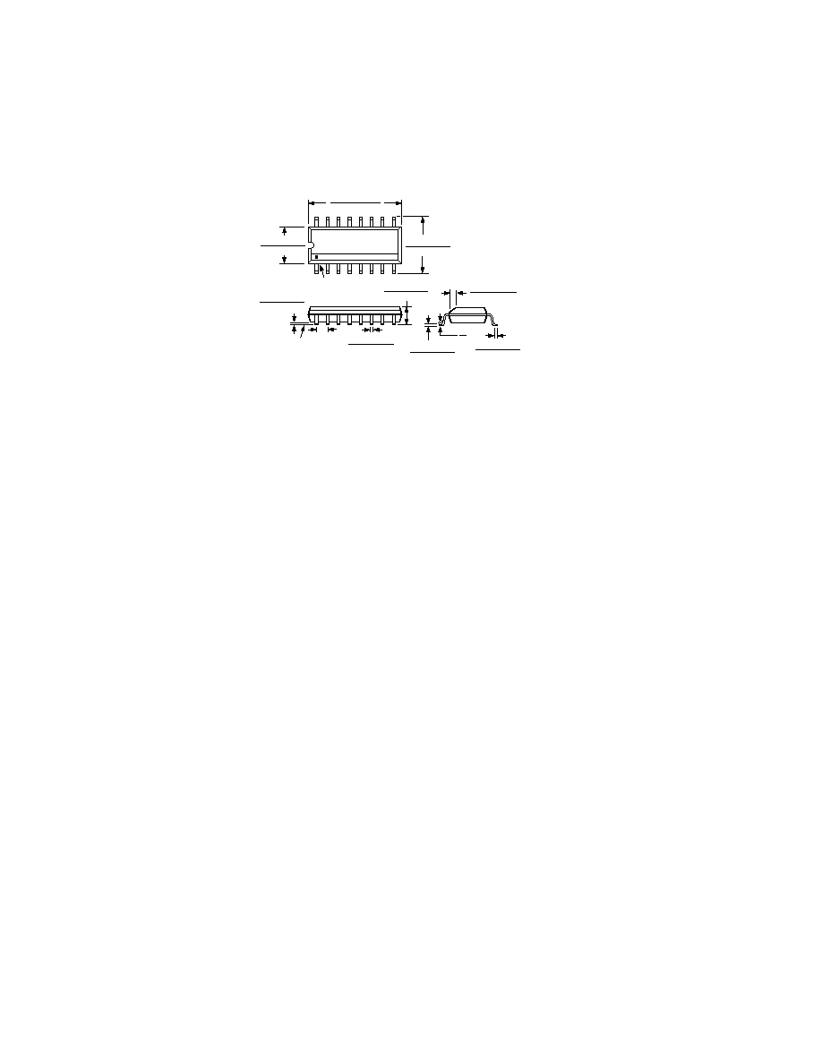
OUTLINE DIMENSIONS
Dimensions shown in inches and (mm).
16-Lead Small Outline IC Package
(R-16A)
16
9
8
1
0.3937 (10.00)
0.3859 (9.80)
0.2440 (6.20)
0.2284 (5.80)
0.1574 (4.00)
0.1497 (3.80)
PIN 1
SEATING
PLANE
0.0098 (0.25)
0.0040 (0.10)
0.0192 (0.49)
0.0138 (0.35)
0.0688 (1.75)
0.0532 (1.35)
0.0500
(1.27)
BSC
0.0099 (0.25)
0.0075 (0.19)
0.0500 (1.27)
0.0160 (0.41)
8
0
0.0196 (0.50)
0.0099 (0.25)
x 45

11

PRINTED IN U.S.A.
C326281/98
12