Äîêóìåíòàöèÿ è îïèñàíèÿ www.docs.chipfind.ru
FUNCTIONAL BLOCK DIAGRAM
VCO
DATA
INPUT
AD800/AD802
C
D
RETIMED
DATA
OUTPUT
FRAC
OUTPUT
LOOP
FILTER
Ø
DET
f
DET
COMPENSATING
ZERO
RECOVERED
CLOCK
OUTPUT
RETIMING
DEVICE
REV. B
Information furnished by Analog Devices is believed to be accurate and
reliable. However, no responsibility is assumed by Analog Devices for its
use, nor for any infringements of patents or other rights of third parties
which may result from its use. No license is granted by implication or
otherwise under any patent or patent rights of Analog Devices.
a
Clock Recovery and Data Retiming
Phase-Locked Loop
AD800/AD802*
One Technology Way, P.O. Box 9106, Norwood, MA 02062-9106, U.S.A.
Tel: 617/329-4700
Fax: 617/326-8703
PRODUCT DESCRIPTION
The AD800 and AD802 employ a second order phase-locked
loop architecture to perform clock recovery and data retiming
on Non-Return to Zero, NRZ, data. This architecture is
capable of supporting data rates between 20 Mbps and 160
Mbps. The products described here have been defined to work
with standard telecommunications bit rates. 45 Mbps DS-3 and
52 Mbps STS-1 are supported by the AD800-45 and
AD800-52 respectively. 155 Mbps STS-3 or STM-1 are
supported by the AD802-155.
Unlike other PLL-based clock recovery circuits, these devices
do not require a preamble or an external VCXO to lock onto
input data. The circuit acquires frequency and phase lock using
two control loops. The frequency acquisition control loop
initially acquires the clock frequency of the input data. The
phase-lock loop then acquires the phase of the input data, and
ensures that the phase of the output signals track changes in the
phase of the input data. The loop damping of the circuit is
dependent on the value of a user selected capacitor; this defines
jitter peaking performance and impacts acquisition time. The
devices exhibit 0.08 dB jitter peaking, and acquire lock on
random or scrambled data within 4
×
10
5
bit periods when
using a damping factor of 5.
FEATURES
Standard Products
44.736 Mbps--DS-3
51.84 Mbps--STS-1
155.52 Mbps--STS-3 or STM-1
Accepts NRZ Data, No Preamble Required
Recovered Clock and Retimed Data Outputs
Phase-Locked Loop Type Clock Recovery--No Crystal
Required
Random Jitter: 20 Peak-to-Peak
Pattern Jitter: Virtually Eliminated
10KH ECL Compatible
Single Supply Operation: 5.2 V or +5 V
Wide Operating Temperature Range: 40 C to +85 C
During the process of acquisition the frequency detector
provides a Frequency Acquisition (FRAC) signal which
indicates that the device has not yet locked onto the input data.
This signal is a series of pulses which occur at the points of cycle
slip between the input data and the synthesized clock signal.
Once the circuit has acquired frequency lock no pulses occur at
the FRAC output.
The inclusion of a precisely trimmed VCO in the device
eliminates the need for external components for setting center
frequency, and the need for trimming of those components. The
VCO provides a clock output within
±
20% of the device center
frequency in the absence of input data.
The AD800 and AD802 exhibit virtually no pattern jitter, due
to the performance of the patented phase detector. Total loop
jitter is 20
°
peak-to-peak. Jitter bandwidth is dictated by mask
programmable fractional loop bandwidth. The AD800, used for
data rates < 90 Mbps, has been designed with a nominal loop
bandwidth of 0.1% of the center frequency. The AD802, used
for data rates in excess of 90 Mbps, has a loop bandwidth of
0.08% of center frequency.
All of the devices operate with a single +5 V or 5.2 V supply.
*Protected by U.S. Patent No. 5,027,085.
REV. B
2
AD800/AD802SPECIFICATIONS
(V
EE
= V
MIN
to V
MAX
, V
CC
= GND, T
A
= T
MIN
to T
MAX
, Loop Damping
Factor = 5, unless otherwise noted)
AD800-45BQ
AD800-52BR
AD802-155KR/BR
Parameter
1
Condition
Min
Typ
Max
Min
Typ
Max
Min
Typ
Max
Units
NOMINAL CENTER FREQUENCY
44.736
51.84
155.52
MHz
OPERATING TEMPERATURE
K Grade
0
70
°
C
RANGE (T
MIN
to T
MAX
)
B Grade
40
85
40
85
40
85
°
C
TRACKING RANGE
43
45.5
49
53
155
156
Mbps
CAPTURE RANGE
43
45.5
49
53
155
156
Mbps
STATIC PHASE ERROR
= 1, T
A
= +25
°
C,
V
EE
= 5.2 V
2
10
2
10
14
30
Degrees
= 1
3
11.5
3
11.5
18
37
Degrees
RECOVERED CLOCK SKEW
t
RCS
(Figure 1)
0.2
0.6
1
0.2
0.6
1
0.2
0.8
1
ns
SETUP TIME
t
SU
(Figure 1)
2.06
2.37
ns
TRANSITIONLESS DATA RUN
240
240
240
Bit Periods
OUTPUT JITTER
= 1
2
2
3.5
Degrees rms
2
7
1 PRN Sequence
2.5
4.7
2.5
4.7
5.4
9.7
Degrees rms
2
23
1 PRN Sequence
2.5
4.7
2.5
4.7
5.4
9.7
Degrees rms
JITTER TOLERANCE
f = 10 Hz
2,500
2,500
3,000
Unit Intervals
f = 2.3 kHz
6.5
Unit Intervals
f = 30 kHz
0.47
Unit Intervals
f = 1 MHz
0.47
Unit Intervals
f = 30 Hz
830
Unit Intervals
f = 300 Hz
83
Unit Intervals
f = 2 kHz
7.4
Unit Intervals
f = 20 kHz
0.47
Unit Intervals
f = 6.5 kHz
2.0
7.6
Unit Intervals
f = 65 kHz
0.26
0.9
Unit Intervals
JITTER TRANSFER
Damping Factor
Capacitor, C
D
= 1, Nominal
8.2
6.8
2.2
nF
= 5, Nominal
0.22
0.15
0.047
µ
F
= 10, Nominal
0.82
0.68
0.22
µ
F
Peaking
= 1, Nominal
T
A
= +25
°
C, V
EE
= 5.2 V
2
2
2
dB
= 5, Nominal
T
A
= +25
°
C, V
EE
= 5.2 V
0.08
0.08
0.08
dB
= 10, Nominal
T
A
= +25
°
C, V
EE
= 5.2 V
0.02
0.02
0.02
dB
Bandwidth
45
52
130
kHz
ACQUISITION TIME
= 1/2
= 1
1
×
10
4
1
×
10
4
1.5
×
10
4
Bit Periods
T
A
= +25
°
C
= 5
3
×
10
5
8
×
10
5
3
×
10
5
8
×
10
5
4
×
10
5
8
×
10
5
Bit Periods
V
EE
= 5.2 V
= 10
8
×
10
5
8
×
10
5
1.4
×
10
6
Bit Periods
POWER SUPPLY
Voltage (V
MIN
to V
MAX
)
T
A
= +25
°
C
4.5
5.2
5.5
4.5
5.2
5.5
4.5
5.2
5.5
Volts
Current
T
A
= +25
°
C, V
EE
= 5.2 V
125
170
125
170
140
180
mA
180
180
205
mA
INPUT VOLTAGE LEVELS
T
A
= +25
°
C
Input Logic High, V
IH
1.084
0.72
1.084
0.72
1.084
0.72
Volts
Input Logic Low, V
IH
1.95
1.594
1.95
1.594
1.95
1.594
Volts
OUTPUT VOLTAGE LEVELS
T
A
= +25
°
C
Output Logic High, V
OH
1.084
0.72
1.084
0.72
1.084
0.72
Volts
Output Logic Low, V
OL
1.95
1.60
1.95
1.60
1.95
1.60
Volts
INPUT CURRENT LEVELS
T
A
= +25
°
C
Input Logic High, I
IH
125
125
125
µ
A
Input Logic Low, I
IL
80
80
80
µ
A
OUTPUT SLEW TIMES
T
A
= +25
°
C
Rise Time (t
R
)
20%80%
0.75
1.5
0.75
1.5
0.75
1.5
ns
Fall Time (t
F
)
80%20%
0.75
1.5
0.75
1.5
0.75
1.5
ns
SYMMETRY
= 1/2, T
A
= +25
°
C
Recovered Clock Output
V
EE
= 5.2 V
45
55
45
55
45
55
%
NOTES
1
Refer to Glossary for parameter definition.
Specifications subject to change without notice.
AD800/AD802
REV. B
3
ABSOLUTE MAXIMUM RATINGS*
Supply Voltage . . . . . . . . . . . . . . . . . . . . . . . . . . . . . . . . . 6 V
Input Voltage (Pin 16 or Pin 17 to V
CC
) . . . . V
EE
to +300 mV
Maximum Junction Temperature
SOIC Package . . . . . . . . . . . . . . . . . . . . . . . . . . . . .+150
°
C
Ceramic DIP Package . . . . . . . . . . . . . . . . . . . . . . +175
°
C
Storage Temperature Range . . . . . . . . . . . . 65
°
C to +150
°
C
Lead Temperature Range (Soldering 60 sec) . . . . . . . +300
°
C
ESD Rating
AD800 . . . . . . . . . . . . . . . . . . . . . . . . . . . . . . . . . . . 1500 V
AD802 . . . . . . . . . . . . . . . . . . . . . . . . . . . . . . . . . . . 1000 V
*Stresses above those listed under "Absolute Maximum Ratings" may cause
permanent damage to the device. This is a stress rating only; functional operation
of the device at these or any other conditions above those indicated in the
operational section of this specification is not implied. Exposure to an absolute
maximum rating condition for an extended period may adversely affect device
reliability.
RECOVERED CLOCK
SKEW,
t
RCS
DATAOUT 50%
(PIN 2)
CLKOUT 50%
(PIN 5)
SETUP TIME
t
SU
Figure 1. Recovered Clock Skew and Setup
(See Previous Page)
PIN DESCRIPTIONS
Number
Mnemonic
Description
1
DATAOUT
Differential Retimed Data Output
2
DATAOUT
Differential Retimed Data Output
3
V
CC2
Digital Ground
4
CLKOUT
Differential Recovered Clock Output
5
CLKOUT
Differential Recovered Clock Output
6
V
EE
Digital V
EE
7
V
EE
Digital V
EE
8
V
CC1
Digital Ground
9
AV
EE
Analog V
EE
10
ASUBST
Analog Substrate
11
CF
2
Loop Damping Capacitor Input
12
CF
1
Loop Damping Capacitor Input
13
AV
CC
Analog Ground
14
V
CC1
Digital Ground
15
V
EE
Digital V
EE
16
DATAIN
Differential Data Input
17
DATAIN
Differential Data Input
18
SUBST
Digital Substrate
19
FRAC
Differential Frequency Acquisition
Indicator Output
20
FRAC
Differential Frequency Acquisition
Indicator Output
THERMAL CHARACTERISTICS
JC
JA
SOIC Package
22
°
C/W
75
°
C/W
Cerdip Package
25
°
C/W
90
°
C/W
Use of a heatsink may be required depending on operating
environment.
GLOSSARY
Maximum and Minimum Specifications
Maximum and minimum specifications result from statistical
analyses of measurements on multiple devices and multiple test
systems. Typical specifications indicate mean measurements.
Maximum and minimum specifications are calculated by adding
or subtracting an appropriate guardband from the typical
specification. Device-to-device performance variation and test
system-to-test system variation contribute to each guardband.
Nominal Center Frequency
This is the frequency that the VCO will operate at with no input
signal present and the loop damping capacitor, C
D
, shorted.
Tracking Range
This is the range of input data rates over which the PLL will
remain in lock.
Capture Range
This is the range of input data rates over which the PLL can
acquire lock.
Static Phase Error
This is the steady-state phase difference, in degrees, between the
recovered clock sampling edge and the optimum sampling
instant, which is assumed to be halfway between the rising and
falling edges of a data bit. Gate delays between the signals that
define static phase error, and IC input and output signals
prohibit direct measurement of static phase error.
Data Transition Density,
This is a measure of the number of data transitions, from "0" to
"1" and from "1" to "0," over many clock periods.
is the ratio
(0
1) of data transitions to clock periods.
Jitter
This is the dynamic displacement of digital signal edges from
their long term average positions, measured in degrees rms, or
Unit Intervals (UI). Jitter on the input data can cause dynamic
phase errors on the recovered clock sampling edge. Jitter on the
recovered clock causes jitter on the retimed data.
Output Jitter
This is the jitter on the retimed data, in degrees rms, due to a
specific pattern or some psuedo-random input data sequence
(PRN Sequence).
Jitter Tolerance
Jitter tolerance is a measure of the PLL's ability to track a jittery
input data signal. Jitter on the input data is best thought of as
phase modulation, and is usually specified in unit intervals.
ORDERING GUIDE
Fractional Loop
Device
Center Frequency
Bandwidth
Description
Operating Temperature
Package Option
AD800-45BQ
44.736 MHz
0.1%
20-Pin Cerdip
40
°
C to +85
°
C
Q-20
AD800-52BR
51.84 MHz
0.1%
20-Pin Plastic SOIC
40
°
C to +85
°
C
R-20
AD802-155BR
155.52 MHz
0.08%
20-Pin Plastic SOIC
40
°
C to +85
°
C
R-20
AD802-155KR
155.52 MHz
0.08%
20-Pin Plastic SOIC
0
°
C to +70
°
C
R-20
AD800/AD802
REV. B
4
The PLL must provide a clock signal which tracks this phase
modulation in order to accurately retime jittered data. In order
for the VCO output to have a phase modulation which tracks
the input jitter, some modulation signal must be generated at
the output of the phase detector (see Figure 21). The
modulation output from the phase detector can only be
produced by a phase error between the data input and the clock
input. Hence, the PLL can never perfectly track jittered data.
However, the magnitude of the phase error depends on the gain
around the loop. At low frequencies the integrator provides very
high gain, and thus very large jitter can be tracked with small
phase errors between input data and recovered clock. At
frequencies closer to the loop bandwidth, the gain of the
integrator is much smaller, and thus less input jitter can be
tolerated. The PLL data output will have a bit error rate less
than 1 10
10
when in lock and retiming input data that has the
specified jitter applied to it.
Jitter Transfer
The PLL exhibits a low-pass filter response to jitter applied to
its input data.
Bandwidth
This describes the frequency at which the PLL attenuates
sinusoidal input jitter by 3 dB.
Peaking
This describes the maximum jitter gain of the PLL in dB.
Damping Factor,
describes how the PLL will track an input signal with a phase
step. A greater value of
corresponds to less overshoot in the
PLL response to a phase step.
is a standard constant in second
order feedback systems.
Acquisition Time
This is the transient time, measured in bit periods, required for
the PLL to lock on input data from its free-running state.
Symmetry
Symmetry is calculated as (100 on time)/period, where on
time equals the time that the clock signal is greater than the
midpoint between its "0" level and its "1" level.
Bit Error Rate vs. Signal-to-Noise Ratio
The AD800 and AD802 were designed to operate with standard
ECL signal levels at the data input. Although not recom-
mended, smaller input signals are tolerable. Figure 8, 14, and
20 show the bit error rate performance versus input signal-to-
noise ratio for input signal amplitudes of full 900 mV ECL, and
decreased amplitudes of 80 mV and 20 mV. Wideband ampli-
tude noise is summed with the data signals as shown in Figure
2. The full ECL and 80 mV signals give virtually indistinguish-
able results. The 20 mV signals also provide adequate perfor-
mance when in lock, but signal acquisition may be impaired.
POWER
COMBINER
0.47
µ
F
50
50
0.47
µ
F
POWER
COMBINER
75
1.0
µ
F
180
POWER
SPLITTER
FILTER
NOISE
SOURCE
100MHz AD802-155
33MHz AD800-52
GND
5.2V
D.U.T.
AD800/AD802
DATA IN
DATA IN
DIFFERENTIAL
SIGNAL
SOURCE
Figure 2. Bit Error Rate vs. Signal-to-Noise Ratio Test:
Block Diagram
USING THE AD800 AND THE AD802 SERIES
Ground Planes
Use of one ground plane for connections to both analog and
digital grounds is recommended. Output signal sensitivity to
power supply noise (PECL configuration, Figure 22) is less
using one ground plane than when using separate analog and
digital ground planes.
Power Supply Connections
Use of a 10
µ
F tantalum capacitor between V
EE
and ground is
recommended.
Use of 0.1
µ
F ceramic capacitors between IC power supply or
substrate pins and ground is recommended. Power supply
decoupling should take place as close to the IC as possible.
Refer to schematics, Figure 22 and Figure 26, for advised
connections.
Sensitivity of IC output signals (PECL configuration,
Figure 22) to high frequency power supply noise (at 2 the
nominal data rate) can be reduced through the connection of
signals AV
CC
and V
CC1
, and the addition of a bypass network.
The type of bypass network to consider depends on the noise
tolerance required. The more complex bypass network schemes
tolerate greater power supply noise levels. Refer to Figures 23
and 24 for bypassing schemes and power supply sensitivity
curves.
Transmission Lines
Use of 50
transmission lines are recommended for DATAIN,
CLKOUT, DATAOUT, and FRAC signals.
Terminations
Termination resistors should be used for DATAIN, CLKOUT,
DATAOUT, and FRAC signals. Metal, thick film, 1% tolerance
resistors are recommended. Termination resistors for the
DATAIN signals should be placed as close as possible to the
DATAIN pins.
Connections from V
EE
to lead resistors for DATAIN, DATA-
OUT, FRAC, and CLKOUT signals should be individual, not
daisy chained. This will avoid crosstalk on these signals.
Loop Damping Capacitor, C
D
A ceramic capacitor may be used for the loop damping
capacitor.
Input Buffer
Use of an input buffer, such as a 10H116 Line Receiver IC, is
suggested for an application where the DATAIN signals do not
come directly from an ECL gate, or where noise immunity on
the DATAIN signals is an issue.
AD800/AD802
REV. B
5
52
38
100
44
40
20
42
40
50
46
48
80
60
40
20
0
TEMPERATURE
°
C
CENTER FREQUENCY MHz
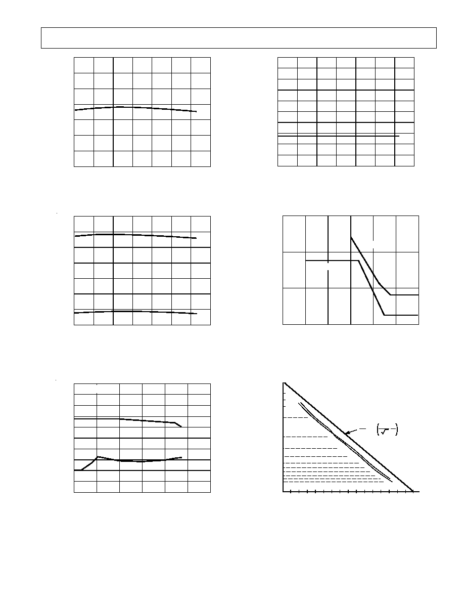
Figure 3. AD800-45 Center Frequency vs. Temperature
52
38
100
44
40
20
42
40
50
46
48
80
60
40
20
0
TEMPERATURE
°
C
DATA RATE Mbps
Figure 5. AD800-45 Capture and Tracking Range vs.
Temperature
55
35
0.30
41
37
0.05
39
0
47
43
45
49
51
53
0.25
0.20
0.15
0.10
INPUT JITTER UI p-p
DATA RATE Mbps
C
D
= 0.68
µ
F
Figure 7. AD800-45 Acquisition Range vs. Input Jitter
10
0
100
3
1
20
2
40
6
4
5
7
8
9
80
60
40
20
0
TEMPERATURE
°
C
JITTER Degrees rms
Figure 4. AD800-45 Jitter vs. Temperature
100
0.1
10
0
10
6
10
1
10
1
10
5
10
4
10
3
10
2
JITTER FREQUENCY Hz
UNIT INTERVALS p-p
AD800-45
DS-3 MASK
Figure 6. AD800-45 Jitter Tolerance
1E-5
1E-11
1E-2
10
12
16
18
22
24
1E-3
1E-4
1E-9
1E-7
1E-1
5E-2
3E-2
2E-2
S/N dB
1
2
erfc
S
N
1
2 2
14
20
80
20
ECL
20
80
BIT ERROR RATE
Figure 8. AD800-45 Bit Error Rate vs. Input Jitter
Typical Characteristics
AD800/AD802
REV. B
6
58
40
100
44
42
20
40
46
48
50
52
54
56
80
60
40
20
0
TEMPERATURE
°
C
CENTER FREQUENCY MHz
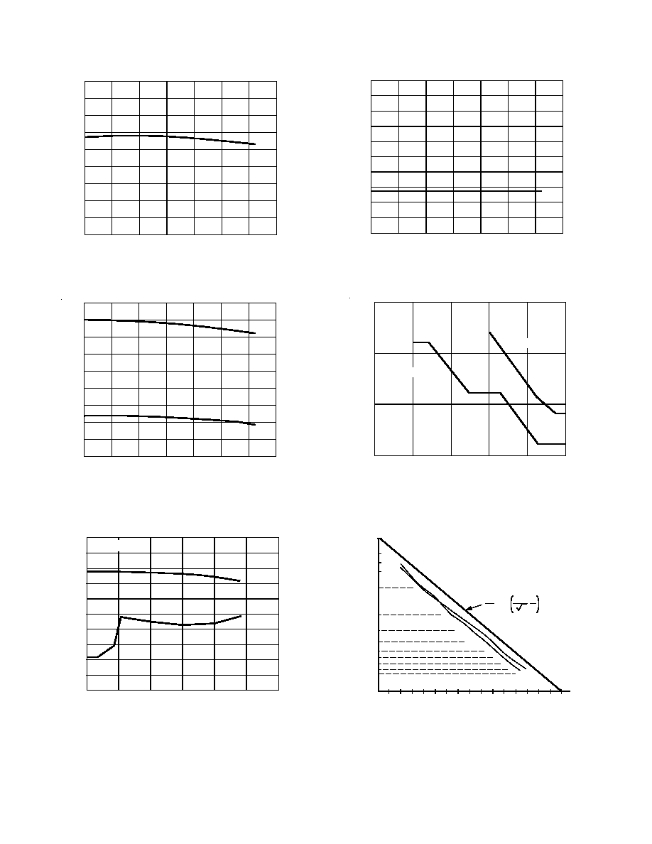
Figure 9. AD800-52 Center Frequency vs. Temperature
58
40
100
44
42
20
40
46
48
50
52
54
56
80
60
40
20
0
TEMPERATURE
°
C
DATA RATE Mbps
Figure 11. AD800-52 Capture and Tracking Range vs.
Temperature
60
40
0.30
46
42
0.05
44
0
52
48
50
54
56
58
0.25
0.20
0.15
0.10
INPUT JITTER UI p-p
DATA RATE Mbps
C
D
= 0.68
µ
F
Figure 13. AD800-52 Acquisition Range vs. Input Jitter
10
0
100
3
1
20
2
40
6
4
5
7
8
9
80
60
40
20
0
TEMPERATURE
°
C
JITTER Degrees rms
Figure 10. AD800-52 Jitter vs. Temperature
100
0.1
10
0
10
1
10
1
10
5
10
4
10
3
10
2
JITTER FREQUENCY Hz
UNIT INTERVALS p-p
AD800-52
OC-1 MASK
Figure 12. AD800-52 Jitter Tolerance
1E-5
1E-10
1E-2
10
12
16
18
22
24
1E-3
1E-4
1E-8
1E-6
1E-1
5E-2
3E-2
2E-2
S/N dB
1
2
erfc
S
N
1
2 2
14
20
80
20
ECL
20
80
BIT ERROR RATE
Figure 14. AD800-52 Bit Error Rate vs. Input Jitter
AD800/AD802
REV. B
7
180
100
120
110
40
140
130
150
160
170
100
80
60
40
20
0
20
TEMPERATURE
°
C
CENTER FREQUENCY MHz
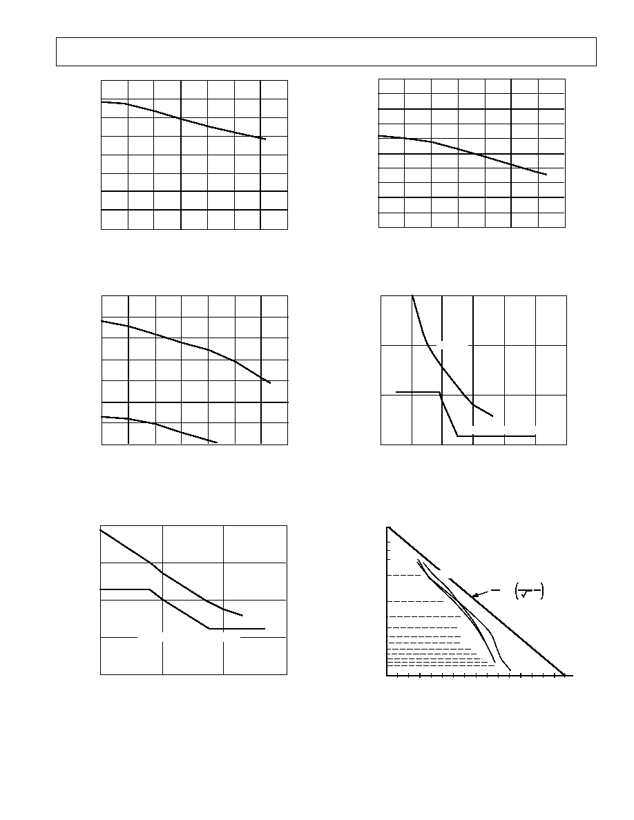
Figure 15. AD802-155 Center Frequency vs. Temperature
TEMPERATURE
°
C
200
130
100
160
140
20
150
40
190
170
180
80
60
40
20
0
DATA RATE Mbps
Figure 17. AD802-155 Capture Range, Tracking Range vs.
Temperature
INPUT JITTER UI
100
0
1
1000
10
0.1
10
1
100
AD802 155
CCITT G.958 STM1 TYPE A MASK
JITTER FREQUENCY Hz
Figure 19. AD802-155 Minimum Acquisition Range vs.
Jitter Frequency, T
MIN
to T
MAX
V
MIN
to V
MAX
100
20
40
10
0
3
1
2
6
4
5
7
8
9
80
60
40
20
0
JITTER Degrees rms
TEMPERATURE
°
C
Figure 16. AD802-155 Output Jitter vs. Temperature
100
0.1
10
2
10
1
UI Pk-Pk
10
3
10
4
10
5
10
8
10
7
10
6
JITTER FREQUENCY Hz
AD802-155
CCITT G.958 STM1 TYPE A MASK
Figure 18. AD802-155 Jitter Tolerance
1E-5
1E-10
1E-2
10
12
16
18
22
24
1E-3
1E-4
1E-8
1E-6
1E-1
5E-2
3E-2
2E-2
BIT ERROR RATE
S/N dB
1
2
erfc
S
N
1
2 2
14
20
80mV
20mV
ECL
20mV
80mV
&
ECL
1E-12
Figure 20. AD802-155 Bit Error Rate vs. Input Jitter
AD800/AD802
REV. B
8
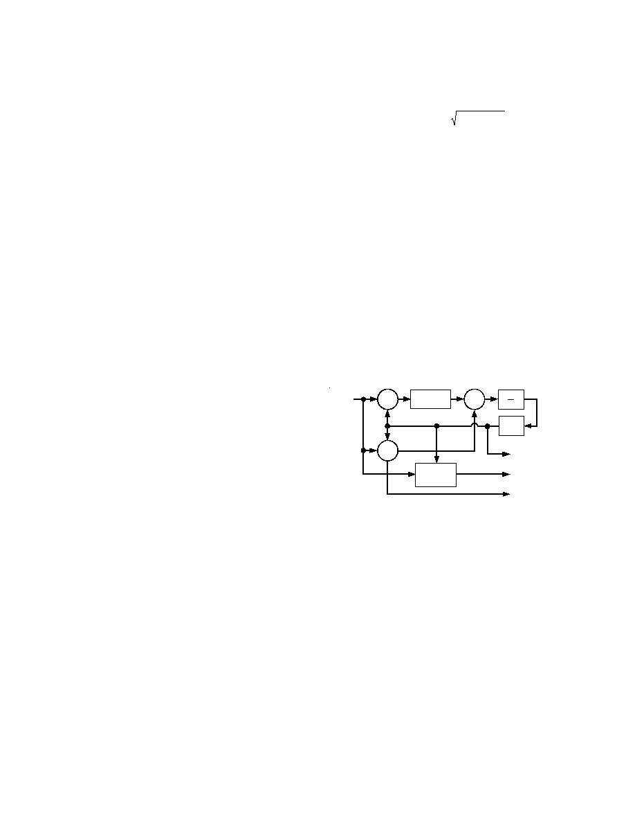
THEORY OF OPERATION
The AD800 and AD802 are phase-locked loop circuits for re-
covery of clock from NRZ data. The architecture uses a fre-
quency detector to aid initial frequency acquisition, refer to
Figure 21 for a block diagram. Note the frequency detector is al-
ways in the circuit. When the PLL is locked, the frequency error
is zero and the frequency detector has no further effect. Since
the frequency detector is always in circuit, no control functions
are needed to initiate acquisition or change mode after acquisi-
tion. The frequency detector also supplies a frequency acquisi-
tion (FRAC) output to indicate when the loop is acquiring lock.
During the frequency acquisition process the FRAC output is a
series of pulses of width equal to the period of the VCO. These
pulses occur on the cycle slips between the data frequency and
the VCO frequency. With a maximum density (1010 . . .) data
pattern, every cycle slip will produce a pulse at FRAC. How-
ever, with random data, not every cycle slip produces a pulse.
The density of pulses at FRAC increases with the density of
data transitions. The probability that a cycle slip will produce a
pulse increases as the frequency error approaches zero. After the
frequency error has been reduced to zero, the FRAC output will
have no further pulses. At this point the PLL begins the process
of phase acquisition, with a settling time of roughly 2000 bit pe-
riods. Valid retimed data can be guaranteed by waiting 2000 bit
periods after the last FRAC pulse has occurred.
Jitter caused by variations of density of data transitions (pattern
jitter) is virtually eliminated by use of a new phase detector
(patented). Briefly, the measurement of zero phase error does
not cause the VCO phase to increase to above the average run
rate set by the data frequency. The jitter created by a 2
7
1
pseudo-random code is 1/2 degree, and this is small compared
to random jitter.
The jitter bandwidth for the AD802-155 is 0.08% of the center
frequency. This figure is chosen so that sinusoidal input jitter at
130 kHz will be attenuated by 3 dB. The jitter bandwidths of
the AD800-45 and AD800-52 are 0.1% of the respective center
frequencies. The jitter bandwidth of the AD800 or the AD802 is
mask programmable from 0.01% to 1% of the center frequency.
A device with a very low loop bandwidth (0.01% of the center
frequency) could effectively filter (clean up) a jittery timing
reference. Consult the factory if your application requires a
special loop bandwidth.
The damping ratio of the phase-locked loop is user program-
mable with a single external capacitor. At 155 MHz a damping
ratio of 10 is obtained with a 0.22
µ
F capacitor. More generally,
the damping ratio scales as
1.7
×
f
DATA
×
C
D
. At 155 MHz a
damping ratio of 1 is obtained with a 2.2 nF capacitor. A lower
damping ratio allows a faster frequency acquisition; generally
the acquisition time scales directly with the capacitor value.
However, at damping ratios approaching one, the acquisition
time no longer scales directly with the capacitor value. The
acquisition time has two components: frequency acquisition and
phase acquisition. The frequency acquisition always scales with
capacitance, but the phase acquisition is set by the loop
bandwidth of the PLL and is independent of the damping ratio.
Thus, the 0.08% fractional loop bandwidth sets a minimum
acquisition time of 15,000 bit periods. Note the acquisition time
for a damping factor of 1 is specified as 15,000 bit periods. This
comprises 13,000 bit periods for frequency acquisition and
2,000 periods for phase acquisition. Compare this to the
400,000 bit periods acquisition time specified for a damping
ratio of 5; this consists entirely of frequency acquisition, and the
2,000 bit periods of phase acquisition is negligible.
While lower damping ratio affords faster acquisition, it also
allows more peaking in the jitter transfer response (jitter
peaking). For example, with a damping ratio of 10 the jitter
peaking is 0.02 dB, but with a damping factor of 1, the peaking
is 2 dB.
DET
Ø
TS + 1
RETIMING
DEVICE
VCO
f
DET
DATA
INPUT
RECOVERED
CLOCK OUTPUT
RETIMED
DATA OUTPUT
FRAC OUTPUT
1
S
Figure 21. AD800 and AD802 Block Diagram
AD800/AD802
REV. B
9
1
2
3
4
5
6
7
8
9
10
20
19
18
17
16
15
14
13
12
11
DATAOUT
DATAOUT
V
CC2
CLKOUT
CLKOUT
AV
EE
ASUBST
FRAC
FRAC
SUBST
DATAIN
DATAIN
AV
CC
CF
1
CF
2
DATAOUT
DATAOUT
CLKOUT
CLKOUT
Z1
AD800/802
J1
J2
R1
R2
R5 100
R10
R6 100
5.0V
R9
R12
R11
R7 100
R8 100
R3
R4
J3
J4
C10
0.1
100
100
154
154
154
154
100
100
C
D
R22
80.6
R21
80.6
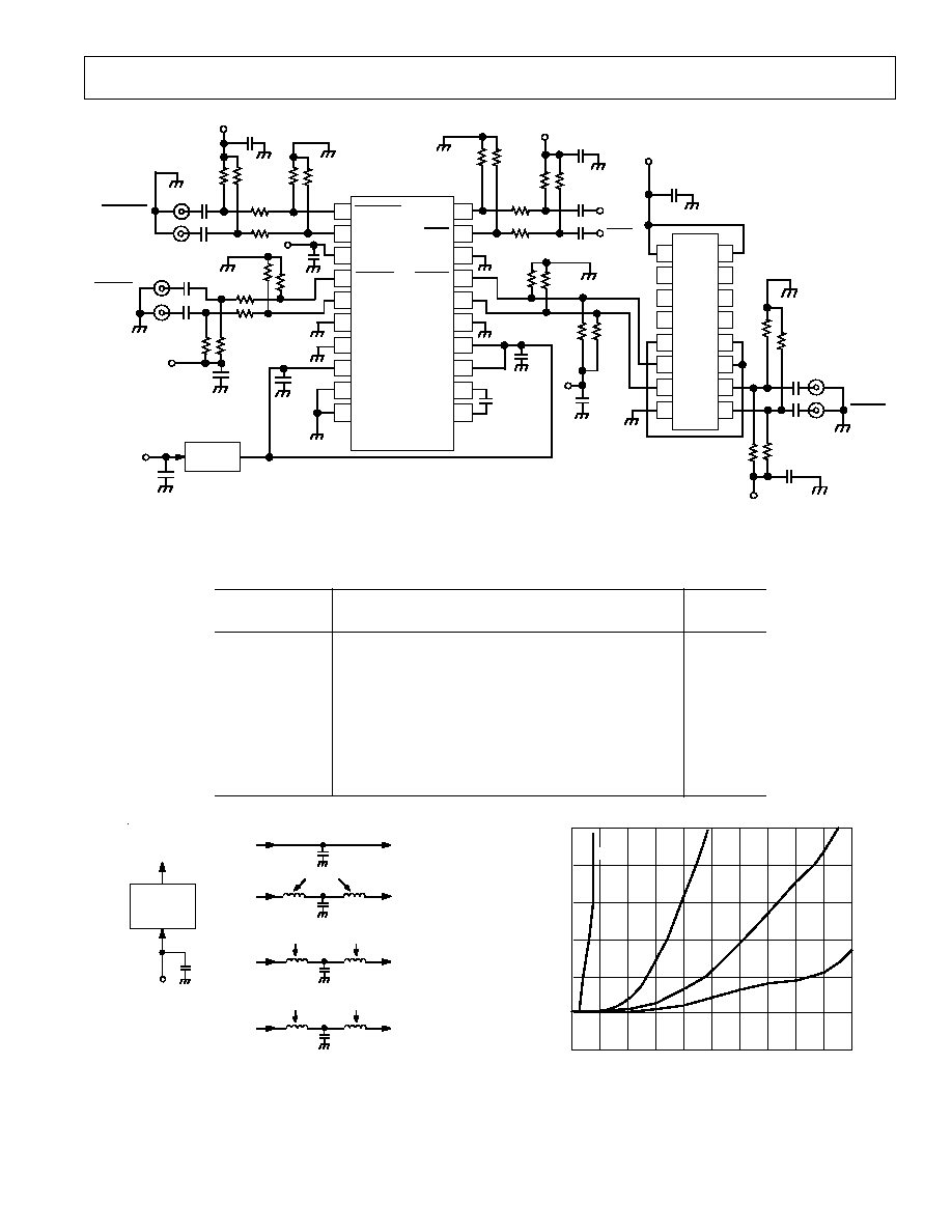
R19
130
R20
130
FRAC
FRAC
5.0V
1
2
3
4
5
6
7
8
16
15
14
13
12
11
10
9
Z2
10H116
R24
130
R23
130
J5
J6
R26
80.6
R25
80.6
DATAIN
DATAIN
5.0V
0.1
0.1
0.1
C7 0.1
C6 0.1
0.1
C16
5.0V
5.0V
R16 100
5.0V
C13 0.1
100
100
154
154
0.1
C20
C21 0.1
5.0V
5.0V
C8
C9
0.1
C5
C4
C3
R13
R14
R15 100
R17
R18
C17 0.1
C14 0.1
C15 0.1
0.1
0.1
C12
C11
C19
0.1
V
EE
C2
10
µ
F
5.0V
BYPASS
NETWORK
OUT
IN
V
EE
V
CC1
V
EE
V
CC1
Figure 22. Evaluation Board Schematic, Positive Supply
Table I. Evaluation Board, Positive Supply: Components List
Reference
Designator
Description
Quantity
R18, R1518
Resistor, 100
, 1%
12
R914
Resistor, 154
, 1%
6
R19, 20, 23, 24
Resistor, 130
, 1%
4
R21, 22, 25, 26
Resistor, 80.6
, 1%
4
C
D
Capacitor, Loop Damping (See Specifications Page)
1
C2
Capacitor, 10
µ
F, Tantalum
1
C3C21
Capacitor, 0.1
µ
F, Ceramic Chip
17
Z1
AD800/AD802
1
Z2
10H116, ECL Line Receiver
1
IN
0.1
µ
F
C2
10
µ
F
BYPASS
NETWORK
(A, B, C,
OR D)
TO DEVICE
IN
5.0V
BEADS WITH ONE LOOP
IN
0.1
µ
F
TO
DEVICE
TO
DEVICE
(A)
IN
0.1
µ
F
TO
DEVICE
BEAD WITH
ONE LOOP
(B)
(C)
BEAD WITH
TWO LOOPS
IN
0.1
µ
F
TO
DEVICE
BEAD WITH
TWO LOOPS
(D)
BEAD WITH
TWO LOOPS
BYPASS NETWORK
COMPONENTS:
CAPACITOR ..........CERAMIC CHIP
FERRITE BEAD......1/4 IN. STACKPOLE CARBO 57-1392
3.0
0
1.0
1.5
0.5
0.1
1.0
0
2.5
2.0
0.9
0.7
0.6
0.5
0.8
0.4
0.3
0.2
JITTER ns p-p
NOISE V p-p @ 311MHz
(A)
(B)
(C)
(D)
Figure 23. Bypass Network Schemes
Figure 24. AD802-155 Output Jitter vs. Supply Noise
(PECL Configuration)
AD800/AD802
REV. B
10
BYPASS
NETWORK
(A, B, C,
OR D)
MICRO
METALS
T50-10
TO
DEVICE
PINS
6, 7, 9
10, 15,
18
PINS
8, 13,
14
AD802-155
PIN
3
IN
0.47
µ
F
0.47
µ
F
10 TURNS
10
µ
F
5V
50
NOISE IN
SENSE
Figure 25. Power Supply Noise Sensitivity Test Circuit, PECL Configuration
1
2
3
4
5
6
7
8
9
10
20
19
18
17
16
15
14
13
12
11
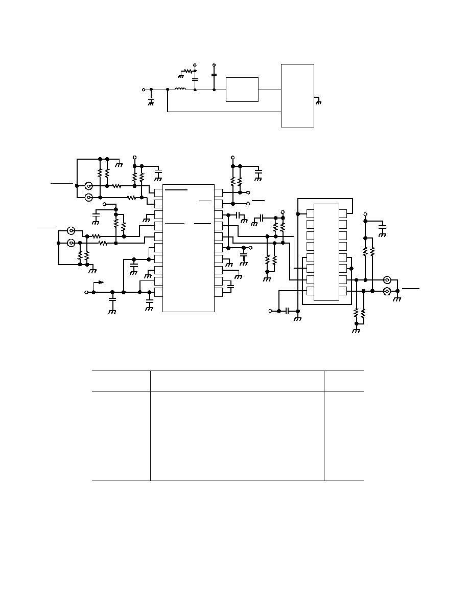
5.2V
DATAOUT
CLKOUT
V
EE
AV
EE
ASUBST
FRAC
SUBST
DATAIN
V
CC1
AV
CC
CF
1
CF
2
DATAOUT
CLKOUT
FRAC
DATAIN
DATAOUT
CLKOUT
DATAOUT
CLKOUT
1
2
3
4
5
6
7
8
Z2
10H116
Z1
AD800/802
J1
J2
R1
R2
R5 100
R10
C3
R6 100
5.2V
R9
C4
R12
R11
R7 100
R8 100
R3
R4
J3
J4
5.2V
C5
100
100
154
154
0.1
0.1
154
154
100
100
0.1
C2
10
C6
0.1
C10
0.1
5.2V
C
D
R14
80.6
R13
80.6
C7
0.1
5.2V
0.1
R21
274
R22
274
C8 0.1
C9 0.1
R15
130
R16
130
FRAC
5.2V
16
15
14
13
12
11
10
9
C11
0.1
R20
130
R19
130
J5
J6
R18
80.6
R17
80.6
DATAIN
DATAIN
5.2V
5.2V
--5.2V
C12
V
CC2
V
EE
V
EE
V
CC1
FRAC
Figure 26. Evaluation Board Schematic, Negative Supply
Table II. Evaluation Board, Negative Supply: Components List
Reference
Designator
Description
Quantity
R18
Resistor, 100
, 1%
8
R912
Resistor, 154
, 1%
4
R13, 14, 17, 18
Resistor, 80.6
, 1%
4
R15, 16, 19, 20
Resistor, 130
, 1%
4
R21, 22
Resistor, 274
, 1%
2
C
D
Capacitor, Loop Damping (See Specifications Page)
1
C2
Capacitor, 10
µ
F, Tantalum
1
C3C12
Capacitor, 0.1
µ
F, Ceramic Chip
10
Z1
AD800/AD802
1
Z2
10H116, ECL Line Receiver
1
AD800/AD802
REV. B
11
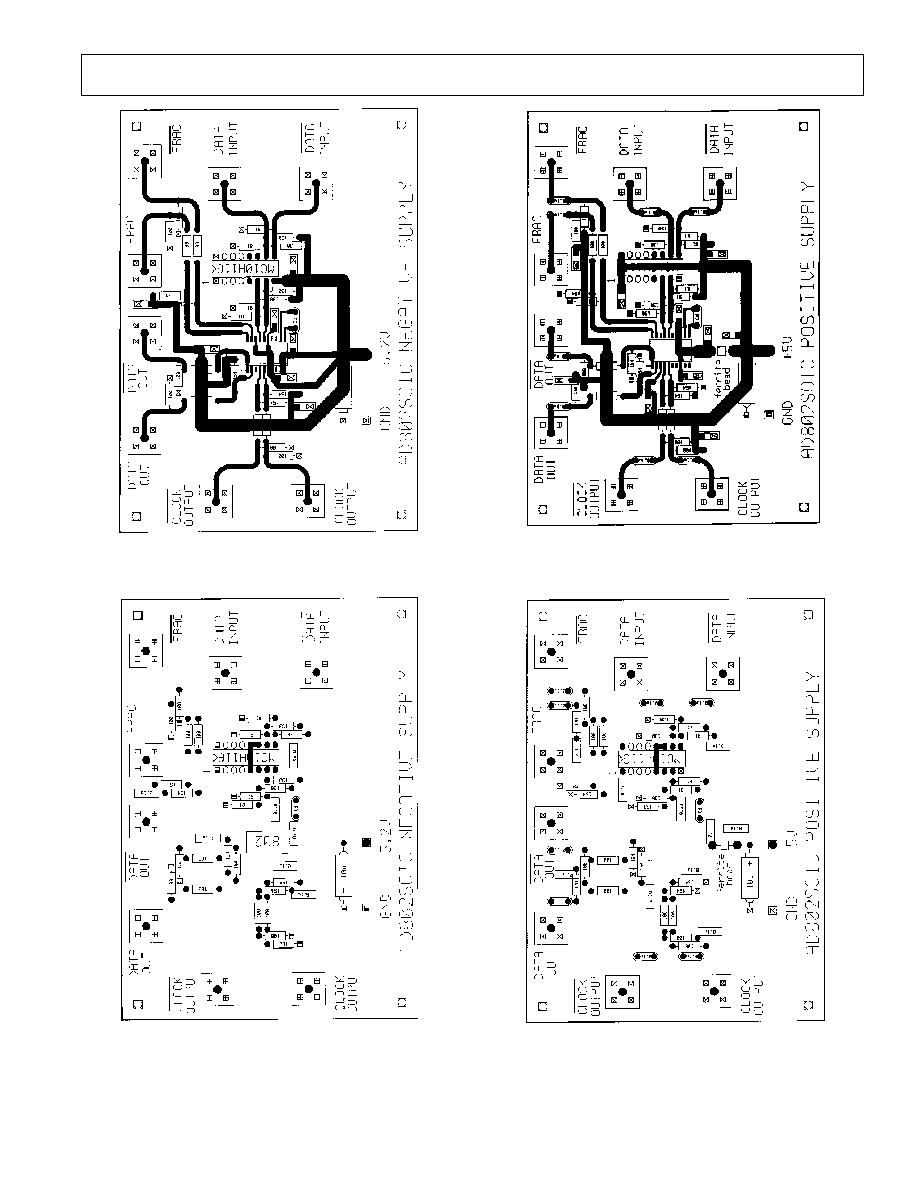
Figure 27. Negative Supply Configuration: Component
Side (Top Layer)
Figure 28. Negative Supply Configuration: Solder Side
Figure 29. Positive Supply Configuration: Component
Side (Top Layer)
Figure 30. Positive Supply Configuration: Solder Side
AD800/AD802
REV. B
12
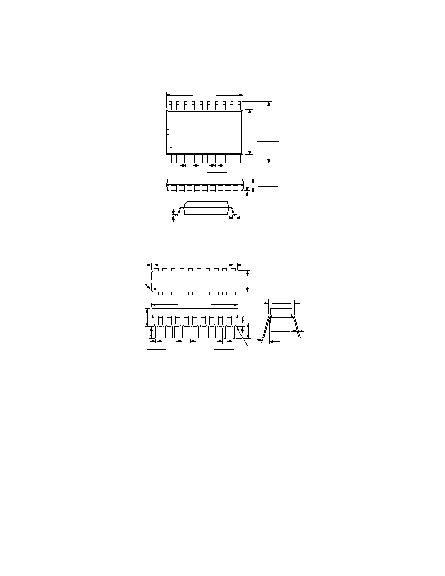
OUTLINE DIMENSIONS
Dimensions shown in inches and (mm).
20-Pin Small Outline IC Package (R-20)
1
10
11
20
0.50 (1.27)
BSC
0.015 (0.38)
0.007 (0.18)
0.019 (0.48)
0.014 (0.36)
0.011 (0.28)
0.004 (0.10)
0.050 (1.27)
0.016 (0.40)
0.104 (2.64)
0.093 (2.36)
0.419 (10.65)
0.394 (10.00)
0.300 (7.60)
0.292 (7.40)
0.512 (13.00)
0.496 (12.60)
20-Pin Cerdip Package (Q-20)
0.320 (8.13)
0.290 (7.37)
0.015 (0.38)
0.008 (0.20)
15
°
0
°
0.005 (0.13) MIN
PIN 1
0.098 (2.49) MAX
0.310 (7.87)
0.220 (5.59)
10
11
1
20
1.060 (26.92) MAX
0.200
(5.08)
MAX
0.023 (0.58)
0.014 (0.36)
0.200 (5.08)
0.125 (3.18)
0.100
(2.54)
BSC
0.070 (1.78)
0.030 (0.76)
0.060 (1.52)
0.015 (0.38)
0.150
(3.81)
MIN
SEATING
PLANE
C1725a7.512/93
PRINTED IN U.S.A.