REV. C
Information furnished by Analog Devices is believed to be accurate and
reliable. However, no responsibility is assumed by Analog Devices for its
use, nor for any infringements of patents or other rights of third parties
which may result from its use. No license is granted by implication or
otherwise under any patent or patent rights of Analog Devices.
a
LC
2
MOS
16-Bit, High Speed Sampling ADCs
AD7884/AD7885
© Analog Devices, Inc., 1995
One Technology Way, P.O. Box 9106, Norwood, MA 02062-9106, U.S.A.
Tel: 617/329-4700
Fax: 617/326-8703
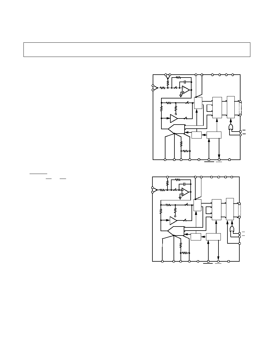
FUNCTIONAL BLOCK DIAGRAMS
±
5V F
±
5V S
±
3V F
±
3V S
16-BIT
ACCURATE
DAC
AD7884
TIMER
CONTROL
DGND
CS
RD
BUSY
DB15
V S
REF+
REF+
V F
V
REF
AGNDS
AGNDF AV
DD
V
SS
GND
DB0
V
INV
CONVST
IN
V
DD
AV
SS
R7
2k
R8
2k
9
9
9
16
16
V
REF
5k
3k
3k
4k
4k
R1
R2
R3
R4
C1
SW1
R5
SW2
SW3
2k
R6
A1
A2
9-BIT
ADC
LATCH
+
ALU
O
U
T
P
U
T
D
R
I
V
E
R
S
IN
IN
IN
±
5V F
±
5V S
16-BIT
ACCURATE
DAC
AD7885
TIMER
CONTROL
DGND
CS
RD
BUSY
DB7
V S
REF+
V F
REF+
V
REF
AGNDS
AGNDF AV
DD
V
SS
GND
DB0
V
INV
CONVST
IN
V
DD
AV
SS
R7
2k
R8
2k
9
9
9
16
8
V
REF
5k
3k
2k
4k
4k
R1
R2
3k
R3
R4
C1
SW1
R5
SW2
SW3
R6
A1
A2
9-BIT
ADC
LATCH
+
ALU
O
U
T
P
U
T
D
R
I
V
E
R
S
IN
IN
±
3V
HBEN
FEATURES
Monolithic Construction
Fast Conversion: 5.3 s
High Throughput: 166 kSPS
Low Power: 250 mW
APPLICATIONS
Automatic Test Equipment
Medical Instrumentation
Industrial Control
Data Acquisition Systems
Robotics
GENERAL DESCRIPTION
The AD7884/AD7885 is a 16-bit monolithic analog-to-digital
converter with internal sample-and-hold and a conversion time
of 5.3
µ
s. The maximum throughput rate is 166 kSPS. It uses a
two pass flash architecture to achieve this speed. Two input
ranges are available:
±
5 V and
±
3 V. Conversion is initiated by
the CONVST signal. The result can be read into a microproces-
sor using the CS and RD inputs on the device. The AD7884 has
a 16-bit parallel reading structure while the AD7885 has a byte
reading structure. The conversion result is in 2s complement
code.
The AD7884/AD7885 has its own internal oscillator which con-
trols conversion. It runs from
±
5 V supplies and needs a V
REF+
of +3 V.
The AD7884 is available in a 40-pin plastic DIP package and in
a 44-pin PLCC package.
The AD7885 is available in a 28-pin plastic DIP package and
the AD7885A is available in a 44-pin PLCC package.

REV. C
2
AD7884/AD7885/AD7885ASPECIFICATIONS
(V
DD
= +5 V 5%, V
SS
= 5 V 5%, V
REF
+S
= +3 V; AGND = DGND = GND = 0 V; f
SAMPLE
= 166 kHz. All specifications T
MIN
to T
MAX
, unless otherwise noted.)
A
B
Parameter
Version
1, 2, 3
Versions
1, 2, 3
Units
Test Conditions/Comments
DC ACCURACY
Resolution
16
16
Bits
Minimum Resolution for Which
No Missing Codes Are Guaranteed
16
16
Bits
Integral Nonlinearity
±
0.0075
% FSR max
Typically 0.003% FSR
Positive Gain Error
±
0.03
±
0.03
% FSR typ
AD7885AN/BN: 0.1% typ
Positive Gain Error
±
0.05
% FSR max
AD7885BN: 0.2% max
Gain TC
4
±
2
±
2
ppm FSR/
°
C typ
Bipolar Zero Error
±
0.05
±
0.05
% FSR typ
Bipolar Zero Error
±
0.15
% FSR max
Bipolar Zero TC
4
±
8
±
8
ppm FSR/
°
C typ
Negative Gain Error
±
0.03
±
0.03
% FSR typ
AD7885AN/BN: 0.1% typ
Negative Gain Error
±
0.05
% FSR max
AD7885BN: 0.2% max
Offset TC
4
±
2
±
2
ppm FSR/
°
C typ
Noise
120
120
µ
V rms typ
78
µ
V rms typical in
±
3 V Input Range
DYNAMIC PERFORMANCE
Signal to (Noise + Distortion) Ratio
84
84
dB min
Input Signal:
±
5 V, 1 kHz Sine Wave, Typically 86 dB
82
82
dB typ
Input Signal:
±
5 V, 12 kHz Sine Wave
Total Harmonic Distortion
88
88
dB max
Input Signal:
±
5 V, 1 kHz Sine Wave
84
84
dB typ
Input Signal:
±
5 V, 12 kHz Sine Wave
Peak Harmonic or Spurious Noise
88
88
dB max
Input Signal:
±
5 V, 1 kHz Sine Wave
Intermodulation Distortion (IMD)
2nd Order Terms
84
84
dB typ
f
A
= 11.5 kHz, f
B
= 12 kHz, f
SAMPLE
= 166 kHz
3rd Order Terms
84
84
dB typ
f
A
= 11.5 kHz, f
B
= 12 kHz, f
SAMPLE
= 166 kHz
CONVERSION TIME
Conversion Time
5.3
5.3
µ
s max
Acquisition Time
2.5
2.5
µ
s max
Throughput Rate
166
166
kSPS max
There is an overlap between conversion and acquisition.
ANALOG INPUT
Voltage Range
±
5
±
5
Volts
±
3
±
3
Volts
Input Current
±
4
±
4
mA max
REFERENCE INPUT
Reference Input Current
±
5
±
5
mA max
V
REF
+ S = +3 V
LOGIC INPUTS
Input High Voltage, V
INH
2.4
2.4
V min
V
DD
= 5 V
±
5%
Input Low Voltage, V
INL
0.8
0.8
V max
V
DD
= 5 V
±
5%
Input Current, I
IN
±
10
±
10
µ
A max
Input Level = 0 V to V
DD
Input Capacitance, C
IN
4
10
10
pF max
LOGIC OUTPUTS
Output High Voltage, V
OH
4.0
4.0
V min
I
SOURCE
= 40
µ
A
Output Low Voltage, V
OL
0.4
0.4
V max
I
SINK
= 1.6 mA
DB15DB0
Floating-State Leakage Current
10
10
µ
A max
Floating-State Output Capacitance
4
15
15
pF max
POWER REQUIREMENTS
V
DD
+5
+5
V nom
±
5% for Specified Performance
V
SS
5
5
V nom
±
5% for Specified Performance
I
DD
35
35
mA max
Typically 25 mA
I
SS
30
30
mA max
Typically 25 mA
Power Supply Rejection Ratio
Gain/
V
DD
86
86
dB typ
Gain/
V
SS
86
86
dB typ
Power Dissipation
325
325
mW max
Typically 250 mW
NOTES
1
Temperature ranges are as follows: A, B Versions: 40
°
C to +85
°
C.
2
V
IN
=
±
5 V.
3
The AD7885AAP has the same specs as the AD7884AP. The AD7885ABP has the same specs as the AD7884BP.
4
Sample tested to ensure compliance.
Specifications subject to change without notice.

AD7884/AD7885
REV. C
3
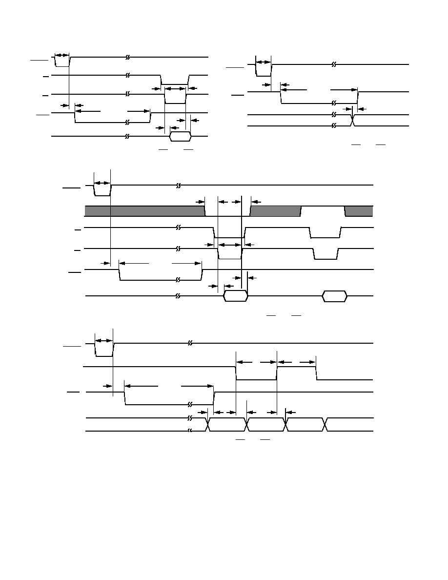
TIMING CHARACTERISTICS
1, 2
Limit at +25 C
Limit at T
MIN
, T
MAX
Parameter
(All Versions)
(A, B Versions)
Units
Conditions/Comments
t
1
50
50
ns min
CONVST
Pulse Width
t
2
100
100
ns max
CONVST
to BUSY Low Delay
t
3
0
0
ns min
CS
to RD Setup Time
t
4
60
60
ns min
RD
Pulse Width
t
5
0
0
ns min
CS
to RD Hold Time
t
6
2
57
57
ns max
Data Access Time after RD
t
7
3
5
5
ns min
Bus Relinquish Time after RD
50
50
ns max
t
8
40
40
ns min
New Data Valid before Rising Edge of BUSY
t
9
10
80
ns min
HBEN to RD Setup Time
t
10
25
25
ns min
HBEN to RD Hold Time
t
11
60
60
ns min
HBEN Low Pulse Duration
t
12
60
60
ns min
HBEN High Pulse Duration
t
13
55
70
ns max
Propagation Delay from HBEN Falling to Data Valid
t
14
55
70
ns max
Propagation Delay from HBEN Rising to Data Valid
NOTES
1
Timing specifications in bold print are 100% production tested. All other times are sample tested at +5
°
C to ensure compliance. All input signals are specified
with tr = tf = 5 ns (10% to 90% of 5 V) and timed from a voltage level of 1.6 V.
2
t
6
is measured with the load circuit of Figure 1 and defined as the time required for an output to cross 0.8 V or 2.4 V.
3
t
7
is derived from the measured time taken by the data outputs to change 0.5 V when loaded with the circuit of Figure 1. The measured number is then extrap-
olated back to remove the effects of charging or discharging the 100 pF capacitor. This means that the time, t
7
, quoted in the Timing Characteristics is the true
bus relinquish time of the part and as such is independent of external bus loading capacitances.
Specifications subject to change without notice.
(V
DD
= +5 V 5%, V
SS
= 5 V 5%, AGND = DGND = GND = 0 V. See Figures 2, 3, 4 and 5.)
ORDERING GUIDE
Linearity
Temperature
Error
SNR
Package
Model
1
Range
(% FSR)
(dB)
Option
2
AD7884AN
40
°
C to +85
°
C
84
N-40A
AD7884BN
40
°
C to +85
°
C
±
0.0075
84
N-40A
AD7884AP
40
°
C to +85
°
C
84
P-44A
AD7884BP
40
°
C to +85
°
C
±
0.0075
84
P-44A
AD7885AN
40
°
C to +85
°
C
84
N-28A
AD7885BN
40
°
C to +85
°
C
±
0.0075
84
N-28A
AD7885AAP 40
°
C to +85
°
C
84
P-44A
AD7885ABP 40
°
C to +85
°
C
±
0.0075
84
P-44A
NOTES
1
Analog Devices reserves the right to ship cerdip (Q) packages in lieu of plastic
DIP (N) packages.
2
N = Plastic DIP; P = Plastic Leaded Chip Carrier (PLCC).
TO OUTPUT PIN
+2.1V
I
OH
I
OL
C
L
100pF
1.6mA
200
µ
A
Figure 1. Load Circuit for Access Time and Bus Relinquish
Time
AD7884/AD7885
REV. C
4
CS
RD
DATA
BUSY
CONVST
t
1
t
3
t
6
t
4
CONVERT
t
Hi-Z
t
2
DATA
VALID
t
5
t
7
Hi-Z
Figure 2. AD7884 Timing Diagram, Using CS and RD
DATA
OLD DATA VALID
NEW DATA VALID
BUSY
CONVST
t
1
t
2
t
8
t
CONVERT
Figure 3. AD7884 Timing Diagram, with CS and RD
Permanently Low
HBEN
CS
RD
DATA
BUSY
CONVST
Hi-Z
Hi-Z
DB0DB7
DB8DB15
Hi-Z
t
1
t
3
t
6
t
4
t
5
t
7
t
2
CONVERT
t
DATA
VALID
t
9
t
10
DATA
VALID
Figure 4. AD7885 Timing Diagram, Using CS and RD
DATA
BUSY
OLD DATA VALID
(DB8 DB15)
NEW DATA VALID
(DB8 DB15)
NEW DATA VALID
(DB0 DB7)
NEW DATA VALID
(DB8 DB15)
NEW DATA VALID
(DB0 DB7)
HBEN
CONVST
t
1
t
2
CONVERT
t
t
8
t
13
t
14
t
11
t
12
Figure 5. AD7885 Timing Diagram, with CS and RD Permanently Low

AD7884/AD7885
REV. C
5
ABSOLUTE MAXIMUM RATINGS
1
V
DD
to AGND . . . . . . . . . . . . . . . . . . . . . . . . . 0.3 V to +7 V
AV
DD
to AGND . . . . . . . . . . . . . . . . . . . . . . . . 0.3 V to +7 V
V
SS
to AGND . . . . . . . . . . . . . . . . . . . . . . . . . +0.3 V to 7 V
AV
SS
to AGND . . . . . . . . . . . . . . . . . . . . . . . . 0.3 V to 7 V
AGND Pins to DGND . . . . . . . . . . . . 0.3 V to V
DD
+ 0.3 V
AV
DD
to V
DD
2
. . . . . . . . . . . . . . . . . . . . . . . . . 0.3 V to +7 V
AV
SS
to V
SS
2
. . . . . . . . . . . . . . . . . . . . . . . . . . +0.3 V to 7 V
GND to DGND . . . . . . . . . . . . . . . . . 0.3 V to V
DD
+ 0.3 V
V
IN
S, V
IN
F to AGND . . . . . . . . . . V
SS
0.3 V to V
DD
+ 0.3 V
V
REF+
to AGND . . . . . . . . . . . . . . . V
SS
0.3 V to V
DD
+ 0.3 V
V
REF
to AGND . . . . . . . . . . . . . . . V
SS
0.3 V to V
DD
+ 0.3 V
V
INV
to AGND . . . . . . . . . . . . . . . V
SS
0.3 V to V
DD
+ 0.3 V
Digital Inputs to DGND . . . . . . . . . . . 0.3 V to V
DD
+ 0.3 V
Digital Outputs to DGND . . . . . . . . . . 0.3 V to V
DD
+ 0.3 V
Operating Temperature Range
Commercial Plastic (A, B Versions) . . . . . 40
°
C to +85
°
C
Industrial Cerdip (A, B Versions) . . . . . . . . 40
°
C to +85
°
C
Extended Cerdip (T Versions) . . . . . . . . 55
°
C to +125
°
C
Storage Temperature Range . . . . . . . . . . . 65
°
C to +150
°
C
Lead Temperature (Soldering, 10 secs) . . . . . . . . . . . +300
°
C
Power Dissipation (Any Package) to +75
°
C . . . . . . . 1000 mW
Derates above +75
°
C by . . . . . . . . . . . . . . . . . . . . 10 mW/
°
C
1
Stresses above those listed under "Absolute Maximum Ratings" may cause
permanent damage to the device. This is a stress rating only and functional
operation of the device at these or any other conditions above those listed in the
operational sections of this specification is not implied. Exposure to absolute
maximum rating conditions for extended periods may affect device reliability.
2
If the AD7884/AD7885 is being powered from separate analog and digital supplies,
AV
SS
should always come up before V
SS
. See Figure 12 for a recommended
protection circuit using Schottky diodes.
WARNING!
ESD SENSITIVE DEVICE
CAUTION
ESD (electrostatic discharge) sensitive device. Electrostatic charges as high as 4000 V readily
accumulate on the human body and test equipment and can discharge without detection.
Although these devices feature proprietary ESD protection circuitry, permanent damage may
occur on devices subjected to high energy electrostatic discharges. Therefore, proper ESD
precautions are recommended to avoid performance degradation or loss of functionality.
PIN CONFIGURATIONS
DIP
DB2
DB1
DB0
DB13
DGND
DB11
AV
SS
V
DD
DB7
DB6
DB5
DB4
DB3
CS
RD
BUSY
DB8
DB9
DB10
DB12
V
DD
DB15
DB14
V
INV
V S
REF+
V F
REF+
V
REF
AGNDS
AGNDF
AV
DD
V
SS
GND
V
SS
±
3V S
IN
V
SS
CONVST
GND
1
2
3
4
5
6
7
8
9
10
40
39
38
37
36
35
34
33
32
31
TOP VIEW
(Not to Scale)
AD7884
30
29
28
27
26
25
24
23
22
21
11
12
13
14
15
16
17
18
19
20
IN
±
3V F
±
5V S
IN
IN
±
5V F
1
2
3
7
28
27
26
22
8
9
10
21
20
19
11
12
18
17
4
5
25
24
6
23
TOP VIEW
(Not to Scale)
13
14
16
15
AD7885
AV
SS
V
DD
CS
RD
V
INV
V
REF
AGNDS
AGNDF
AV
DD
GND
±
3V
IN
V
SS
CONVST
±
5V S
IN
IN
±
5V F
DB2
DB1
DB0
DGND
DB7
DB6
DB5
DB4
DB3
V S
REF+
V F
REF+
BUSY
HBEN
PLCC
±5V
IN
F
±3V
IN
F
AD7884
TOP VIEW
(Not to Scale)
2
1
44
3
4
5
6
42
41
40
43
18
19
20
21
22
23
24
25
26
27
28
39
38
37
36
35
34
33
32
31
30
29
7
8
9
10
11
12
13
14
15
16
17
DGND
DB11
AV
DD
DB7
DB6
DB5
DB2
DB1
DB0
DB4
DB3
DB8
DB9
DB10
DB12
DB13
DB15
DB14
V
REF+
S
V
REF+
F
AGNDS
AGNDF
AV
SS
V
SS
GND
CS
RD
BUSY
CONVST
GND
V
INV
V
REF
±3V
IN
S
±5V
IN
S
NC
NC
NC
NC
NC = NO CONNECT
V
SS
V
DD
V
SS
V
DD
AD7885A
TOP VIEW
(Not to Scale)
2
1
44
3
4
5
6
42
41 40
43
18
19
20
21
22
23
24
25
26
27
28
39
38
37
36
35
34
33
32
31
30
29
7
8
9
10
11
12
13
14
15
16
17
DGND
DB6
DB3
DB2
DB1
DB0
DB4
DB5
NC
DB7
V
DD
NC
NC
NC
AGNDS
AGNDF
GND
CS
RD
BUSY
HBEN
CONVST
GND
NC
NC
NC
NC
NC = NO CONNECT
NC
NC
NC
NC
±5V
IN
F
AV
DD
AV
SS
V
SS
V
SS
V
DD
±3V
IN
F
V
REF+
S
V
REF+
F
V
INV
V
REF
±3V
IN
S
±5V
IN
S
AD7884/AD7885
REV. C
6
PIN FUNCTION DESCRIPTION
AD7884
AD7885
AD7885A
Description
V
INV
V
INV
V
INV
This pin is connected to the inverting terminal of an op amp, as in Figure 6, and allows
the inversion of the supplied +3 V reference.
V
REF
V
REF
V
REF
This is the negative reference input, and it can be obtained by using an external amplifier
to invert the positive reference input. In this case, the amplifier output is connected to
V
REF.
See Figure 6.
±
3 V
IN
S
_
±
3 V
IN
S
This is the analog input sense pin for the
±
3 volt analog input range on the AD7884 and
AD7885A.
±
3 V
IN
F
_
±
3 V
IN
F
This is the analog input force pin for the
±
3 volt analog input range on the AD7884 and
AD7885A. When using this input range, the
±
5 V
IN
F and
±
5 V
IN
S pins should be tied to
AGND.
±
3 V
IN
This is the analog input pin for the
±
3 volt analog input range on the AD7885. When us-
ing this input range, the
±
5 V
IN
F and
±
5 V
IN
S pins should be tied to AGND.
±
5 V
IN
S
±
5 V
IN
S
±
5 V
IN
S
This is the analog input sense pin for the
±
5 volt analog input range on both the AD7884,
AD7885 and AD7885A.
±
5 V
IN
F
±
5 V
IN
F
±
5 V
IN
F
This is the analog input force pin for the
±
5 volt analog input range on both the AD7884,
AD7885 and AD7885A. When using this input range, the
±
3 V
IN
F and
±
3 V
IN
S pins
should be tied to AGND.
AGNDS
AGNDS
AGNDS
This is the ground return sense pin for the 9-bit ADC and the on-chip residue amplifier.
AGNDF
AGNDF
AGNDF
This is the ground return force pin for the 9-bit ADC and the on-chip residue amplifier.
AV
DD
AV
DD
AV
DD
Positive analog power rail for the sample-and-hold amplifier and the residue amplifier.
AV
SS
AV
SS
AV
SS
Negative analog power rail for the sample-and-hold amplifier and the residue amplifier.
GND
GND
GND
This is the ground return for sample-and-hold section.
V
SS
V
SS
V
SS
Negative supply for the 9-bit ADC.
V
DD
V
DD
V
DD
Positive supply for the 9-bit ADC and all device logic.
CONVST
CONVST
CONVST
This asynchronous control input starts conversion.
CS
CS
CS
Chip Select control input.
RD
RD
RD
Read control input. This is used in conjunction with CS to read the conversion result
from the device output latch.
HBEN
HBEN
High Byte Enable. Active high control input for the AD7885. It selects either the high or
the low byte of the conversion for reading.
BUSY
BUSY
BUSY
Busy output. The Busy output goes low when conversion begins and stays low until it is
completed, at which time it goes high.
DB0DB15
Sixteen-bit parallel data word output on the AD7884.
DB0DB7
DB0DB7
Eight-bit parallel data byte output on the AD7885.
DGND
DGND
DGND
Ground return for all device logic.
V
REF+
F
V
REF+
F
V
REF+
F
Reference force input.
V
REF+
S
V
REF+
S
V
REF+
S
Reference sense input. The device operates from a +3 V reference.
AD7884/AD7885
REV. C
7
TERMINOLOGY
Integral Nonlinearity
This is the maximum deviation from a straight line passing
through the endpoints of the ADC transfer function.
Differential Nonlinearity
This is the difference between the measured and the ideal 1 LSB
change between any two adjacent codes in the ADC.
Bipolar Zero Error
This is the deviation of the midscale transition (all 0s to all 1s)
from the ideal (AGND).
Positive Gain Error
This is the deviation of the last code transition (01 . . . 110 to
01 . . . 111) from the ideal (+V
REF+
S 1 LSB), after Bipolar
Zero Error has been adjusted out.
Negative Gain Error
This is the deviation of the first code transition (10 . . . 000 to
10 . . . 001) from the ideal (V
REF+
S + 1 LSB), after Bipolar
Zero Error has been adjusted out.
Signal to (Noise + Distortion) Ratio
This is the measured ratio of signal to (noise + distortion) at the
output of the A/D converter. The signal is the rms amplitude of
the fundamental. Noise is the rms sum of all nonfundamental
signals up to half the sampling frequency (f
S
/2), excluding dc.
The ratio is dependent upon the number of quantization levels
in the digitization process; the more levels, the smaller the quan-
tization noise. The theoretical signal to (noise + distortion) ratio
for an ideal N-bit converter with a sine wave input is given by:
Signal to (Noise + Distortion) = (6.02N + 1.76) dB
Thus for an ideal 16-bit converter, this is 98 dB.
Total Harmonic Distortion
Total harmonic distortion (THD) is the ratio of the rms sum of
harmonics to the fundamental. For the AD7884/AD7885, it is
defined as:
THD (dB)
=
20 log
V
2
2
+
V
3
2
+
V
4
2
+
V
5
2
+
V
6
2
V
1
where V
1
is the rms amplitude of the fundamental and V
2
, V
3
,
V
4
, V
5
and V
6
are the rms amplitudes of the second through the
sixth harmonics.
Peak Harmonic or Spurious Noise
Peak harmonic or spurious noise is defined as the ratio of the
rms value of the next largest component in the ADC output
spectrum (up to f
S
/2 and excluding dc) to the rms value of the
fundamental. Normally, the value of this specification is deter-
mined by the largest harmonic in the spectrum, but for parts
where the harmonics are buried in the noise floor, it will be a
noise peak.
Intermodulation Distortion
With inputs consisting of sine waves at two frequencies, fa and
fb, any active device with nonlinearities will create distortion
products at sum and difference frequencies of mfa
±
nfb where
m, n = 0, 1, 2, 3, etc. Intermodulation terms are those for which
neither m or n are equal to zero. For example, the second order
terms include (fa + fb) and (fa fb), while the third order terms
include (2fa + fb), (2fa fb), (fa + 2fb) and (fa 2fb).
The AD7884/AD7885 is tested using the CCIFF standard
where two input frequencies near the top end of the input band-
width are used. In this case, the second and third order terms
are of different significance. The second order terms are usually
distanced in frequency from the original sine waves while the
third order terms are usually at a frequency close to the input
frequencies. As a result, the second and third order terms are
specified separately. The calculation of the intermodulation dis-
tortion is as per the THD specification where it is the ratio of
the rms sum of the individual distortion products to the rms am-
plitude of the fundamental expressed in dBs.
Power Supply Rejection Ratio
This is the ratio, in dBs, of the change in positive gain error to
the change in V
DD
or V
SS
. It is a dc measurement.
OPERATIONAL DIAGRAM
An operational diagram for the AD7884/AD7885 is shown in
Figure 6. It is set up for an analog input range of
±
5 V. If a
±
3 V input range is required, A1 should drive
±
3 V
IN
S and
±
3 V
IN
F with
±
5 V
IN
S,
±
5 V
IN
F being tied to system AGND.
±3V
IN
F
±5V
IN
F
5V
+5V
AD817
AD711
AD817
AGNDS
AGNDF
AD7884
AD7885
A1
A3
A4
AD845, AD817 OR
EQUIVALENT
NOTE: POWER SUPPLY DECOUPLING NOT SHOWN
A2
GND
DGND
V
DD
= +5V
DATA
OUTPUTS
CONTROL
INPUTS
V
INV
V
REF+
S
V
REF+
F
V
REF
±3V
IN
S
±5V
IN
S
AV
SS
V
DD
AV
DD
V
SS
V
IN
AD845, AD817 OR
EQUIVALENT
AD780
2
6
8
4
10µF
Figure 6. AD7884/AD7885 Operational Diagram
The chosen input buffer amplifier (A1) should have low noise
and distortion and fast settling time for high bandwidth applica-
tions. Both the AD711 and the AD845 are suitable amplifiers.
A2 is the force, sense amplifier for AGND. The AGNDS pin
should be at zero potential. Therefore, the amplifier must have a
low input offset voltage and good noise performance. It must
also have the ability to deal with fast current transients on the
AGNDS pin. The AD817 has the required performance and is
the recommended amplifier.
If AGNDS and AGNDF are simply tied together to Star
Ground instead of buffering, the SNR and THD are not signifi-
cantly degraded. However, dc specifications like INL, Bipolar
Zero and Gain Error will be degraded.

AD7884/AD7885
REV. C
8
The required +3 V reference is derived from the AD780 and
buffered by the high-speed amplifier A3 (AD845, AD817 or
equivalent). A4 is a unity gain inverter which provides the 3 V
negative reference. The gain setting resistors are on-chip and
are factory trimmed to ensure precise tracking of V
REF+
. Figure
6 shows A3 and A4 as AD845s or AD817s. These have the ability
to respond to the rapidly changing reference input impedance.
CIRCUIT DESCRIPTION
Analog Input Section
The analog input section of the AD7884/AD7885 is shown in
Figure 7. It contains both the input signal conditioning and
sample-and-hold amplifier. Note that the analog input is truly
benign. When SW1a goes open circuit to put the SHA into the
hold mode, SW1b is closed. This means that the input resis-
tors, R1 and R2 are always connected to either virtual ground
or true ground.
IN
±
5V F
R2 5k
R1 3k
R3 3k
C1
SW1a
A1
IN
±
5V S
IN
±
3V F
IN
±
3V S
R4 4k
R6 2k
R5 4k
TO RESIDUE
AMPLIFIER A2
TO
9-BIT
ADC
V
REF
SW1b
Figure 7. AD7884/AD7885 Analog Input Section
When the
±
3 V
IN
S and
±
3 V
IN
F inputs are tied to 0 V, the in-
put section has a gain of 0.6 and transforms an input signal
of
±
5 volts to the required
±
3 volts. When the
±
5 V
IN
S and
±
5 V
IN
F inputs are grounded, the input section has a gain of
1 and so the analog input range is now
±
3 volts. Resistors R4
and R5, at the amplifier output, further condition the
±
3 volts
signal to be 0 to 3 volts. This is the required input for the 9-bit
A/D converter section.
With SW1a closed, the output of A1 follows the input (the
sample-and-hold is in the track mode). On the rising edge of
the CONVST pulse, SW1a goes open circuit, and capacitor C1
holds the voltage on the output of A1. The sample-and-
hold is now in the hold mode. The aperture delay time for the
sample-and-hold is nominally 50 ns.
A/D Converter Section
The AD7884/AD7885 uses a two-pass flash technique in order
to achieve the required speed and resolution. When the CONVST
control input goes from low to high, the sample-and-hold ampli-
fier goes into the hold mode and a 0 V to 3 V signal is pre-
sented to the input of the 9-bit ADC. The first phase of
conversion generates the 9 MSBs of the 16-bit result and trans-
fers these to the latch and ALU combination. They are also fed
back to the 9 MSBs of the 16-bit DAC. The 7 LSBs of the
DAC are permanently loaded with 0s. The DAC output is sub-
tracted from the analog input with the result being amplified
and offset in the Residue Amplifier Section. The signal at the
output of A2 is proportional to the error between the first phase
result and the actual analog input signal and is digitized in the
second conversion phase. This second phase begins when the
16-bit DAC and the Residue Error Amplifier have both settled.
First, SW2 is turned off and SW3 is turned on. Then, the SHA
section of the Residue Amplifier goes into hold mode. Next
SW2 is turned off and SW3 is turned on. The 9-bit result is
transferred to the output latch and ALU. An error correction al-
gorithm now compensates for the offset inserted in the Residue
Amplifier Section and errors introduced in the first pass conver-
sion and combines both results to give the 16-bit answer.
9
9
V
REF
2k
4k
4k
R4
R5
SW2
SW3
R6
A2
9-BIT
ADC
LATCH
+
ALU
16
0 TO 3V
±
3V SIGNAL
FROM INPUT
SHA
16-BIT
ACCURATE
DAC
V S
REF+
REF+
V F
V
REF
V
INV
R7
2k
R8
2k
9
+3V
3V
RESIDUE AMP
+
SHA
Figure 8. A/D Converter Section
AD7884/AD7885
REV. C
9
Timing and Control Section
Figure 9 shows the timing and control sequence for the
AD7884/AD7885. When the part receives a CONVST pulse,
the conversion begins. The input sample-and-hold goes into the
hold mode 50 ns after the rising edge of CONVST and BUSY
goes low. This is the first phase of conversion and takes 3.35
µ
s
to complete. The second phase of conversion begins when SW2
is turned off and SW3 turned on. The Residue Amplifier and
SHA section (A2 in Figure 8) goes into hold mode at this point
and allows the input sample-and-hold to go back into sample
mode. Thus, while the second phase of conversion is ongoing,
the input sample-and-hold is also acquiring the input signal for
the next conversion. This overlap between conversion and ac-
quisition allows throughput rates of 166 kSPS to be achieved.
CONVST
BUSY
SAMPLE
HOLD
INPUT
SHA
FIRST PHASE
3.5
µ
s
TACQ
2.5
µ
s
SECOND
PHASE
FIRST PHASE OF CONVERSION
1ST 9-BIT CONVERSION
DAC SETTLING TIME
RESIDUE AMPLIFIER
SETTLING TIME
SECOND PHASE OF CONVERSION
2ND 9-BIT CONVERSION
ERROR CORRECTION
OUTPUT LATCH UPDATE
1.8
µ
s
Figure 9. Timing and Control Sequence
USING THE AD7884/AD7885 ANALOG INPUT RANGES
The AD7884/AD7885 can be set up to have either a
±
3 volts
analog input range or a
±
5 volts analog input range. Figures 10
and 11 show the necessary corrections for each of these. The
output code is 2s complement and the ideal code table for both
input ranges is shown in Table I.
Reference Considerations
The AD7884/AD7885 operates from a
±
3 volt reference. This
can be derived simply using the AD780 as shown in Figure 6.
A1
V
INV
±
3V S
IN
IN
±
3V F
±
5V S
IN
IN
±
5V F
Figure 10.
±
5 V Input Range Connection
±
3V S
IN
IN
±
3V F
±
5V S
IN
IN
±
5V F
A1
V
INV
Figure 11.
±
3 V Input Range Connections
The critical performance specification for a reference in a 16-bit
application is noise. The reference pk-pk noise should be insig-
nificant in comparison to the ADC noise. The AD7884/
AD7885 has a typical rms noise of 120
µ
V. For example a rea-
sonable target would be to keep the total rms noise less than
125
µ
V. To do this the reference noise needs to be less than
35
µ
V rms. In the 100 kHz band, the AD780 noise is less than
30
µ
V rms, making it a very suitable reference.
The buffer amplifier used to drive the device V
REF+
should have
low enough noise performance so as not to affect the overall
system noise requirement. The AD845 and AD817 achieve
this.
Table I. Ideal Output Code Table for the AD7884/AD7885
Analog Input
Digital Output
In Terms of FSR
2
3 V Range
3
5 V Range
4
Code Transition
l
+FSR/2 1 LSB
2.999908
4.999847
011 . . . 111 to 111 . . . 110
+FSR/2 2 LSBs
2.999817
4.999695
011 . . . 110 to 011 . . . 101
+FSR/2 3 LSBs
2.999726
4.999543
011 . . . 101 to 011 . . . 100
AGND + 1 LSB
0.000092
0.000153
000 . . . 001 to 000 . . . 000
AGND
0.000000
0.000000
000 . . . 000 to 111 . . . 111
AGND 1 LSB
0.000092
0.000153
111 . . . 111 to 111 . . . 110
(FSR/2 3 LSBs)
2.999726
4.999543
100 . . . 011 to 100 . . . 010
(FSR/2 2 LSBs)
2.999817
4.999695
100 . . . 010 to 100 . . . 001
(FSR/2 1 LSB)
2.999908
4.999847
100 . . . 001 to 100 . . . 000
NOTES
1
This table applies for V
REF+
S = +3 V.
2
FSR (Full-Scale Range) is 6 volts for the
±
3 V input range and 10 volts for the
±
5 V input range.
3
1 LSB on the
±
3 V range is FSR/2
16
and is equal to 91.5
µ
V.
4
1 LSB on the
±
5 V range is FSR/2
16
and is equal to 152.6
µ
V.

AD7884/AD7885
REV. C
10
Decoupling and Grounding
The AD7884 and AD7885A have one AV
DD
pin and two V
DD
pins. They also have one AV
SS
pin and three V
SS
pins. The
AD7885 has one AV
DD
pin, one V
DD
pin, one AV
SS
pin and one
V
SS
pin. Figure 6 shows how a common +5 V supply should be
used for the positive supply pins and a common 5 V supply for
the negative supply pins.
For decoupling purposes, the critical pins on both devices are
the AV
DD
and AV
SS
pins. Each of these should be decoupled to
system AGND with 10
µ
F tantalum and 0.1
µ
F ceramic capaci-
tors right at the pins. With the V
DD
and V
SS
pins, it is sufficient
to decouple each of these with ceramic 1
µ
F capacitors.
AGNDS, AGNDF are the ground return points for the on-chip
9-bit ADC. They should be driven by a buffer amplifier as
shown in Figure 6. If they are tied directly together and then
to ground, there will he a marginal degradation in linearity
performance.
The GND pin is the analog ground return for the on-chip linear
circuitry. It should he connected to system analog ground.
The DGND pin is the ground return for the on-chip digital
circuitry. It should be connected to the ground terminal of the
V
DD
and V
SS
supplies. If a common analog supply is used for
AV
DD
and V
DD
then DGND should be connected to the com-
mon ground point.
Power Supply Sequencing
AV
DD
and V
DD
are connected to a common substrate and there
is typically 17
resistance between them. If they are powered
by separate +5 V supplies, then these should come up simulta-
neously. Otherwise, the one that comes up first will have to
drive +5 V into a 17
load for a short period of time. However,
the standard short-circuit protection on regulators like the 7800
series will ensure that there is no possibility of damage to the
driving device.
AV
SS
should always come up either before or at the same time
as V
SS
. If this cannot be guaranteed, Schottky diodes should be
used to ensure that V
SS
never exceeds AV
SS
by more than 0.3 V.
Arranging the power supplies as in Figure 6 and using the recom-
mended decoupling ensures that there are no power supply
sequencing issues as well as giving the specified noise performance.
AV
DD
V
DD
AV
SS
V
SS
+5V
+5V
5V
5V
AD7884/AD7885
HP5082-2810
OR
EQUIVALENT
Figure 12. Schottky Diodes Used to Protect Against
Incorrect Power Supply Sequencing
AD7884/AD7885 PERFORMANCE
Linearity
The linearity of the AD7884/AD7885 is determined by the
on-chip 16-bit D/A converter. This is a segmented DAC which
is laser trimmed for 16-bit DNL performance to ensure that
there are no missing codes in the ADC transfer function. Figure
13 shows a typical INL plot for the AD7884/AD7885.
0
16384
32768
49152
65535
0
0.5
1.0
1.5
2.0
OUTPUT CODE
LINEARITY ERROR LSBs
V = +5V
V = 5V
T = +25
°
C
DD
SS
A
Figure 13. AD7884/AD7885 Typical Linearity Performance
Noise
In an A/D converter, noise exhibits itself as code uncertainty in
dc applications and as the noise floor (in an FFT, for example)
in ac applications.
In a sampling A/D converter like the AD7884/AD7885, all in-
formation about the analog input appears in the baseband from
dc to 1/2 the sampling frequency. An antialiasing filter will re-
move unwanted signals above f
S
/2 in the input signal but the
converter wideband noise will alias into the baseband. In the
AD7884/AD7885, this noise is made up of sample-and-hold
noise and A/D converter noise. The sample-and-hold section
contributes 51
µ
V rms and the ADC section contributes 59
µ
V
rms. These add up to a total rms noise of 78
µ
V. This is the in-
put referred noise in the
±
3 V analog input range. When operat-
ing in the
±
5 V input range, the input gain is reduced to 0.6.
This means that the input referred noise is now increased by a
factor of 1.66 to 120
µ
V rms.
Figure 14 shows a histogram plot for 5000 conversions of a dc
input using the AD7884/AD7885 in the
±
5 V input range. The
analog input was set as close as possible to the center of a code
transition. All codes other than the center code are due to the
ADC noise. In this case, the spread is six codes.
3000
0
2000
1000
CODE FREQUENCY
(X 2) (X 1)
(X)
(X + 1) (X + 2) (X + 3)
CODE
Figure 14. Histogram of 5000 Conversions of a DC Input

AD7884/AD7885
REV. C
11
If the noise in the converter is too high for an application, it can
be reduced by oversampling and digital filtering. This involves
sampling the input at higher than the required word rate and
then averaging to arrive at the final result. The very fast conver-
sion time of the AD7884/AD7885 makes it very suitable for
oversampling. For example, if the required input bandwidth is
40 kHz, the AD7884/AD7885 could be oversampled by a factor
of 2. This yields a 3 dB improvement in the effective SNR per-
formance. The noise performance in the
±
5 volt input range is
now effectively 85
µ
V rms and the resultant spread of codes for
2500 conversions will be four. This is shown in Figure 15.
1500
0
1000
500
CODE FREQUENCY
(X 1)
(X)
(X + 1) (X + 2)
CODE
Figure 15. Histogram of 2500 Conversions of a DC Input
Using a
×
2 Oversampling Ratio
Dynamic Performance
With a combined conversion and acquisition time of 6
µ
s, the
AD7884/AD7885 is ideal for wide bandwidth signal processing
applications. Signal to (Noise + Distortion), Total Harmonic
Distortion, Peak Harmonic or Spurious Noise and Intermodula-
tion Distortion are all specified. Figure 16 shows a typical
FFT plot of a 1.8 kHz,
±
5 V input after being digitized by the
AD7884/AD7885.
0
150
60
120
90
30
2048 POINT FFT
dB
f = 1.8kHz,
±
5V SINE WAVE
f = 163kHz
SNR = 87dB
THD = 95dB
IN
SAMPLE
Figure 16. AD7884/AD7885 FFT Plot
Effective Number of Bits
The formula for SNR (see Terminology section) is related to
the resolution or number of bits in the converter. Rewriting the
formula, below, gives a measure of performance expressed in
effective number of bits (N).
N = (SNR 1.76)/6.02
16
10
80
13
11
20
12
0
15
14
60
40
FREQUENCY kHz
EFFECTIVE NUMBER OF BITS
Figure 17. Effective Number of Bits vs. Frequency
The effective number of bits for a device can be calculated from
its measured SNR. Figure 17 shows a typical plot of effective
number of bits versus frequency for the AD7884. The sampling
frequency is 166 kHz.
MICROPROCESSOR INTERFACING
The AD7884/AD7885 is designed on a high speed process
which results in very fast interfacing timing (Data Access Time
of 57 ns max). The AD7884 has a full 16-bit parallel bus, and
the AD7885 has an 8-bit wide bus. The AD7884, with its paral-
lel interface, is suited to 16-bit parallel machines whereas the
AD7885, with its byte interface, is suited to 8-bit machines.
Some examples of typical interface configurations follow.
AD7884 to MC68000 Interface
Figure 18 shows a general interface diagram for the MC68000,
16-bit microprocessor to the AD7884. In Figure 18, conversion
is initiated by bringing CSA low (i.e., writing to the appropriate
address). This allows the processor to maintain control over the
complete conversion process. In some cases it may be more
desirable to control conversion independent from the processor.
This can be done by using an external sampling timer.
MC68000
AD7884
ADDRESS
DECODE LOGIC
CONVST
CS
RD
DB15 DB0
R/W
DATA BUS
ADDRESS BUS
A23 A1
D15 D0
DTACK
AS
CSA
CSB
Figure 18. AD7884 to MC68000 Interface
Once conversion has been started, the processor must wait until
it is completed before reading the result. There are two ways of
ensuring this. The first way is to simply use a software delay to
wait for 6.5
µ
s before bringing CS and RD low to read the data.
AD7884/AD7885
REV. C
12
The second way is to use the BUSY output of the AD7884 to
generate an interrupt in the MC68000. Because of the nature of
its interrupts, the MC68000 requires additional logic (not
shown in Figure 18) to allow it to be interrupted correctly. For
full information on this, consult the MC68000 User's Manual.
AD7884 to 80286 Interface
The 80286 is an advanced high performance processor with spe-
cial capabilities aimed at multiuser and multitasking systems.
Figure 19 shows an interface configuration for the AD7884 to
such a system. Note that only signals relevant to the AD7884
are shown. For the full 80286 configuration refer to the iAPX
286 data sheet (Basic System Configuration).
In Figure 19 conversion is started by writing to a selected ad-
dress and causing it CS2 to go low. When conversion is com-
plete, BUSY goes high and initiates an interrupt. The processor
can then read the conversion result.
82288 BUS
CONTROLLER
MRDC
CLK
82284 CLOCK
GENERATOR
CLK
8282 OR
8283
LATCH
8286 OR 8287
TRANSCEIVER
DECODE
CIRCUITRY
CS1
CS2
8259A
INTERRUPT
CONTROLLER
CLK
80286
CPU
D D
15
0
A A
23
0
AD7884
RD
CS
CONVST
DB15
DB0
BUSY
IR IR
0
7
MEMORY READ
Figure 19. AD7884 Interfacing to Basic iAPX 286 System

AD7884/AD7885
REV. C
13
AD7885 to 8088 Interface
The AD7885, with its byte (8 + 8) data format, is ideal for use
with the 8088 microprocessor. Figure 20 is the interface dia-
gram. Conversion is started by enabling CSA. At the end of
conversion, data is read into the processor. The read instruc-
tions are:
MOV AX, C001
Read 8 MSBs of data
MOV AX, C000
Read 8 LSBs of data
8088
AD7885
ADDRESS
DECODE LOGIC
A15 A8
AD7 AD0
MN/MX
+5 V
HBEN
IO/M
ALE
A0
RD
ADDRESS BUS
CONVST
CS
RD
DB7 DB0
CSA
CSB
DATA BUS
STB
8282
Figure 20. AD7885 to 8088 Interface
AD7884 to ADSP-2101 Interface
Figure 21 shows an intcrface between the AD7884 and the
ADSP-2101. Conversion is initiated using a timer which allows
very accurate control of the sampling instant. The AD7884
BUSY
line provides an interrupt to the ADSP-2101 when con-
version is completed. The RD pulse width of the processor can
be programmed using the Data Memory Wait State Control
Register. The result can then be read from the ADC using the
following instruction:
MR0 = DM (ADC)
where MR0 is the ADSP-2101 MR0 register, and
where
ADC is the AD7884 address.
ADDRESS
DECODE LOGIC
ADSP-2101
DMA13 DMA0
DMD15 DMD0
IRQn
DMS
RD
EN
TIMER
AD7884
ADDRESS BUS
DATA BUS
CONVST
CS
RD
DB15 DB0
BUSY
Figure 21. AD7884 to ADSP-2101 Interface
Stand-Alone Operation
If CS and RD are tied permanently low on the AD7884, then,
when a conversion is completed, output data will be valid on the
rising edge of BUSY. This makes the device very suitable for
stand-alone operation. All that is required to run the device is an
external CONVST pulse which can be supplied by a sample
timer. Figure 22 shows the AD7884 set up in this mode with the
BUSY
signal providing the clock for the 74HC574 3-state
latches.
TIMER
AD7884
CONVST
CS
RD
DB15 DB8
BUSY
HBEN
A0
74HC574
74HC574
CLK
CLK
DB7 DB0
Figure 22. Stand-Alone Operation
Digital Feedthrough from an Active Bus
It is very important when using the AD7884/AD7885 in a
microprocessor-based system to isolate the ADC data bus from
the active processor bus while a conversion is being executed.
This will yield the best noise performance from the ADC.
Latches like the 74HC574 can be used to do this. If the device
is connected directly to an active bus then the converter noise
will typically increase by a factor of 30%.

AD7884/AD7885
REV. C
14
OUTLINE DIMENSIONS
Dimensions shown in inches and (mm).
28-Pin Plastic DIP (N-28A)
1.450 (36.83)
1.440 (35.576)
0.550 (13.97)
0.530 (13.462)
28
1
14
15
SEATING
PLANE
0.020 (0.508)
0.015 (0.381)
0.105 (2.67)
0.095 (2.41)
0.200
(5.080)
MAX
0.175 (4.45)
0.120 (3.05)
0.06 (1.52)
0.05 (1.27)
15
°
0
°
0.606 (15.39)
0.594 (15.09)
0.012 (0.305)
0.008 (0.203)
0.160 (4.06)
0.140 (3.56)
LEADS ARE SOLDER DIPPED OR TIN-PLATED ALLOY 42 OR COPPER.
40-Pin Plastic DIP (N-40A)
0.55 (13.97)
0.53 (13.46)
0.025 (0.64)
0.015 (0.38)
0.100 (2.54)
BSC
0.200
(5.08)
MAX
0.175 (4.45)
0.120 (3.05)
0.060 (1.52)
0.040 (1.02)
0.060 (1.52)
0.015 (0.38)
0.140
(3.56)
MIN
PLANE
SEATING
PIN 1
20
1
21
40
0.015 (0.38)
0.008 (0.20)
0.620 (15.75)
0.580 (14.73)
0.110 (2.79) MAX
0.005 (0.13) MIN
2.08 (52.83) MAX
0
°
-15
°

AD7884/AD7885
REV. C
15
44-Pin PLCC (P-44A)
0.020 (0.508) MIN
0.021 (0.533)
0.013 (0.331)
PIN 1
IDENTIFIER
TOP VIEW
0.050 ± 0.005
(1.27 ± 0.13)
0.032 (0.812)
0.026 (0.661)
0.695 (17.65)
0.685 (17.40)
SQ
SQ
0.630 (16.00)
0.590 (14.99)
R.020 (0.508) MAX
3 PLCS
0.045 (1.143) TYP
0.045
(1.143)
TYP
0.045 (1.143) TYP
0.045
(1.143)
TYP
0.120 (3.04)
0.090 (2.29)
0.180 (4.57)
0.165 (4.20)
0.656 (16.662)
0.650 (16.510)

C1620b53/95
PRINTED IN U.S.A.
16