Äîêóìåíòàöèÿ è îïèñàíèÿ www.docs.chipfind.ru
REV. 0
Information furnished by Analog Devices is believed to be accurate and
reliable. However, no responsibility is assumed by Analog Devices for its
use, nor for any infringements of patents or other rights of third parties
which may result from its use. No license is granted by implication or
otherwise under any patent or patent rights of Analog Devices.
a
LC
2
MOS, High Speed
1-, 4- & 8-Channel 10-Bit ADCs
AD7776/AD7777/AD7778*
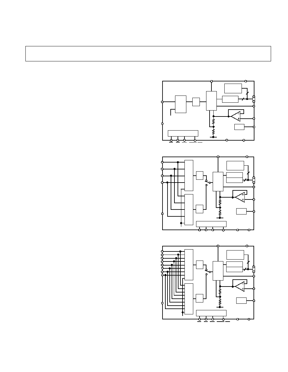
FUNCTIONAL BLOCK DIAGRAMS
CS
RD WR BUSY/INT
AGND
DB0DB9
AD7776
10
DGND
CLKIN
10
CONTROL
REGISTER
ADCREG1
T/H
REFOUT
REFIN
REF
AGND
C
REFIN
RTN
V
SWING
V
BIAS
A
IN
1
MUX
REFIN
10-BIT
ADC
CONTROL LOGIC
V
CC
AGND
DB0DB9
AD7777
10
CONTROL
REGISTER
DGND
CLKIN
10
ADCREG2
ADCREG1
T/H
1
REFOUT
REFIN
REF
AGND
C
REFIN
V
SWING
V
BIAS
A
IN
1
A
IN
2
A
IN
3
A
IN
4
MUX
1
REFIN
T/H
2
MUX
2
10-BIT
ADC
CONTROL LOGIC
V
CC
RTN
AGND
DB0DB9
AD7778
10
CONTROL
REGISTER
DGND
CLKIN
CS
RD WR BUSY/INT
10
ADCREG2
ADCREG1
T/H
1
REFOUT
REFIN
REF
AGND
C
REFIN
V
SWING
V
BIAS
A
IN
1
A
IN
2
A
IN
3
A
IN
4
A
IN
5
A
IN
6
A
IN
7
A
IN
8
MUX
1
REFIN
T/H
2
MUX
2
10-BIT
ADC
CONTROL LOGIC
V
CC
RTN
FEATURES
AD7776: Single Channel
AD7777: 4-Channel
AD7778: 8-Channel
Fast 10-Bit ADC: 2.5 s Worst Case
+5 V Only
Half-Scale Conversion Option
Fast Interface Port
Power-Down Mode
APPLICATIONS
HDD Servos
Instrumentation
GENERAL DESCRIPTION
The AD7776, AD7777 and AD7778 are a family of high speed,
multichannel, 10-bit ADCs primarily intended for use in R/W
head positioning servos found in high density hard disk drives.
They have unique input signal conditioning features that make
them ideal for use in such single supply applications.
By setting a bit in a control register within both the four-channel
version, AD7777, and the eight-channel version, AD7778, the
input channels can either be independently sampled or any two
channels of choice can be simultaneously sampled. For all ver-
sions the specified input signal range is of the form V
BIAS
±
V
SWING
. However, if the RTN pin is biased at, say, 2 V the
analog input signal range becomes 0 V to +2 V for all input
channels. This is covered in more detail under the section
Changing the Analog Input Voltage Range. The voltage V
BIAS
is the offset of the ADC's midpoint code from ground and is
supplied either by an onboard reference available to the user
(REFOUT) or by an external voltage reference applied to
REFIN. The full-scale range (FSR) of the ADC is equal to
2 V
SWING
where V
SWING
is nominally equal to REFIN/2. Addi-
tionally, when placed in the half-scale conversion mode, the
value of REFIN is converted. This allows the channel offset(s)
to be measured.
Control register loading and ADC register reading, channel se-
lect and conversion start are under the control of the
µ
P. The
twos complemented coded ADCs are easily interfaced to a stan-
dard 16-bit MPU bus via their 10-bit data port and standard
microprocessor control lines.
The AD7776/AD7777/AD7778 are fabricated in linear compat-
ible CMOS (LC
2
MOS), an advanced, mixed technology process
that combines precision bipolar circuits with low power CMOS
logic. The AD7776 is available in a 24-pin SOIC package; the
AD7777 is available in both 28-pin DIP and 28-pin SOIC pack-
ages; the AD7778 is available in a 44-pin PQFP package.
*Protected by U.S. Patent No. 4,990,916.
One Technology Way, P.O. Box 9106, Norwood, MA 02062-9106, U.S.A.
Tel: 617/329-4700
World Wide Web Site: http://www.analog.com
Fax: 617/326-8703
© Analog Devices, Inc., 1997

REV. 0
2
AD7776/AD7777/AD7778SPECIFICATIONS
(V
CC
= +5 V 5%; AGND = DGND = O V;
CLKIN = 8 MHz; RTN = O V; C
REFIN
= 10 nF; all specifications T
MIN
to T
MAX
unless otherwise noted.)
Parameter
A Versions
1
Units
Conditions/Comments
DC ACCURACY
Resolution
2
10
Bits
Relative Accuracy
±
1
LSB max
See Terminology
Differential Nonlinearity
±
1
LSB max
No Missing Codes; See Terminology
Bias Offset Error
±
12
LSB max
See Terminology
Bias Offset Error Match
10
LSB max
Between Channels, AD7777/AD7778 Only; See Terminology
Plus or Minus Full-Scale Error
±
12
LSB max
See Terminology
Plus or Minus Full-Scale Error Match 10
LSB max
Between Channels, AD7777/AD7778 Only; See Terminology
ANALOG INPUTS
Input Voltage Range
All Inputs
V
BIAS
±
V
SWING
V min/V max
Input Current
+200
µ
A max
V
IN
= V
BIAS
±
V
SWING
; Any Channel
REFERENCE INPUT
REFIN
1.9/2.1
V min/V max
For Specified Performance
REFIN Input Current
+200
µ
A max
REFERENCE OUTPUT
REFOUT
1.9/2.1
V min/V max
Nominal REFOUT = 2.0 V
DC Output Impedance
5
typ
Reference Load Change
±
2
mV max
For Reference Load Current Change of 0 to
±
500
µ
A
±
5
mV max
For Reference Load Current Change of 0 to
±
1 mA
Reference Load Should Not Change During Conversion
Short Circuit Current
3
20
mA max
See Terminology
LOGIC OUTPUTS
DB0DB9,
BUSY/INT
V
OL
, Output Low Voltage
0.4
V max
I
SINK
= 1.6 mA
V
OH
, Output High Voltage
4.0
V min
I
SOURCE
= 200
µ
A
Floating State Leakage Current
±
10
µ
A max
Floating State Capacitance
3
10
pF max
ADC Output Coding
Twos Complement
LOGIC INPUTS
DB0DB9,
CS, WR, RD, CLKIN
Input Low Voltage, V
INL
0.8
V max
Input High Voltage, V
INH
2.4
V min
Input Leakage Current
10
µ
A max
Input Capacitance
3
10
pF max
CONVERSION TIMING
Acquisition Time
4.5 t
CLKIN
ns min
See Terminology
5.5 t
CLKIN
+ 70
ns max
Single Conversion
14 t
CLKIN
ns max
Double Conversion
28 t
CLKIN
ns max
t
CLKIN
125/500
ns min/ns max Period of Input Clock CLKIN
t
CLKIN
High
50
ns min
Minimum High Time for CLKIN
t
CLKIN
Low
40
ns min
Minimum Low Time for CLKIN
POWER REQUIREMENTS
V
CC
Range
+4.75/+5.25
V min/V max
For Specified Performance
I
CC
, Normal Mode
15
mA max
CS = RD = +5 V, CR8 = 0
I
CC
, Power-Down Mode
1.5
mA max
CR8 = 1. All Linear Circuitry OFF
Power-Up Time to Operational
Specifications
500
µ
s max
From Power-Down Mode
DYNAMIC PERFORMANCE
See Terminology
Signal to Noise and Distortion
S/(N+D) Ratio
57
dB min
V
IN
= 99.88 kHz Full-Scale Sine Wave with f
SAMPLING
= 380.95 kHz
Total Harmonic Distortion (THD)
60
dB min
V
IN
= 99.88 kHz Full-Scale Sine Wave with f
SAMPLING
= 380.95 kHz
Intermodulation Distortion (IMD)
75
dB typ
fa = 103.2 kHz, fb = 96.5 kHz with f
SAMPLING
= 380.95 kHz. Both
Signals Are Sine Waves at Half-Scale Amplitude
Channel-to-Channel Isolation
90
dB typ
V
IN
= 100 kHz Full-Scale Sine Wave with f
SAMPLING
= 380.95 kHz
NOTES
1
Temperature range as follows: A = 40
°
C to +85
°
C.
2
1 LSB = (2
×
V
SWING
)/1024 = 1.95 mV for V
SWING
= 1.0 V.
3
Guaranteed by design, not production tested.
Specifications subject to change without notice.
AD7776/AD7777/AD7778
3
REV. 0
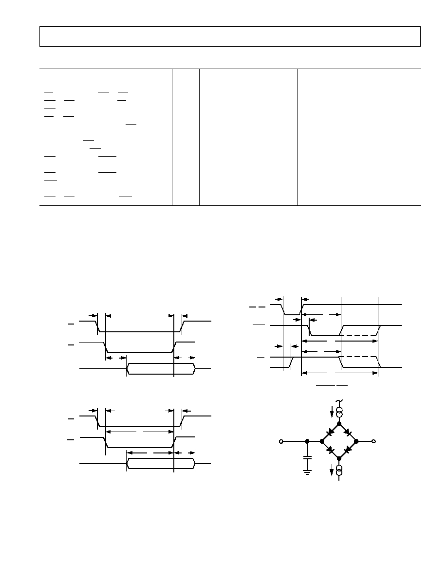
TIMING SPECIFICATIONS
1, 2
(V
CC
= +5 V 5%; AGND = DGND = 0 V; all specifications T
MIN
to T
MAX
unless otherwise noted.)
t
3
t
11
t
10
t
9
t
8
FIRST
CONVERSION
FINISHED
(CR6 = 0)
SECOND
CONVERSION
FINISHED (CR6 = 1)
AD7777/AD7778 ONLY
t
9
BUSY
(CR8 = 0)
INT
(CR8 = 1)
t
10
WR, RD
Figure 3. BUSY/INT Timing
I
OL
1.6mA
+2.1V
I
OH
200
µ
A
C
OUT
100pF
DB n
Figure 4. Load Circuit for Bus Timing Characteristics
t
1
CS
t
2
t
4
t
5
RD
DB0DB9
Figure 1. Read Cycle Timing
t
1
CS
t
2
t
6
WR
DB0DB9
t
3
t
7
Figure 2. Write Cycle Timing
Parameter
Label
Limit at T
MIN
to T
MAX
Units
Test Conditions/Comments
INTERFACE TIMING
CS Falling Edge to WR or RD Falling Edge
t
1
0
ns min
WR or RD Rising Edge to CS Rising Edge
t
2
0
ns min
WR Pulse Width
t
3
53
ns min
CS or RD Active to Valid Data
3
t
4
60
ns max
Timed from Whichever Occurs Last
Bus Relinquish Time after
RD
4
t
5
10
ns min
45
ns max
Data Valid to
WR Rising Edge
t
6
55
ns min
Data Valid after
WR Rising Edge
t
7
10
ns min
WR Rising Edge to BUSY Falling Edge
t
8
1.5 t
CLKIN
ns min
CR9 = 0
2.5 t
CLKIN
+ 70
ns max
WR Rising Edge to BUSY Rising Edge or
INT Falling Edge
t
9
19.5 t
CLKIN
+ 70
ns max
Single Conversion, CR6 = 0
t
10
33.5 t
CLKIN
+ 70
ns max
Double Conversion, CR6 = 1
WR or RD Falling Edge to INT Rising Edge
t
11
60
ns max
CR9 = 1
NOTES
1
See Figures 1 to 3.
2
Timing specifications in bold print are 100% production tested. All other times are guaranteed by design, not production tested. All input signals are specified with
tr = tf = 5 ns (10% to 90% of 5 V) and timed from a voltage level of 1.6 V.
3
t
4
is measured with the load circuit of Figure 4 and defined as the time required for an output to cross 0.8 V or 2.4 V.
4
t
5
is derived from the measured time taken by the data outputs to change 0.5 V when loaded with the circuit of Figure 4. The measured time is then extrapolated back
to remove the effects of charging or discharging the 100 pF capacitor. This means that the time t
5
quoted above is the true bus relinquish time of the device and, as
such, is independent of the external bus loading capacitance.
Specifications subject to change without notice.
AD7776/AD7777/AD7778
4
REV. 0
ABSOLUTE MAXIMUM RATINGS*
(T
A
= +25
°
C unless otherwise noted)
V
CC
to AGND or DGND . . . . . . . . . . . . . . . . . . 0.3 V, +7 V
AGND, RTN to DGND . . . . . . . . . . . . . 0.3 V, V
CC
+ 0.3 V
CS, RD, WR, CLKIN, DB0DB9,
BUSY/INT to DGND . . . . . . . . . . . . . 0.3 V, V
CC
+ 0.3 V
Analog Input Voltage to AGND . . . . . . . 0.3 V, V
CC
+ 0.3 V
REFOUT to AGND . . . . . . . . . . . . . . . . 0.3 V, V
CC
+ 0.3 V
REFIN to AGND . . . . . . . . . . . . . . . . . . 0.3 V, V
CC
+ 0.3 V
Operating Temperature Range
All Versions . . . . . . . . . . . . . . . . . . . . . . . . 40
°
C to +85
°
C
Storage Temperature Range . . . . . . . . . . . . 65
°
C to +150
°
C
Junction Temperature . . . . . . . . . . . . . . . . . . . . . . . . +150
°
C
DIP Package, Power Dissipation . . . . . . . . . . . . . . . . 875 mW
JA
Thermal Impedance . . . . . . . . . . . . . . . . . . . . . 75
°
C/W
Lead Temperature, Soldering (10 sec) . . . . . . . . . . +260
°
C
SOIC Packages, Power Dissipation . . . . . . . . . . . . . . 875 mW
JA
Thermal Impedance . . . . . . . . . . . . . . . . . . . . . 75
°
C/W
Lead Temperature, Soldering
Vapor Phase (60 sec) . . . . . . . . . . . . . . . . . . . . . . +215
°
C
Infrared (15 sec) . . . . . . . . . . . . . . . . . . . . . . . . . +220
°
C
PQFP Package, Power Dissipation . . . . . . . . . . . . . . 500 mW
JA
Thermal Impedance . . . . . . . . . . . . . . . . . . . . . 95
°
C/W
Lead Temperature, Soldering
Vapor Phase (60 sec) . . . . . . . . . . . . . . . . . . . . . . +215
°
C
Infrared (15 sec) . . . . . . . . . . . . . . . . . . . . . . . . . +220
°
C
*Stresses above those listed under "Absolute Maximum Ratings" may cause
permanent damage to the device. This is a stress rating only; functional operation
of the device at these or any other conditions above those listed in the operational
sections of this specification is not implied. Exposure to absolute maximum rating
conditions for extended periods may affect device reliability.
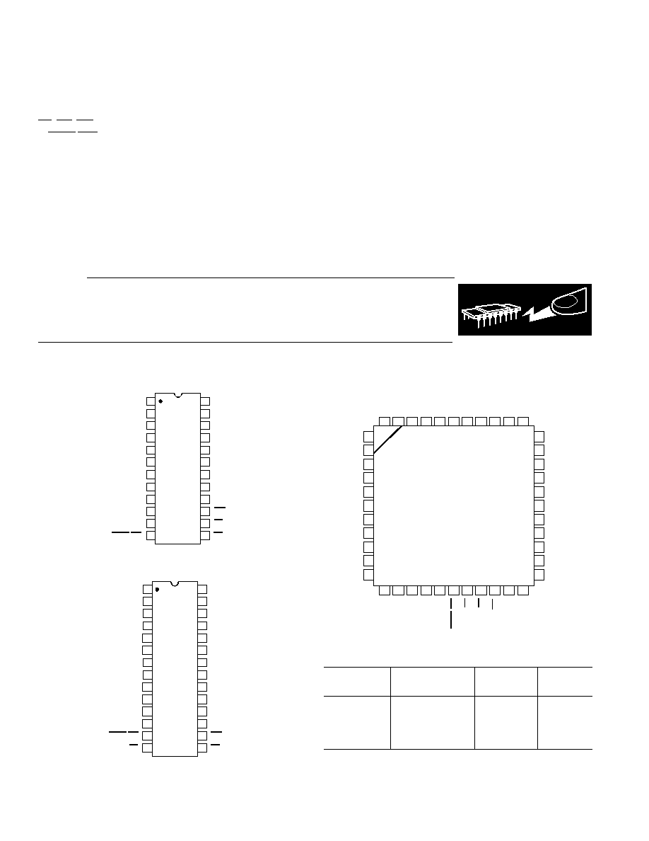
PIN CONFIGURATIONS
WARNING!
ESD SENSITIVE DEVICE
CAUTION
ESD (electrostatic discharge) sensitive device. Electrostatic charges as high as 4000 V readily
accumulate on the human body and test equipment and can discharge without detection. Although
the AD7776/AD7777/AD7778 feature proprietary ESD protection circuitry, permanent damage
may occur on devices subjected to high energy electrostatic discharges. Therefore, proper ESD
precautions are recommended to avoid performance degradation or loss of functionality.
24-Pin SOIC
1
2
24
23
22
10
15
11
12
14
13
21
20
18
17
16
19
9
3
4
5
TOP VIEW
(Not to Scale)
7
8
6
AD7776
DB2
DB3
DGND
DB4
DB5
DB6
DB7
DB1
DB0
C
REFIN
AGND
RTN
REFIN
A
IN
AGND
REFOUT
V
CC
DB8
(MSB) DB9
CLKIN
BUSY/INT
RD
WR
CS
28-Pin DIP & SOIC
1
2
24
23
22
10
15
11
12
14
13
21
20
17
16
9
3
4
5
7
8
6
18
19
TOP VIEW
(Not to Scale)
28
27
26
25
AD7777
NC
NC = NO CONNECT
DB2
DB3
DGND
DB4
DB5
DB6
DB7
DB1
DB0
DB8
(MSB) DB9
BUSY/INT
C
REFIN
AGND
RTN
REFIN
AGND
REFOUT
V
CC
CLKIN
RD
WR
CS
A
IN
4
A
IN
3
A
IN
2
A
IN
1
ORDERING GUIDE
Temperature
No. of
Package
Model
Range
Channels
Option
1
AD7776AR
2
40
°
C to +85
°
C
1
R-24
AD7777AN
40
°
C to +85
°
C
4
N-28
AD7777AR
2
40
°
C to +85
°
C
4
R-28
AD7778AS
2
40
°
C to +85
°
C
8
S-44
NOTES
1
R = SOIC, N = Plastic DIP, S = PQFP.
2
Analog Devices reserves the right to ship devices branded with a J in place of
the A, e.g., AD7776JR instead of AD7776AR. Temperature range remains
40
°
C to +85
°
C.
44-Pin PQFP
7
8
9
10
11
6
5
4
3
2
1
33
32
31
30
29
28
27
26
25
24
23
18
19
20
21
22
17
16
15
14
13
12
39
38
37
36
35
34
44
43
42
41
40
TOP VIEW
(Not to Scale)
AD7778
NC
NC
NC
NC
NC
NC
NC
NC
NC
NC
NC
NC
NC
DB2
DB3
DGND
DB4
DB5
DB6
DB7
DB1
DB0
C
REFIN
RTN
AGND
REFIN
A
IN
8
A
IN
7
A
IN
6
A
IN
5
A
IN
4
A
IN
3
A
IN
2
A
IN
1
AGND
REFOUT
V
CC
DB8
(
MSB) DB9
CLKIN
BUSY/INT
RD
WR
CS
NC = NO CONNECT
AD7776/AD7777/AD7778
5
REV. 0
PIN FUNCTION DESCRIPTION
Mnemonic
Description
V
CC
+5 V Power Supply.
AGND
Analog Ground.
DGND
Digital Ground. Ground reference for digital circuitry.
DB0DB9
Input/Output Data Bus. This is a bidirectional data port from which ADC output data may be read and to which
control register data may be written.
BUSY/INT
Busy/Interrupt Output. Active low logic output indicating A/D converter status. This logic output has two modes
of operation depending on whether location CR9 of the control register has been set low or high:
If CR9 is set low, then the
BUSY/INT output will behave as a BUSY signal. The BUSY signal will go low and stay
low for the duration of a single conversion, or if simultaneous sampling has been selected,
BUSY will stay low for
the duration of both conversions.
If CR9 is set high, then the
BUSY/INT output behaves as an INTERRUPT signal. The INT signal will go low
and remain low after either a single conversion is completed or after a double conversion is completed if simulta-
neous sampling has been selected. With CR9 high, the falling edge of
WR or RD resets the INT line high.
CS
Chip Select Input. The device is selected when this input is low.
WR
Write Input (Active Low). It is used in conjunction with
CS to write data to the control register. Data is latched to the
registers on the rising edge of
WR. Following the rising edge of WR, the analog input is acquired and a conversion is
started.
RD
Read Input (Active Low). It is used in conjunction with
CS to enable the data outputs from the ADC registers.
A
IN
18
Analog Inputs 18. The analog input range is V
BIAS
±
V
SWING
where V
BIAS
and V
SWING
are defined by the reference
voltage applied to REFIN. Input resistance between any of the analog input pins and AGND is 10 k
or greater.
REFIN
Voltage Reference Input. The AD7776/AD7777/AD7778 are specified over a voltage reference range of 1.9 V to 2.1 V
with a nominal value of 2.0 V. This REFIN voltage provides the V
BIAS
and V
SWING
levels for the input channel(s).
V
BIAS
is equal to REFIN and V
SWING
is nominally equal to REFIN/2. Input resistance between this REFIN pin and
AGND is 10 k
or greater.
REFOUT
Voltage Reference Output. The internal voltage reference, which is nominally 2.0 V and can be used to provide the
bias voltage (V
BIAS
) for the input channel(s), is provided at this pin.
C
REFIN
Reference Decoupling Capacitor. A 10 nF capacitor must be connected from this pin to AGND to ensure correct
operation of the high speed ADC.
RTN
Signal Return Path for the input channel(s). Normally RTN is connected to AGND at the package.
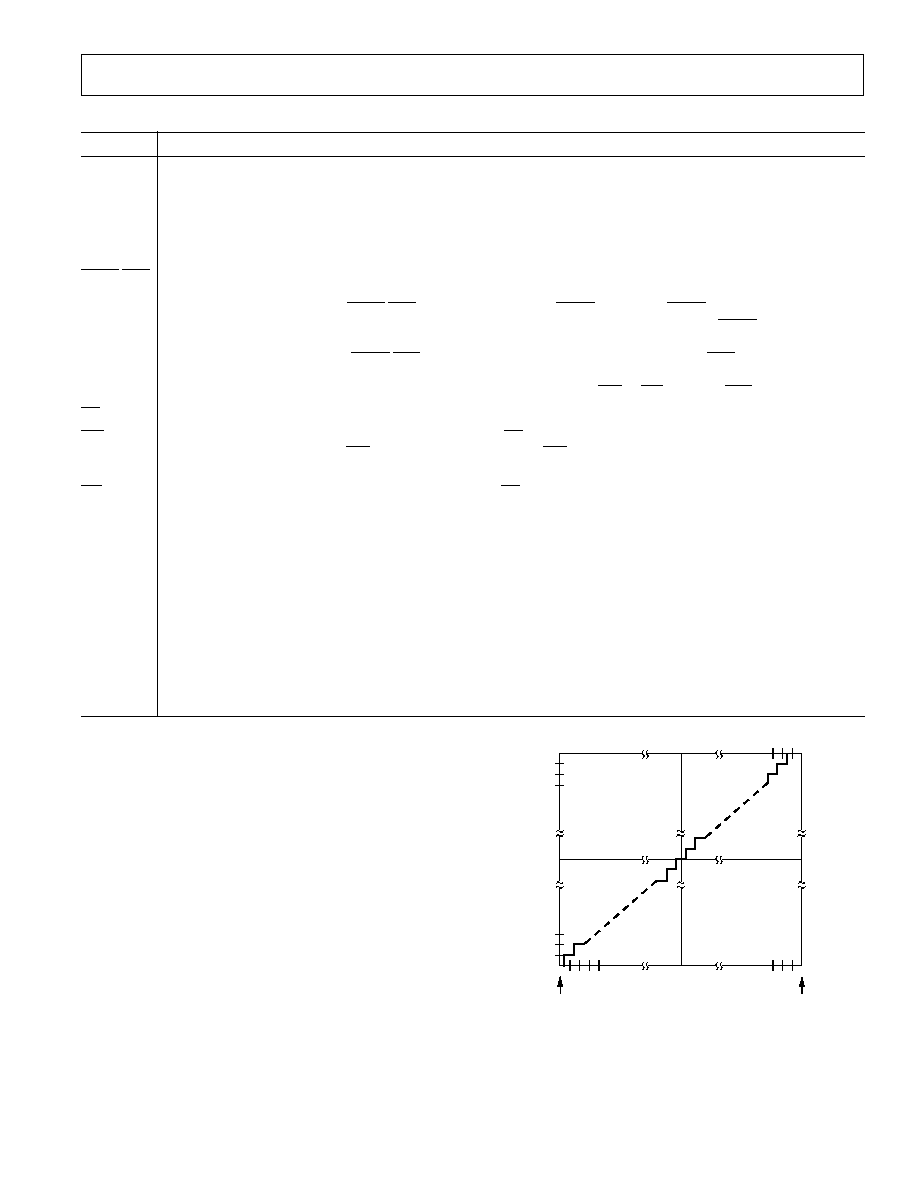
CIRCUIT DESCRIPTION
ADC Transfer Function
For all versions, an input signal of the form V
BIAS
±
V
SWING
is
expected. This V
BIAS
signal level operates as a pseudo ground to
which all input signals must be referred. The V
BIAS
level is de-
termined by the voltage applied to the REFIN pin. This can be
driven by an external voltage source or, alternatively, the on-
board 2 V reference, available at REFOUT, can be used. The
magnitude of the input signal swing is equal to V
BIAS
/2 (or
REFIN/2) and is set internally. With a REFIN of 2 V, the analog
input signal level varies from 1 V up to 3 V i.e., 2
±
1 V. Fig-
ure 5 shows the transfer function of the ADC and its relation-
ship to V
BIAS
and V
SWING
. The half-scale twos complement code
of the ADC, 000 Hex (00 0000 0000 Binary), occurs at an input
voltage equal to V
BIAS
. The input full-scale range of the ADC is
equal to 2 V
SWING
, so that the Plus Full-Scale transition (1FE to
1FF) occurs at a voltage equal to V
BIAS
+ V
SWING
1.5 LSBs
and the minus full-scale code transition (200 to 201) occurs at
a voltage V
BIAS
V
SWING
+ 0.5 LSBs.
ADC
OUTPUT
CODE
(HEX)
1FF
1FE
202
201
200
000
V
BIAS
V
SWING
V
BIAS
V
BIAS
+V
SWING
ANALOG INPUT, V
IN
Figure 5. ADC Transfer Function

AD7776/AD7777/AD7778
6
REV. 0
CR6: Determines whether operation is on a single channel or
simultaneous sampling on two channels. Location CR6 is a
"don't care" for the AD7776.
CR6
Function
0
Single channel operation. Channel select
address is contained in locations CR0CR2.
1
Two channels simultaneously sampled
and sequentially converted. Channel
select addresses contained in locations
CR0CR2 and CR3CR5.
CR7: Determines whether the device is in the normal operating
mode or in the half-scale test mode.
CR7
Function
0
Normal Operating Mode
1
Half-Scale Test Mode
In the half-scale test mode REFIN is internally connected as an
analog input(s). In this mode locations CR0CR2 and CR3
CR5 are all "don't cares" since it is REFIN which will be con-
verted. For the AD7777 and AD7778, the contents of location
CR6 still determine whether a single or a double conversion is
carried out on the REFIN level.
CR8: Determines whether the device is in the normal operating
mode or in the powerdown mode.
CR8
Function
0
Normal Operating Mode
1
Powerdown Mode
In the powerdown mode all linear circuitry is turned off and the
REFOUT output is weakly (5 k
) pulled to AGND. The input
impedance of the analog inputs and of the REFIN input re-
mains the same in either normal mode or powerdown mode. See
under Circuit Description--Powerdown Mode.
CR9: Determines whether
BUSY/INT output flag goes low and
remains low during conversion(s) or else goes low and remains
low after the conversion(s) is (are) complete.
CR9
BUSY/INT Functionality
0
Output goes low and remains low during
conversion(s).
1
Output goes low and remains low after conversion(s)
is (are) complete.
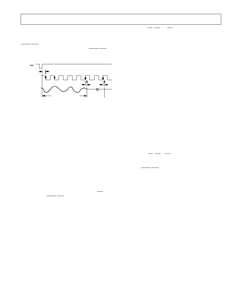
ADC Conversion Start Timing
Figure 6 shows the operating waveforms for the start of a con-
version cycle. On the rising edge of
WR, the conversion cycle
starts with the acquisition and tracking of the selected ADC
channel, A
IN
18. The analog input voltage is held 40 ns (typi-
cally) after the first rising edge of CLKIN following four com-
plete CLKIN cycles. If t
D
in Figure 6 is greater than 12 ns, the
falling edge of CLKIN as shown will be seen as the first falling
clock edge. If t
D
is less than 12 ns, the first falling clock edge to
be recognized will not occur until one cycle later.
Following the "hold" on the analog input(s), two complete
CLKIN cycles are allowed for settling purposes before the MSB
decision is made. The actual decision point occurs approximately
40 ns after the rising edge of CLKIN as shown in Figure 6. A
further two CLKIN cycles are allowed for the second MSB
decision. The succeeding bit decisions are made approximately
40 ns after each rising edge of CLKIN until the conversion is
complete. At the end of conversion, if a single conversion
has been requested (CR6 = 0), the
BUSY/INT line changes
CONTROL REGISTER
The control register is 10-bits wide and can only be written to.
On power-on, all locations in the control register are automati-
cally loaded with 0s. For the single channel AD7776, locations
CR0 to CR6 of the control register are "don't cares." For the
quad channel AD7777, locations CR2 and CR5 are "don't
cares." Individual bit functions are described below.
CR0CR2: Channel Address Locations. Determines which channel
will be selected and converted for single channel operation. For si-
multaneous sampling operation CR0CR2 holds the address of one
of the two channels to be sampled.
AD7776
CR2 CR1
CR0
Function
X*
X
X
Select A
IN
1
*X = Don't Care
AD7777
CR2 CR1
CR0
Function
X*
0
0
Select A
IN
1
X
0
1
Select A
IN
2
X
1
0
Select A
IN
3
X
1
1
Select A
IN
4
*X = Don't Care
AD7778
CR2 CR1
CR0
Function
0
0
0
Select A
IN
1
0
0
1
Select A
IN
2
0
1
0
Select A
IN
3
0
1
1
Select A
IN
4
1
0
0
Select A
IN
5
1
0
1
Select A
IN
6
1
1
0
Select A
IN
7
1
1
1
Select A
IN
8
CR3CR5: Channel Address Locations. Only applicable for simul-
taneous sampling with the AD7777 or AD7778 when CR3CR5
holds the address of the second channel to be sampled.
AD7777
CR5 CR4
CR3
Function
X*
0
0
Select A
IN
1
X
0
1
Select A
IN
2
X
1
0
Select A
IN
3
X
1
1
Select A
IN
4
*X = Don't Care
AD7778
CR5 CR4
CR3
Function
0
0
0
Select A
IN
1
0
0
1
Select A
IN
2
0
1
0
Select A
IN
3
0
1
1
Select A
IN
4
1
0
0
Select A
IN
5
1
0
1
Select A
IN
6
1
1
0
Select A
IN
7
1
1
1
Select A
IN
8
AD7776/AD7777/AD7778
7
REV. 0
state (as programmed by CR9), and the SAR contents are trans-
ferred to the first register ADCREG1. The SAR is then reset in
readiness for a new conversion. If simultaneous sampling has
been requested (CR6 = 1), no change occurs in the status of the
BUSY/INT output and the ADC automatically starts the second
conversion. At the end of this conversion the
BUSY/INT line
changes state (as programmed by CR9) and the SAR contents
are transferred to the second register, ADCREG2.
t
D
*
CLKIN
V
IN
WR
CHANNEL ACQUISITION
40ns
TYP
40ns
TYP
'HOLD'
DB9 (MSB)
*
TIMING SHOWN FOR t
D
GREATER THAN 12ns
Figure 6. ADC Conversion Start Timing
Track-and-Hold
The track-and-hold (T/H) amplifiers on the analog input(s) of
the AD7776/AD7777/AD7778 allow the ADC to accurately
convert an input sine wave of 2 V peak-peak amplitude up to a
frequency of 189 kHz, the Nyquist frequency of the ADC when
operated at its maximum throughput rate of 378 kHz. This
maximum rate of conversion includes conversion time and time
between conversions. Because the input bandwidth of the track-
and-hold is much greater than 189 kHz, the input signal should
be band limited to avoid folding unwanted signals into the band
of interest.
Powerdown
The AD7776/AD7777/AD7778 can be placed in a powerdown
mode simply by writing a logic high to location CR8 of the con-
trol register. The following changes are effected immediately on
writing a "1" to location CR8:
· Any conversion in progress is terminated.
· If a conversion is in progress, the leading edge of
WR immedi-
ately drives the
BUSY/INT output high.
· All the linear circuitry is turned off.
· The REFOUT output stops being driven and is weakly (5 k
)
pulled to analog ground.
Control inputs
CS, WR and RD retain their purpose while the
AD7776/ AD7777/AD7778 is in powerdown. If no conversions
are in progress when the AD7776/AD7777/AD7778 is placed
into the powerdown modes, the contents of the ADC registers,
ADCREG1 and ADCREG2, are retained during powerdown
and can be read as normal. On returning to normal operating
mode a new conversion (or conversions, dependent on CR6) is
automatically started. On completion, the invalid conversion
results are loaded into the ADC registers losing the previous
valid results.
In order to achieve the lowest possible power consumption in
the powerdown mode special attention must be paid to the state
of the digital and analog inputs and outputs:
· Because each analog input channel sees a resistive divider to
AGND, the input resistance of which does not change be-
tween normal and powerdown modes, driving the analog input
signals to 0 V or as close as possible to 0 V will minimize the
power dissipated in the input signal conditioning circuitry.
· Similarly, the REFIN input sees a resistive divider to AGND,
the input resistance of which does not change between normal
and powerdown modes. If an external reference is being used,
then driving this reference input to 0 V or as close as possible
to 0 V will minimize the power dissipated in the input signal
conditioning circuitry.
· Since the REFOUT pin is pulled to AGND via, typically, a
5 k
resistor, any voltage above 0 V that this output may be
pulled to by external circuitry will dissipate unnecessary
power.
· Digital inputs CS, WR & RD should all be held at V
CC
or as
close as possible. CLKIN should be held as close as possible
to either 0 V or V
CC.
· Since the
BUSY/INT output is actively driven to a logic high,
any loading on this pin to 0 V will dissipate power.
The AD7776/AD7777/AD7778 comes out of the powerdown
mode when a Logic "0" is written to location CR8 of the con-
trol register. Note that the contents of the other locations in the
control register are retained when the device is placed in
powerdown and are valid when power is restored. However,
coming out of powerdown provides an opportunity to reload
the complete contents of the control register without any extra
instructions.
AD7776/AD7777/AD7778
8
REV. 0
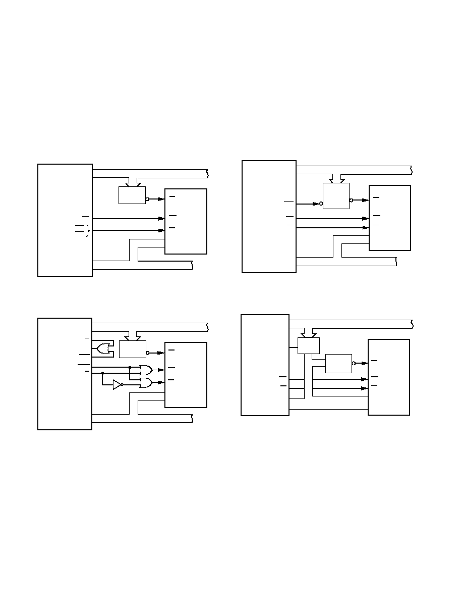
Microprocessor Interfacing Circuits
The AD7776/AD7777/AD7778 family of ADCs is intended to
interface to DSP machines such as the ADSP-2101, ADSP-2105,
the TMS320 family and microcontrollers such as the 80C196
family.
Figure 7 shows the AD7776/AD7777/AD7778 interfaced to the
TMS320C10 @ 20.5 MHz and the TMS320C14 @ 25 MHz.
Figure 8 shows the interface with the TMS320C25 @ 40 MHz.
Note that one wait state is required with this interface. The
ADSP-2101-50 and the ADSP-2105-40 interface is shown in
Figure 9. One wait state is required with either of these machines.
*
ADDITIONAL PINS OMITTED FOR CLARITY
ADDR
DECODE
ADDRESS BUS
DATA BUS
D15D0
TMS320C10-20.5
TMS320C14-25
A11A0
WE
(C10) DEN
(C14) REN
CS
DB9DB0
AD7776/7/8*
RD
WR
Figure 7. AD7776/AD7777/AD7778 to TMS320C10 and
TMS320C14 Interface
ADDRESS BUS
DATA BUS
*
ADDITIONAL PINS OMITTED FOR CLARITY
CS
DB9DB0
AD7776/7/8*
RD
WR
ADDR
DECODE
D15D0
A15A0
IS
READY
MSC
STRB
R/W
TMS320C25-40
Figure 8. AD7776/AD7777/AD7778 to TMS320C25 Interface
Figure 10 shows the interface with the 80C196KB @ 12 MHz
and the 80C196KC @ 16 MHz. One wait state is required with
the 16 MHz machine. The 80C196 is configured to operate
with a 16-bit multiplexed address/data bus.
Table I gives a truth table for the AD7776/AD7777/AD7778
and summarizes their microprocessor interfacing features. Note
that a read instruction to any of the devices while a conversation
is in progress will immediately stop that conversion and return
unreliable data over the data bus.
*
ADDITIONAL PINS OMITTED FOR CLARITY
ADDRESS BUS
DATA BUS
CS
DB9DB0
AD7776/7/8*
RD
WR
D23D6
A13A0
WR
RD
DMS
ADSP-2101-50
ADSP-2105-40
ADDR
DECODE
EN
Figure 9. AD7776/AD7777/AD7778 to ADSP-2101 and
ADSP-2105 Interface
*
ADDITIONAL PINS OMITTED FOR CLARITY
DATA BUS (10)
CS
DB9DB0
AD7776/7/8*
RD
WR
ADDR
DECODER
'373
LATCH
ADDRESS BUS
AD7AD0
(PORT 3)
AD15AD6
(PORT 4)
WR
RD
80C196KB-12
80C196KC-16
ALE
Figure 10. AD7776/AD7777/AD7778 to 80C196 Interface

AD7776/AD7777/AD7778
9
REV. 0
Table I. AD7776/AD7777/AD7778 Truth Table for Microprocessor Interfacing
CS
RD
WR
DB0DB9
Function/Comments
1
X*
X*
High Z
Data Port High Impedance
0
1
j
CR Data
Load control register (CR) data to control register and start a conversion.
0
k
1
ADC Data
ADC data placed on data bus. Depending upon location CR6 of the control register, one or two
Read instructions will be required.
If CR6 is low, i.e., single channel conversion selected, a read instruction returns the contents of
ADCREG1. Succeeding read instructions continue to return the contents of ADCREG1.
If CR6 is high, i.e., simultaneous sampling (double conversion) selected, the first read instruction
returns the contents of ADCREG1 while the second read instruction returns the contents of
ADCREG2. A third read instruction returns ADCREG1 again, the fourth ADCREG2, etc.
*X = Don't Care
DESIGN INFORMATION
Layout Hints
Ensure that the layout for the printed circuit board has the digi-
tal and analog grounds separated as much as possible. Take care
not to run any digital track alongside an analog signal track.
Guard (screen) the analog input(s) with RTN.
Establish a single point analog ground separate from the logic
system ground and as close as possible to the AD7776/AD7777/
AD7778. Both the RTN and AGND pins on the AD7776/
AD7777/AD7778 and all other signal grounds should be con-
nected to this single point analog ground. In turn, this star
ground should be connected to the digital ground at one point
only--preferably at the low impedance power supply itself.
Low impedance analog and digital power supply common re-
turns are important for correct operation of the devices, so make
the foil width for these tracks as wide as possible.
In order to ensure a low impedance +5 V power supply at the
actual V
CC
pin, it will be necessary to employ bypass capacitors
from the pin itself to DGND. A 4.7
µ
F tantalum capacitor in
parallel with a 0.1
µ
F ceramic capacitor is sufficient.
ADC Corruption
Executing a read instruction to the AD7776/AD7777/AD7778
while a conversion is in progress will immediately halt the con-
version and return invalid data over the data bus. The
BUSY/
INT output pin should be monitored closely and all read in-
structions to the AD7776/AD7777/AD7778 prevented while
this output shows that a conversion is in progress.
Executing a write instruction to the AD7776/AD7777/AD7778
while a conversion is in progress immediately halts the conver-
sion, the falling edge of
WR driving the BUSY/INT output high.
The analog input(s) is sampled as normal and a new conversion
sequence (dependent upon CR6) is started.
ADC Conversion Time
Although each conversion takes only 14 CLKIN cycles, it can
take between 4.5 to 5.5 CLKIN cycles to acquire the analog
input(s) after the
WR input goes high and before any conver-
sions start.
TERMINOLOGY
Relative Accuracy
For the AD7776, AD7777 and AD7778, relative accuracy or
endpoint nonlinearity is the maximum deviation, in LSBs, of the
ADC's actual code transition points from a straight line drawn
between the endpoints of the ADC transfer function.
Differential Nonlinearity
Differential nonlinearity is the difference between the measured
change and the ideal 1 LSB change between any two adjacent
codes. A specified maximum differential nonlinearity of
±
1 LSB
ensures no missed codes.
Bias Offset Error
For an ideal 10-bit ADC, the output code for an input voltage
equal to V
BIAS
should be midscale. The bias offset error is the
difference between the actual midpoint voltage for midscale
code and V
BIAS
, expressed in LSBs.
Bias Offset Error Match
This is a measure of how closely the bias offset errors of all
channels track each other. The bias offset error match of any
channel must be no further away than 10 LSBs from the bias
offset error of any other channel, regardless of whether the
channels are independently sampled or simultaneously sampled.
Plus and Minus Full-Scale Error
The input channels of the ADC can be considered to have
bipolar (positive and negative) input ranges, but which are re-
ferred to V
BIAS
(or REFIN) instead of AGND. Positive full-scale
error for the ADC is the difference between the actual input
voltage required to produce the plus full-scale code transition
and the ideal input voltage (V
BIAS
+ V
SWING
1.5 LSB), ex-
pressed in LSBs. Minus full-scale error is similarly specified for
the minus full-scale code transition, relative to the ideal input
voltage for this transition (V
BIAS
V
SWING
+ 0.5 LSB). Note that
the full-scale errors for the ADC input channels are measured
after their respective bias offset errors have been adjusted out.
Plus and Minus Full-Scale Error Match
This is a measure of how closely the full-scale errors of all chan-
nels track each other. The full-scale error match of any channel
must be no further away than 10 LSBs from the respective full-
scale error of any other channel, regardless of whether the chan-
nels are independently sampled or simultaneously sampled.
AD7776/AD7777/AD7778
10
REV. 0
Short Circuit Current
This is defined as the maximum current which will flow either
into or out of the REFOUT pin if this pin is shorted to any
potential between 0 V and V
CC
. This condition can be allowed
for up to 10 seconds provided that the power dissipation of the
package is not exceeded.
Signal-to-Noise and Distortion Ratio, S/(N+D)
Signal-to-noise and distortion ratio, S/(N+D), is the ratio of the
rms value of the measured input signal to the rms sum of all
other spectral components below the Nyquist frequency, includ-
ing harmonics but excluding dc. The value for S/(N+D) is given
in decibels.
Total Harmonic Distortion, THD
Total harmonic distortion is the ratio of the rms sum of the first
five harmonic components to the rms value of a full-scale input
signal and is expressed in decibels. For the AD7776/AD7777/
AD7778, total harmonic distortion (THD) is defined as:
(V
2
2
+ V
3
2
+ V
4
2
+ V
5
2
+ V
6
2
)
1/2
20 log =
V
1
where V
1
is the rms amplitude of the fundamental and V
2
,
V
3
, V
4
, V
5
and V
6
are the rms amplitudes of the individual
harmonics.
Intermodulation Distortion, IMD
With inputs consisting of sine waves at two frequencies, fa and
fb, any active device with nonlinearities will create distortion
products, of order (m + n), at sum and difference frequencies of
mfa + nfb, where m, n = 0, 1, 2, 3. Intermodulation terms are
those for which m or n is not equal to zero. For example, the
second order terms include (fa + fb) and (fa fb) and the third
order terms include (2 fa + fb), (2 fa fb), (fa + 2 fb) and (fa
2 fb).
Channel-to-Channel Isolation
Channel-to-channel isolation is a measure of the level of cross-
talk between channels. It is measured by applying a full-scale
100 kHz sine wave signal to any one of the input channels and
monitoring the remaining channels. The figure given is the
worst case across all channels.
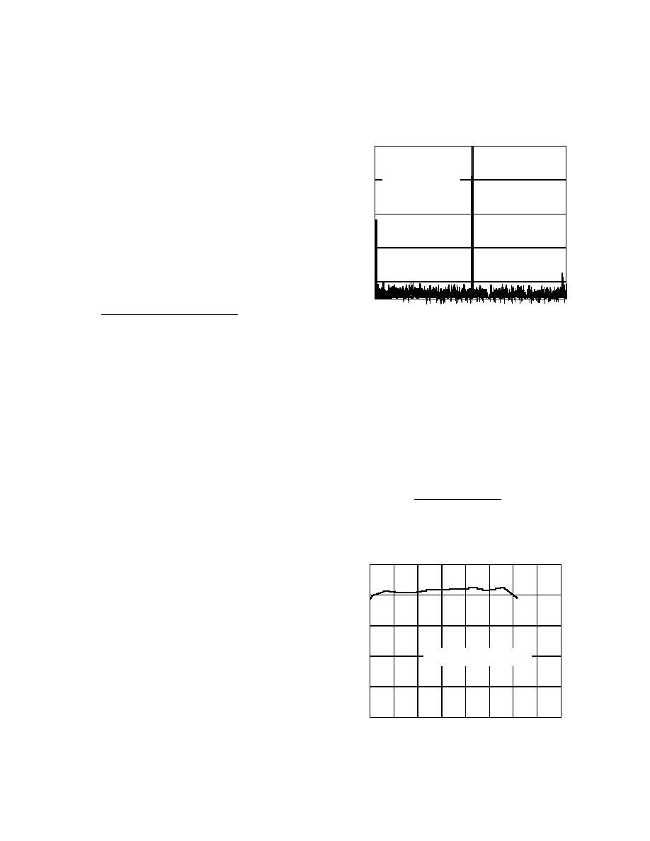
DIGITAL SIGNAL PROCESSING APPLICATIONS
In digital signal processing (DSP) application areas like voice
recognition, echo cancellation and adaptive filtering, the dy-
namic characteristics S/(N+D), THD & IMD of the ADC are
critical. The AD7776/AD7777/AD7778 are specified dynami-
cally as well as with standard dc specifications. Because the
track/hold amplifier has a wide bandwidth, an antialiasing filter
should be placed on the analog inputs to avoid aliasing of high
frequency noise back into the bands of interest.
The dynamic performance of the ADC is evaluated by applying
a sine wave signal of very low distortion to a single analog input
which is sampled at a 380.95 kHz sampling rate. A fast Fourier
transform (FFT) plot or histogram plot is then generated from
which the signal to noise and distortion, harmonic distortion
and dynamic differential nonlinearity data can be obtained.
Similarly, for intermodulation distortion, an input signal con-
sisting of two pure sine waves at different frequencies is applied
to the AD7776/AD7777/AD7778.
Figure 11 shows a 2048 point FFT plot for a single channel of
the AD7778 with an input signal of 99.88 kHz. The SNR is
58.71 dB. It can be seen that most of the harmonics are buried
in the noise floor. It should be noted that the harmonics are
taken into account when calculating the S/(N+D).
0
90
80
0
60
40
20
99.88
SIGNAL AMPLITUDE dB
FREQUENCY kHz
INPUT FREQUENCY =
99.88 kHz
SAMPLE FREQUENCY =
380.95 kHz
SNR = 58.7 dB
T
A
= +25
°
C
Figure 11. ADC FFT Plot
The relationship between S/(N+D) and resolution (n) is ex-
pressed by the following equation:
S/(N+D) = (6.02n + 1.76) dB
This is for an ideal part with no differential or integral linearity
errors. These errors will cause a degradation in S/(N+D). By
working backwards from the above equation, it is possible to get
a measure of ADC performance expressed in effective number
of bits (n).
S/(N+D) (dB) 1.76
n(effective) =
6.02
The effective number of bits plotted vs. frequency for a single
channel of the AD7778 is shown in Figure 12. The effective
number of bits is typically 9.5.
10
7.5
189.2
9
8
8.5
0
9.5
INPUT FREQUENCY kHz
EFFECTIVE NUMBER OF BITS
SAMPLE FREQUENCY = 378.4 kHz
T
A
= +24
°
C
Figure 12. Effective Number of Bits vs. Frequency
AD7776/AD7777/AD7778
11
REV. 0
RTN is tied to REFOUT then the analog input range becomes
0 V to 2 V. The fixed 2 V analog input voltage span of the ADC
can range from 1 V to 3 V (RTN = 0 V) to 0 V to 2 V (RTN =
2 V), i.e., with proper biasing, an input signal range from 0.3 V
to 2.3 V can be covered. Both the relative accuracy and differen-
tial nonlinearity performance remains essentially unchanged in
this mode while the SNR and THD performance are typically
2 dB to 3 dB worse than standard.
Changing the Analog Input Voltage Range
By biasing the RTN pin above AGND it is possible to change
the analog input voltage range from its V
BIAS
±
V
SWING
format to
a more traditional 0 V to V
REF
range. The new input range can
be described as
V
OFFSET
to (V
OFFSET
+ REFIN)
where 0 V
V
OFFSET
1 V. To produce this range the RTN pin
must be biased to (REFIN 2 V
OFFSET
). For instance if
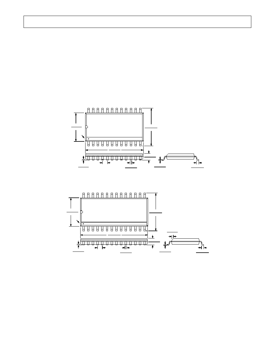
OUTLINE DIMENSIONS
Dimensions shown in inches and (mm).
R-24
24-Lead Wide-Body SOIC
PIN 1
0.299 (7.6)
0.291 (7.4)
13
12
1
24
0.419 (10.65)
0.394 (10.00)
0.013 (0.32)
0.009 (0.23)
0.005 (1.27)
0.015 (0.40)
0.614 (15.6)
0.598 (15.2)
0.104 (2.65)
0.093 (2.35)
0.012 (0.3)
0.004 (0.1)
0.019 (0.49)
0.014 (0.35)
0.050 (1.27)
BSC
R-28
28-Lead Wide-Body SOIC
PIN 1
0.299 (7.60)
0.291 (7.39)
15
14
1
28
0.414 (10.52)
0.398 (10.10)
0.03 (0.76)
0.02 (0.51)
0.013 (0.32)
0.009 (0.23)
0.042 (1.067)
0.018 (0.457)
0.708 (18.02)
0.696 (17.67)
0.096 (2.44)
0.089 (2.26)
0.01 (0.254)
0.006 (0.15)
0.019 (0.49)
0.014 (0.35)
0.050 (1.27)
BSC
1. LEAD NO. 1 IDENTIFIED BY A DOT.
2. SOIC LEADS WILL BE EITHER TIN PLATED OF SOLDER DIPPED
IN ACCORDANCE WITH MIL-M-38510 REQUIREMENTS.

AD7776/AD7777/AD7778
12
REV. 0
OUTLINE DIMENSIONS
Dimensions shown in inches and (mm).
C1762241/93
PRINTED IN U.S.A.
N-28
28-Lead Plastic DIP
PIN 1
0.550 (13.97)
0.530 (13.462)
1
14
15
28
0.606 (15.39)
0.594 (15.09)
0.012 (0.305)
0.008 (0.203)
0.160 (4.06)
0.140 (3.56)
15
°
0
°
0.200
(5.080)
MAX
0.020 (0.508)
0.015 (0.381)
SEATING
PLANE
1.450 (36.83)
1.440 (36.576)
0.105 (2.67)
0.095 (2.41)
0.065 (1.65)
0.045 (1.14)
0.175 (4.45)
0.120 (3.05)
S-44
44-Pin PQFP
1
44
34
33
23
22
12
11
TOP VIEW
PIN 1
0.014 ± 0.002
(0.35 ± 0.05)
0.031 ± 0.002
(0.8 ± 0.05)
4°± 4°
0.096 (2.45) MAX
0.031 ± 0.006
(0.8 ± 0.15)
0.394 ± 0.004
(10 ± 0.1)
0.079 + 0.004/0.002
(2 + 0.1/0.05)
0.036 ± 0.004
(0.92 ± 0.1)
0.036 ± 0.004
(0.92 ± 0.1)
0.394 ± 0.004 SQ
(10 ± 0.1)
0.547 ± 0.01 SQ
(13.9 ± 0.25)