Äîêóìåíòàöèÿ è îïèñàíèÿ www.docs.chipfind.ru
REV. 0
Information furnished by Analog Devices is believed to be accurate and
reliable. However, no responsibility is assumed by Analog Devices for its
use, nor for any infringements of patents or other rights of third parties
which may result from its use. No license is granted by implication or
otherwise under any patent or patent rights of Analog Devices.
a
AD7741/AD7742
One Technology Way, P.O. Box 9106, Norwood, MA 02062-9106, U.S.A.
Tel: 781/329-4700
World Wide Web Site: http://www.analog.com
Fax: 781/326-8703
© Analog Devices, Inc., 1999
Single and Multichannel, Synchronous
Voltage-to-Frequency Converters
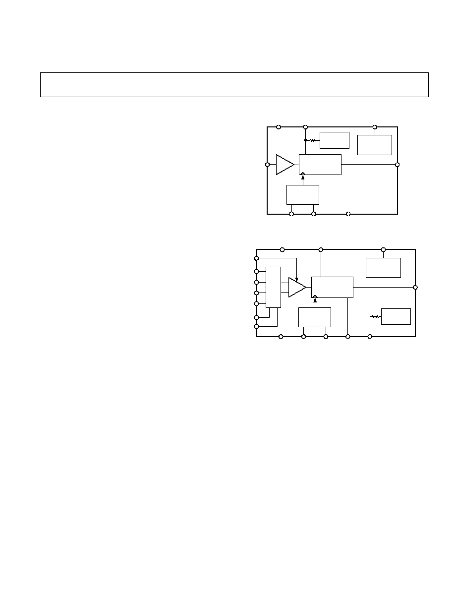
FUNCTIONAL BLOCK DIAGRAMS
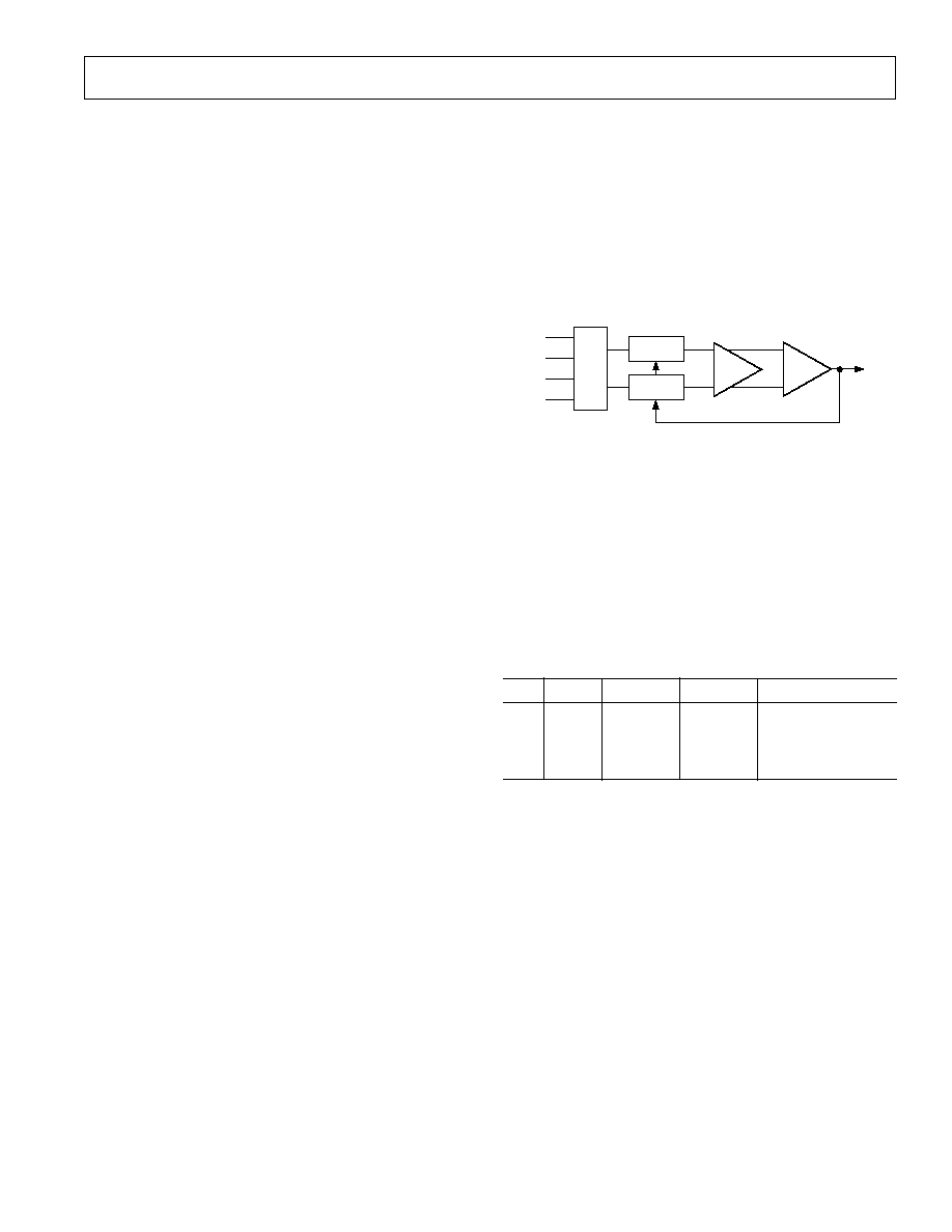
X1
VOLTAGE-TO-
FREQUENCY
MODULATOR
CLOCK
GENERATION
CLKIN
CLKOUT
GND
V
IN
POWER-DOWN
LOGIC
PD
REFIN/OUT
V
DD
f
OUT
AD7741
+2.5V
REFERENCE
X1/X2
INPUT
MUX
VOLTAGE-TO-
FREQUENCY
MODULATOR
REFIN
+2.5V
REFERENCE
REFOUT
CLOCK
GENERATION
CLKIN
CLKOUT
GND
GAIN
V
IN
1
A1
A0
V
IN
2
V
IN
3
V
IN
4
POWER-DOWN
LOGIC
PD
UNI/
BIP
V
DD
f
OUT
AD7742
FEATURES
AD7741: One Single-Ended Input Channel
AD7742: Two Differential or Three Pseudo-Differential
Input Channels
Integral Nonlinearity of 0.012% at f
OUT
(Max) = 2.75 MHz
(AD7742) and at f
OUT
(Max) = 1.35 MHz (AD7741)
Single +5 V Supply Operation
Buffered Inputs
Programmable Gain Analog Front-End
On-Chip +2.5 V Reference
Internal/External Reference Option
Power Down to 35 A Max
Minimal External Components Required
8-Lead and 16-Lead DIP and SOIC Packages
APPLICATIONS
Low Cost Analog-to-Digital Conversion
Signal Isolation
GENERAL DESCRIPTION
The AD7741/AD7742 are a new generation of synchronous
voltage-to-frequency converters (VFCs). The AD7741 is a
single-channel version in an 8-lead package (SOIC/DIP) and the
AD7742 is a multichannel version in a 16-lead package (SOIC/
DIP). No user trimming is required to achieve the specified
performance.
The AD7741 has a single buffered input whereas the AD7742
has four buffered inputs that may be configured as two fully-
differential inputs or three pseudo-differential inputs. Both parts
include an on-chip +2.5 V bandgap reference that provides the
user with the option of using this internal reference or an exter-
nal reference.
The AD7741 has a single-ended voltage input range from 0 V
to REFIN. The AD7742 has a differential voltage input range
from V
REF
to +V
REF
. Both parts operate from a single +5 V
supply consuming typically 6 mA, and also contain a power-
down feature that reduces the current consumption to less than
35
µ
A.

REV. 0
2
AD7741SPECIFICATIONS
(V
DD
= +4.75 V to +5.25 V; V
REF
= +2.5 V; f
CLKIN
= 6.144 MHz; all specifications T
MIN
to
T
MAX
unless otherwise noted.)
B and Y Version
1
Parameter
2
Min
Typ
Max
Units
Conditions/Comments
DC PERFORMANCE
Integral Nonlinearity
f
CLKIN
= 200 kHz
3
±
0.012
% of Span
4
f
CLKIN
= 3 MHz
3
±
0.012
% of Span
f
CLKIN
= 6.144 MHz
±
0.024
% of Span
V
DD
> 4.8 V
Offset Error
±
40
mV
Gain Error
0
+0.8
+1.6
% of Span
Offset Error Drift
3
±
30
µ
V/
°
C
Gain Error Drift
3
±
16
ppm of Span/
°
C
Power Supply Rejection Ratio
3
63
dB
V
DD
=
±
5%
ANALOG INPUT
5
Input Current
±
50
±
100
nA
Input Voltage Range
0
V
REF
V
+2.5 V REFERENCE (REFIN/OUT)
REFIN
Nominal Input Voltage
2.5
V
Input Impedance
6
N/A
REFOUT
Output Voltage
2.38
2.50
2.60
V
Output Impedance
3
1
k
Reference Drift
3
±
50
ppm/
°
C
Line Rejection
60
dB
Reference Noise (0.1 Hz to 10 Hz)
3
100
µ
V p-p
LOGIC OUTPUT
Output High Voltage, V
OH
4.0
V
Output Sourcing 800
µ
A
7
Output Low Voltage, V
OL
0.4
V
Output Sinking 1.6 mA
7
Minimum Output Frequency
0.05 f
CLKIN
Hz
V
IN
= 0 V
Maximum Output Frequency
0.45 f
CLKIN
Hz
V
IN
= V
REF
LOGIC INPUT
PD ONLY
Input High Voltage, V
IH
2.4
V
Input Low Voltage, V
IL
0.8
V
Input Current
±
100
nA
Pin Capacitance
6
10
pF
CLKIN ONLY
Input High Voltage, V
IH
3.5
V
Input Low Voltage, V
IL
0.8
V
Input Current
±
2
µ
A
Pin Capacitance
6
10
pF
CLOCK FREQUENCY
Input Frequency
6.144
MHz
For Specified Performance
POWER REQUIREMENTS
V
DD
4.75
5.25
V
I
DD
(Normal Mode)
8
mA
Output Unloaded
I
DD
(Power-Down)
15
35
µ
A
Power-Up Time
3
30
µ
s
Coming Out of Power-Down Mode
NOTES
1
Temperature ranges: B Version 40
°
C to +85
°
C: Y Version: 40
°
C to +105
°
C.
2
See Terminology.
3
Guaranteed by design and characterization, not production tested.
4
Span = Maximum Output FrequencyMinimum Output Frequency.
5
The absolute voltage on the input pin must not go more positive than V
DD
2.25 V or more negative than GND.
6
Because this pin is bidirectional, any external reference must be capable of sinking/sourcing 400
µ
A in order to overdrive the internal reference.
7
These logic levels apply to CLKOUT only when it is loaded with one CMOS load.
Specifications subject to change without notice.

REV. 0
3
AD7741/AD7742
(V
DD
= +4.75 V to +5.25 V; V
REF
= +2.5 V; f
CLKIN
= 6.144 MHz; all specifications T
MIN
to
T
MAX
unless otherwise noted.)
B Version
1
Y Version
2
Parameter
3
Min
Typ
Max
Min
Typ
Max
Units
Conditions/Comments
DC PERFORMANCE
Integral Nonlinearity
f
CLKIN
= 200 kHz
4
±
0.0122
±
0.015
% of Span
5
f
CLKIN
= 3 MHz
4
±
0.0122
±
0.015
% of Span
f
CLKIN
= 6.144 MHz
±
0.0122
±
0.015
% of Span
Offset Error
±
40
±
40
mV
Unipolar Mode
±
40
±
40
mV
Bipolar Mode
Gain Error
+0.2
+1.2
+2.2
+0.2
+1.2
+2.2
% of Span
Unipolar Mode
+0.2
+1.2
+2.2
+0.2
+1.2
+2.2
% of Span
Bipolar Mode
Offset Error Drift
4
±
12
±
12
µ
V/
°
C
Unipolar Mode
±
12
±
12
µ
V/
°
C
Bipolar Mode
Gain Error Drift
4
±
2
±
2
ppm of Span/
°
C
Unipolar Mode
±
4
±
4
ppm of Span/
°
C
Bipolar Mode
Power Supply Rejection Ratio
4
70
70
dB
V
DD
=
±
5%
Channel-to-Channel Isolation
4
75
75
dB
Common-Mode Rejection
60
78
58
78
dB
ANALOG INPUTS (V
IN
1V
IN
4)
6
Input Current
±
50
±
100
±
50
±
100
nA
Common-Mode Input Range
+0.5
V
DD
1.75
+0.5
V
DD
1.75
V
Differential Input Range
V
REF
/Gain
+V
REF
/Gain V
REF
/Gain
+V
REF
/Gain
V
Bipolar Mode
0
+V
REF
/Gain 0
+V
REF
/Gain
V
Unipolar Mode
VOLTAGE REFERENCE
REFIN
Nominal Input Voltage
2.5
2.5
V
Input Impedance
4
f
CLKIN
= 3 MHz
70
70
k
f
CLKIN
= 6.144 MHz
35
35
k
REFOUT
Output Voltage
2.38
2.50
2.60
2.38
2.50
2.60
V
Output Impedance
4
1
1
k
Reference Drift
4
±
50
±
50
ppm/
°
C
Line Rejection
70
70
dB
Reference Noise
(0.1 Hz to 10 Hz)
4
100
100
µ
V p-p
LOGIC OUTPUT
Output High Voltage, V
OH
4.0
4.0
V
Output Sourcing 800
µ
A
7
Output Low Voltage, V
OL
0.4
0.4
V
Output Sinking 1.6 mA
7
Minimum Output Frequency
0.05 f
CLKIN
0.05 f
CLKIN
Hz
V
IN
= 0 V (Unipolar), V
IN
=
V
REF
/Gain (Bipolar)
Maximum Output Frequency
0.45 f
CLKIN
0.45 f
CLKIN
Hz
V
IN
= V
REF
/Gain (Unipolar
and Bipolar)
LOGIC INPUT
ALL EXCEPT CLKIN
Input High Voltage, V
IH
2.4
2.4
V
Input Low Voltage, V
IL
0.8
0.8
V
Input Current
±
100
±
100
nA
Pin Capacitance
6
10
6
10
pF
CLKIN ONLY
Input High Voltage, V
IH
3.5
3.5
V
Input Low Voltage, V
IL
0.8
0.8
V
Input Current
±
2
±
2
µ
A
Pin Capacitance
6
10
6
10
pF
CLOCK FREQUENCY
Input Frequency
6.144
6.144
MHz
For Specified Performance
POWER REQUIREMENTS
V
DD
4.75
5.25
4.75
5.25
V
I
DD
(Normal Mode)
6
8
6
8
mA
Output Unloaded
I
DD
(Power-Down)
25
35
25
35
µ
A
Power-Up Time
4
30
30
µ
s
Coming Out of Power-
Down Mode
N
OTES
1
Temperature range: B Version: 40
°
C to +85
°
C.
2
Temperature range: Y Version: 40
°
C to +105
°
C.
3
See Terminology.
4
Guaranteed by design and characterization, not production tested.
5
Span = Maximum Output FrequencyMinimum Output Frequency.
6
The absolute voltage on the input pins must not go more positive than V
DD
1.75 V or more negative than +0.5 V.
7
These logic levels apply to CLKOUT only when it is loaded with one CMOS load.
Specifications subject to change without notice
.
AD7742SPECIFICATIONS
REV. 0
AD7741/AD7742
4
CAUTION
ESD (electrostatic discharge) sensitive device. Electrostatic charges as high as 4000 V readily
accumulate on the human body and test equipment and can discharge without detection.
Although the AD7741/AD7742 features proprietary ESD protection circuitry, permanent dam-
age may occur on devices subjected to high energy electrostatic discharges. Therefore, proper
ESD precautions are recommended to avoid performance degradation or loss of functionality.
WARNING!
ESD SENSITIVE DEVICE
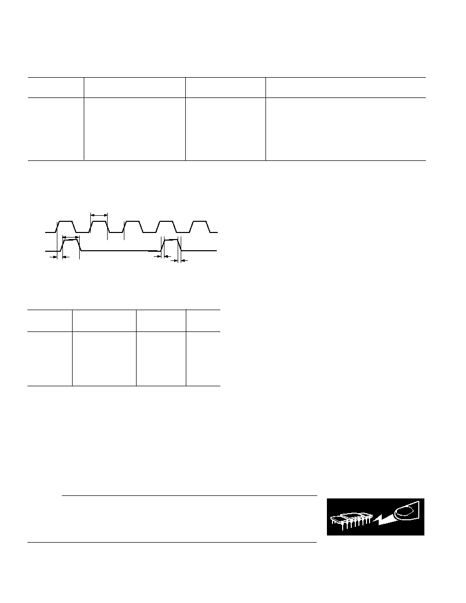
TIMING CHARACTERISTICS
1, 2, 3
Limit at T
MIN
, T
MAX
Parameter
(B and Y Version)
Units
Conditions/Comments
f
CLKIN
6.144
MHz max
t
HIGH
/t
LOW
55/45
max
Input Clock Mark/Space Ratio
45/55
min
t
1
9
ns typ
f
CLOCK
Rising Edge to f
OUT
Rising Edge
t
2
4
ns typ
f
OUT
Rise Time
t
3
4
ns typ
f
OUT
Fall Time
t
4
t
HIGH
±
5
ns typ
f
OUT
Pulsewidth
NOTES
1
Guaranteed by design and characterization, not production tested.
2
All input signals are specified with tr = tf = 5 ns (10% to 90% of V
DD
) and timed from a voltage level of (V
IL
+ V
IH
)/2.
3
See Figure 1.
Specifications subject to change without notice.
(V
DD
= +4.75 V to +5.25 V; V
REF
= +2.5 V. All specifications T
MIN
to T
MAX
unless otherwise noted.)
ABSOLUTE MAXIMUM RATINGS
1, 2
(T
A
= +25
°
C unless otherwise noted)
V
DD
to GND . . . . . . . . . . . . . . . . . . . . . . . . . . 0.3 V to +7 V
Analog Input Voltage to GND . . . . . . . . 5 V to V
DD
+ 0.3 V
Digital Input Voltage to GND . . . . . . . 0.3 V to V
DD
+ 0.3 V
Reference Input Voltage to GND . . . . 0.3 V to V
DD
+ 0.3 V
f
OUT
to GND . . . . . . . . . . . . . . . . . . . . 0.3 V to V
DD
+ 0.3 V
Operating Temperature Range
Automotive (Y Version) . . . . . . . . . . . . . . 40
°
C to +105
°
C
Industrial (B Version) . . . . . . . . . . . . . . . . 40
°
C to +85
°
C
Storage Temperature Range . . . . . . . . . . . . 65
°
C to +150
°
C
Junction Temperature . . . . . . . . . . . . . . . . . . . . . . . . +150
°
C
Plastic DIP Package
Power Dissipation . . . . . . . . . . . . . . . . . . . . . . . . . 450 mW
JA
Thermal Impedance (8 Lead) . . . . . . . . . . . . . 125
°
C/W
JA
Thermal Impedance (16 Lead) . . . . . . . . . . . . 117
°
C/W
Lead Temperature, Soldering
Vapor Phase (60 sec) . . . . . . . . . . . . . . . . . . . . . +215
°
C
Infrared (15 sec) . . . . . . . . . . . . . . . . . . . . . . . . . +220
°
C
SOIC Package
Power Dissipation . . . . . . . . . . . . . . . . . . . . . . . . . 450 mW
JA
Thermal Impedance (8 Lead) . . . . . . . . . . . . . 157
°
C/W
JA
Thermal Impedance (16 Lead) . . . . . . . . . . . . 125
°
C/W
Lead Temperature, Soldering
Vapor Phase (60 sec) . . . . . . . . . . . . . . . . . . . . . +215
°
C
Infrared (15 sec) . . . . . . . . . . . . . . . . . . . . . . . . . +220
°
C
NOTES
1
Stresses above those listed under Absolute Maximum Ratings may cause perma-
nent damage to the device. This is a stress rating only; functional operation of the
device at these or any other conditions above those listed in the operational
sections of this specification is not implied. Exposure to absolute maximum rating
conditions for extended periods may affect device reliability.
2
Transient currents of up to 100 mA will not cause SCR latch-up.
ORDERING GUIDE
Temperature
Package
Package
Models
Ranges
Descriptions
Options
AD7741BN
40
°
C to +85
°
C
Plastic DIP
N-8
AD7741BR
40
°
C to +85
°
C
Small Outline
R-8
AD7741YR
40
°
C to +105
°
C
Small Outline
R-8
AD7742BN
40
°
C to +85
°
C
Plastic DIP
N-16
AD7742BR
40
°
C to +85
°
C
Small Outline
R-16A
AD7742YR
40
°
C to +105
°
C
Small Outline
R-16A
CLKIN
f
OUT
t
HIGH
t
4
t
1
t
2
t
3
Figure 1. Timing Diagram
REV. 0
AD7741/AD7742
5
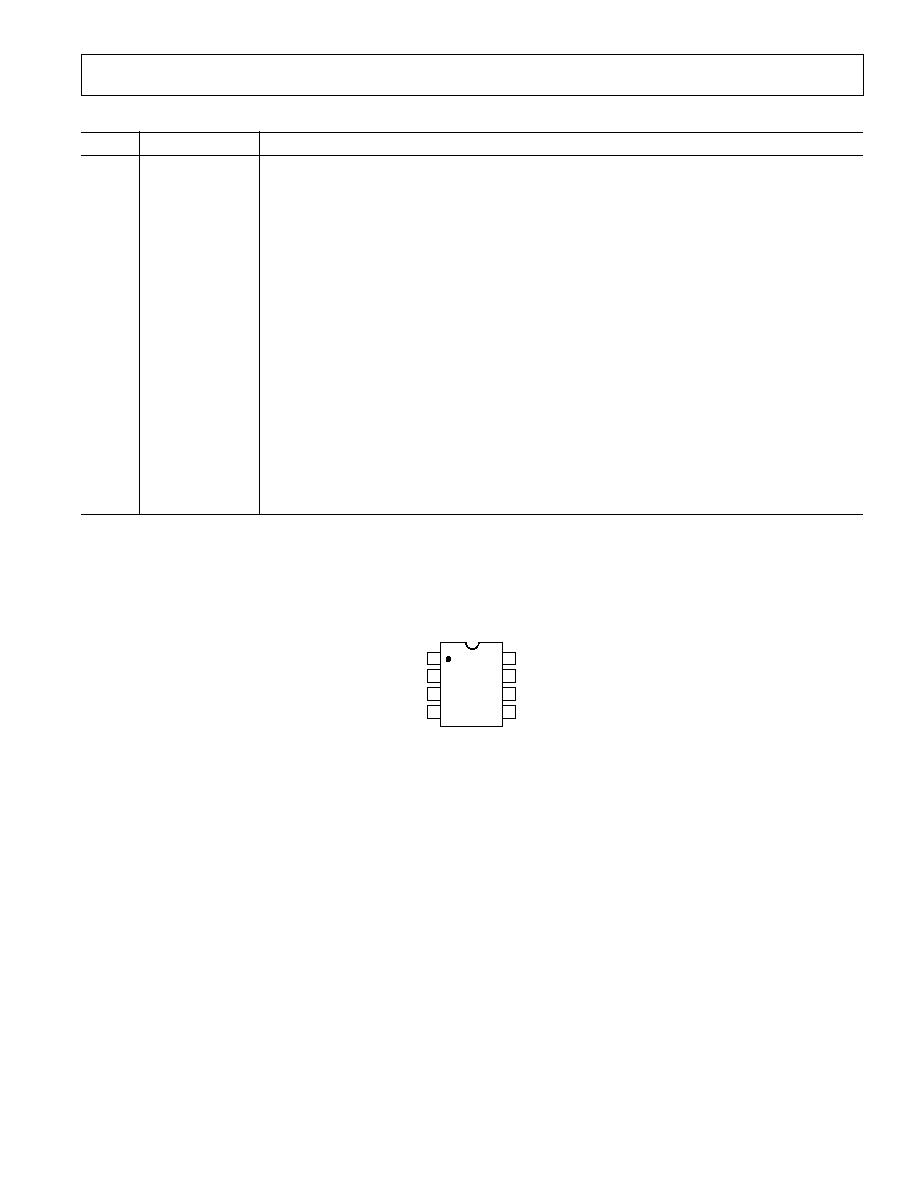
AD7741 PIN FUNCTION DESCRIPTION
Pin No.
Mnemonic
Function
1
V
DD
Power Supply Input. These parts can be operated from +4.75 V to +5.25 V and the supply should
be adequately decoupled to GND.
2
GND
Ground reference point for all circuitry on the part.
3
CLKOUT
External Clock Output. When the master clock for the device is a crystal, the crystal is connected
between CLKIN and CLKOUT. When an external clock is applied to CLKIN, the CLKOUT pin
provides an inverted clock signal. This clock should be buffered if it is to be used as a clock source
elsewhere in the system.
4
CLKIN
External Clock Input. The master clock for the device can be provided in the form of a crystal or an
external clock. A crystal may be tied across the CLKIN and CLKOUT pins. Alternatively, the
CLKIN pin may be driven by a CMOS-compatible clock and CLKOUT left unconnected. The
frequency of the master clock may be as high as 6 MHz.
5
REFIN/OUT
This is the reference input to the core of the VFC and defines the span of the VFC. If this pin is left
unconnected, the internal 2.5 V reference is used. Alternatively, a precision external reference (e.g.,
REF192) may be used to overdrive the internal reference. The internal bandgap reference has a
high output impedance in order to allow it to be overdriven.
6
V
IN
The analog input to the VFC. It has an input range from 0 V to V
REF
. This input is buffered so it
draws virtually no current from whatever source is driving it.
7
PD
Active Low Power-Down pin. When this input is low, the part enters power-down mode where it
typically consumes 15
µ
A of current.
8
f
OUT
Frequency Output. This pin provides the output of the synchronous VFC.
PIN CONFIGURATION
TOP VIEW
(Not to Scale)
8
7
6
5
1
2
3
4
V
DD
f
OUT
AD7741
GND
PD
CLKOUT
V
IN
CLKIN
REFIN/OUT
REV. 0
AD7741/AD7742
6
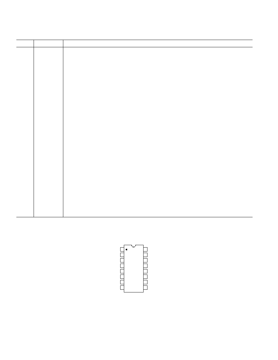
AD7742 PIN FUNCTION DESCRIPTION
Pin No.
Mnemonic
Function
1
f
OUT
Frequency Output. This pin provides the output of the synchronous VFC.
2
V
DD
Power Supply Input. These parts can be operated from +4.75 V to +5.25 V and the supply should be
adequately decoupled to GND.
3
GND
Ground reference point for all circuitry on the part.
45
A1, A0
Address Inputs used to select the input channel configuration.
6
CLKOUT
External Clock Output. When the master clock for the device is a crystal, the crystal is connected be-
tween CLKIN and CLKOUT. When an external clock is applied to CLKIN, the CLKOUT pin
provides an inverted clock signal. This clock should be buffered if it is to be used as a clock source
elsewhere in the system.
7
CLKIN
External Clock Input. The master clock for the device can be provided in the form of a crystal or an
external clock. A crystal may be tied across the CLKIN and CLKOUT pins. Alternatively, the CLKIN
pin may be driven by a CMOS-compatible clock and CLKOUT left unconnected. The frequency of the
master clock may be as high as 6 MHz.
8
UNI/
BIP
Control input which determines whether the device operates with differential bipolar analog input
signals or differential unipolar analog input signals.
9
REFOUT
2.5 V Voltage Reference Output. This can be tied directly to REFIN. It may also be used as a reference
to other parts of the system provided it is buffered first.
10
REFIN
This is the Reference Input to the core of the VFC and defines the span of the VFC. A 2.5 V reference
is required at this pin. This may be provided by connecting it directly to REFOUT or by using a preci-
sion external reference (e.g., REF192).
11
V
IN
1
Buffered Analog Input Channel 1. This is either a pseudo-differential input with respect to V
IN
4 or it is
the positive input of a truly-differential input pair with respect to V
IN
2.
12
V
IN
2
Buffered Analog Input Channel 2. This is either a pseudo-differential input with respect to V
IN
4 or it is
the negative input of a truly-differential input pair with respect to V
IN
1.
13
V
IN
3
Buffered Analog Input Channel 3. This is the positive input of a truly-differential input pair with re-
spect to V
IN
4.
14
V
IN
4
Buffered Analog Input Channel 4. This is either the common for pseudo-differential input with respect
to V
IN
1 or V
IN
2 or it is the negative input of a truly-differential input pair with respect to V
IN
3.
15
GAIN
Gain Select input that controls whether the gain on the analog front-end is X1 or X2.
16
PD
Active Low Power-Down pin. When this input is low, the part enters power-down mode where it typi-
cally consumes 25
µ
A of current.
PIN CONFIGURATION
TOP VIEW
(Not to Scale)
16
15
14
13
12
11
10
9
1
2
3
4
5
6
7
8
f
OUT
PD
AD7742
V
DD
GAIN
GND
V
IN
4
A1
V
IN
3
A0
V
IN
2
CLKOUT
V
IN
1
CLKIN
REFIN
UNI/
BIP
REFOUT
REV. 0
AD7741/AD7742
7
TERMINOLOGY
INTEGRAL NONLINEARITY
For the VFC, Integral Nonlinearity (INL) is a measure of the
maximum deviation from a straight line passing through the
actual endpoints of the VFC transfer function. The error is
expressed in % of the frequency span:
Frequency Span = f
OUT(max)
f
OUT(min)
OFFSET ERROR
This is a measure of the offset error of the VFC. Ideally, the
minimum output frequency (corresponding to minimum input
voltage) is 5% of f
CLKIN
The deviation from this value is the
offset error. It is expressed in terms of the error referred to the
input voltage. It is expressed in mV.
GAIN ERROR
This is a measure of the span error of the VFC. The gain is the
scale factor that relates the input V
IN
to the output f
OUT
. The
gain error is the deviation in slope of the actual VFC transfer
characteristic from the ideal expressed as a percentage of the
full-scale span.
OFFSET ERROR DRIFT
This is a measure of the change in Offset Error with changes in
temperature. It is expressed in
µ
V/
°
C.
GAIN ERROR DRIFT
This is a measure of the change in Gain Error with changes in
temperature. It is expressed in (ppm of span)/
°
C.
POWER-SUPPLY REJECTION RATIO (PSRR)
This indicates how the output of the VFC is affected by changes
in the supply voltage. Again, this error is referred to the input
voltage. The input voltage is kept constant and the V
DD
supply
is varied
±
5%. The ratio of the apparent change in input voltage
to the change in V
DD
is measured in dBs.
CHANNEL-TO-CHANNEL ISOLATION
This is a ratio of the amplitude of the signal at the input of one
channel to a sine wave on the input of another channel. It is
measured in dBs.
COMMON-MODE REJECTION
For the AD7742, the output frequency should remain un-
changed provided the differential input remains unchanged
although its common-mode level may change. The CMR is the
ratio of the apparent change in differential input voltage to the
actual change in common-mode voltage. It is expressed in dBs.
GENERAL DESCRIPTION
The AD7741/AD7742 are a new generation of CMOS synchro-
nous Voltage-to-Frequency Converters (VFCs) that use a
charge-balance conversion technique. The AD7741 is a single-
channel version and the AD7742 is a multichannel version. The
input voltage signal is applied to a proprietary programmable
gain front-end based around an analog modulator that converts
the input voltage into an output pulse train.
The parts also contain an on-chip +2.5 V bandgap reference
and operate from a single +5 V supply. A block diagram of the
AD7742 is shown in Figure 2.
INTEGRATOR
COMPARATOR
SWITCHED
CAPS
SWITCHED
CAPS
f
OUT
INPUT
MUX
V
IN
1
V
IN
2
V
IN
3
V
IN
4
Figure 2. AD7742 Block Diagram
Input Amplifier Stage
The buffered input stage for the analog inputs presents a high
impedance, allowing significant external source impedances.
The four analog inputs (V
IN
1 through V
IN
4) each have a voltage
range from +0.5 V to V
DD
1.75 V. This is an absolute voltage
range and is relative to the GND pin.
In the case of the AD7742 multichannel part, a differential
multiplexer switches one of the differential input channels to the
VFC modulator. The multiplexer is controlled by two pins, A1
and A0. See Table I for channel configurations.
Table I. AD7742 Input Channel Selection
A1
A0
V
IN
(+)
V
IN
()
Type
0
0
V
IN
1
V
IN
4
Pseudo Differential
0
1
V
IN
2
V
IN
4
Pseudo Differential
1
0
V
IN
3
V
IN
4
Full Differential
1
1
V
IN
1
V
IN
2
Full Differential
Analog Input Ranges
The AD7741 has a unipolar single-ended input channel whereas
the AD7742 contains four input channels which may be con-
figured as two fully differential channels or as three pseudo-
differential channels. The AD7742 also has a X1/X2 gain
option on the front end. The channel and gain settings are
pin-programmable.
The AD7742 uses differential inputs to provide common-mode
noise rejection (i.e., the converted result will correspond to the
differential voltage between the two inputs). The absolute voltage
on both inputs must lie between +0.5 V and V
DD
1.75 V.
REV. 0
AD7741/AD7742
8
As can be seen from Table II, the AD7741 has one input range
configuration whereas the AD7742 has unipolar/bipolar as
well as gain options depending on the status of the GAIN
and UNI/
BIP pins.
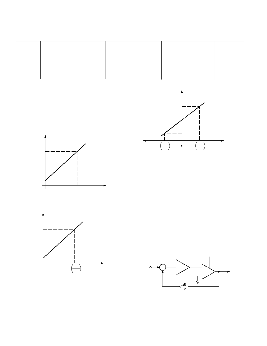
The transfer function for the AD7741 is shown in Figure 3.
Figure 4 shows the AD7742 transfer function for unipolar input
range configuration while the AD7742 transfer function for
bipolar input range configuration is shown in Figure 5.
OUTPUT
FREQUENCY
f
OUT
f
OUT
MAX
(0.45 f
CLKIN
)
f
OUT
MIN
(0.05 f
CLKIN
)
0
INPUT
VOLTAGE V
IN
REFIN
Figure 3. AD7741 Transfer Characteristic for Input Range
from 0 to V
REF
OUTPUT
FREQUENCY
f
OUT
f
OUT
MAX
(0.45 f
CLKIN
)
f
OUT
MIN
(0.05 f
CLKIN
)
0
V
REF
GAIN
+
DIFFERENTIAL
INPUT VOLTAGE
Figure 4. AD7742 Transfer Characteristic for Unipolar
Differential Input Range: 0 V to V
REF
/Gain; the input
common-mode range must be between +0.5 V and
V
DD
1.75 V. UNI/
BIP pin tied to V
DD
.
Table II. AD7741/AD7742 Input Range Selection
V
IN
(Min)
V
IN
(Max)
UNI/
BIP
GAIN
Gain, G
f
OUT
= 0.05 f
CLKIN
f
OUT
= 0.45 f
CLKIN
Part
N/A
N/A
X1
0
+V
REF
AD7741
0
0
X1
V
REF
+V
REF
AD7742
0
1
X2
V
REF
/2
+V
REF
/2
AD7742
1
0
X1
0
+V
REF
AD7742
1
1
X2
0
+V
REF
/2
AD7742
OUTPUT
FREQUENCY
f
OUT
f
OUT
MAX
(0.45 f
CLKIN
)
f
OUT
MIN
(0.05 f
CLKIN
)
DIFFERENTIAL
INPUT VOLTAGE
V
REF
GAIN
+
V
REF
GAIN
Figure 5. AD7742 Transfer Characteristic for Bipolar
Differential Input Range: V
REF
/Gain to +V
REF
/Gain; the
common-mode range must be between +0.5 V and
V
DD
1.75 V. UNI/
BIP pin tied to GND.
VFC Modulator
The analog input signal to the AD7741/AD7742 is continu-
ously sampled by a switched capacitor modulator whose sam-
pling rate is set by a master clock input that may be supplied
externally or by a crystal-controlled on-chip clock oscillator.
However, the input signal is buffered on-chip before being ap-
plied to the sampling capacitor of the modulator. This isolates
the sampling capacitor charging currents from the analog input
pins.
This system is a negative feedback loop that tries to keep the net
charge on the integrator capacitor at zero, by balancing charge
injected by the input voltage with charge injected by the V
REF
.
The output of the comparator provides the digital input for the
1-bit DAC, so that the system functions as a negative feedback
loop that tries to minimize the difference signal (see Figure 6).
INTEGRATOR
COMPARATOR
+
CLK
1-BIT
STREAM
+
INPUT
+V
REF
V
REF
Figure 6. AD7741/AD7742 Modulator Loop
REV. 0
AD7741/AD7742
9
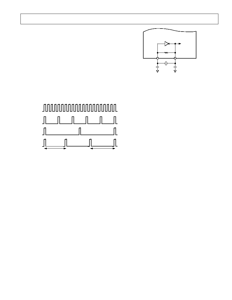
AD7741/AD7742
CLKOUT
CLKIN
C1
C2
TO OTHER
CIRCUITRY
5M
Figure 8. On-Chip Oscillator
The on-chip oscillator circuit also has a start-up time associated
with it before it oscillates at its correct frequency and correct
voltage levels. The typical start-up time for the circuit is 5 ms
(with a 6.144 MHz crystal).
The AD7741/AD7742 master clock appears on the CLKOUT
pin of the device. The maximum recommended load on this pin
is one CMOS load. When using a crystal to generate the AD7741/
AD7742 clock it may be desirable to then use this clock as the
clock source for the system. In this case it is recommended that
the CLKOUT signal be buffered with a CMOS buffer before
being applied to the rest of the circuit.
Reference Input
The AD7741/AD7742 performs conversion relative to an applied
reference voltage that allows easy interfacing to ratiometric
systems. This reference may be applied using the internal 2.5 V
bandgap reference. For the AD7741, this is done by simply
leaving REFIN/OUT unconnected. For the AD7742, REFIN is
tied to REFOUT. Alternatively, an external reference, e.g.,
REF192 or AD780, may be used. For the AD7741, this is con-
nected to REFIN/OUT and will overdrive the internal refer-
ence. For the AD7742, it is connected directly to the REFIN
pin.
While the internal reference will be adequate for most applica-
tions, power supply rejection and overall regulation may be
improved through the use of an external precision reference.
The process of selecting an external voltage reference should
include consideration of drive capability, initial error, noise and
drift characteristics. A suitable choice would be the AD780 or
REF192.
Power-Down Mode
The low power standby mode is initiated by taking the
PD pin
low, which shuts down most of the analog and digital circuitry.
This reduces the power consumption to 185
µ
W max.
The digital data that represents the analog input voltage is con-
tained in the duty cycle of the pulse train appearing at the out-
put of the comparator. The output is a fixed-width pulse whose
frequency depends on the analog input signal. The input voltage
is offset internally so that a full-scale input gives an output fre-
quency of 0.45 f
CLKIN
and zero-scale input gives an output fre-
quency of 0.05 f
CLKIN
. The output allows simple interfacing to
either standard logic families or opto-couplers. The clock high
period controls the pulsewidth of the frequency output. The
pulse is initiated by the edge of the clock signal. The delay time
between the edge of the clock and the edge of the frequency
output is typically 9 ns. Figure 7 shows the waveform of this
frequency output.
After power-up, or if there is a step change in input voltage,
there is a settling time that must elapse before valid data is
obtained. This is typically 2 CLKIN cycles on the AD7742 and
10 CLKIN cycles on the AD7741.
6 T
CLK
7 T
CLK
AVERAGE f
OUT
IS f
CLKIN
*3/20 BUT THE ACTUAL PULSE STREAM
VARIES BETWEEN f
CLKIN
/6 AND f
CLKIN
/7
f
CLKIN
f
OUT
= f
CLKIN
/4
V
IN
= V
REF
/2
f
OUT
= f
CLKIN
/10
V
IN
= V
REF
/8
f
OUT
= f
CLKIN
*3/20
V
IN
= V
REF
/4
Figure 7. AD7741/AD7742 Frequency Output Waveforms
Clock Generation
As distinct from the asynchronous VFCs which rely on the stability
of an external capacitor to set their full-scale frequency, the
AD7741/AD7742 uses an external clock to define the full-scale
output frequency. The result is a more stable, more linear trans-
fer function and also allows the designer to determine the sys-
tem stability and drift based upon the external clock selected. A
crystal oscillator may also be used if desired.
The AD7741/AD7742 requires a master clock input, which may
be an external CMOS-compatible clock signal applied to the
CLKIN pin (CLKOUT not used). Alternatively, a crystal of the
correct frequency can be connected between CLKIN and
CLKOUT, when the clock circuit will function as a crystal
controlled oscillator. Figure 8 shows a simple model of the on-
chip oscillator.
REV. 0
AD7741/AD7742
10
APPLICATIONS
The basic connection diagram for the part is shown in Figure 9.
In the connection diagram shown, the AD7742 analog inputs
are configured as fully differential, bipolar inputs with a gain of
1. A quartz crystal provides the master clock source for the part.
It may be necessary to connect capacitors (C1 and C2 in the
diagram) on the crystal to ensure that it does not oscillate at over-
tones of its fundamental operating frequency. The values of ca-
pacitors will vary depending on the manufacturer's specifications.
CLKOUT
CLKIN
REFIN
f
OUT
GND
UNI/
BIP
GAIN
C1
C2
DIFF
INPUT 1
DIFF
INPUT 2
CHANNEL
SELECT
V
IN
1
V
IN
2
V
IN
3
V
IN
4
A0
A1
V
DD
PD
AD7742
+5V
REFOUT
Figure 9. Basic Connection Diagram
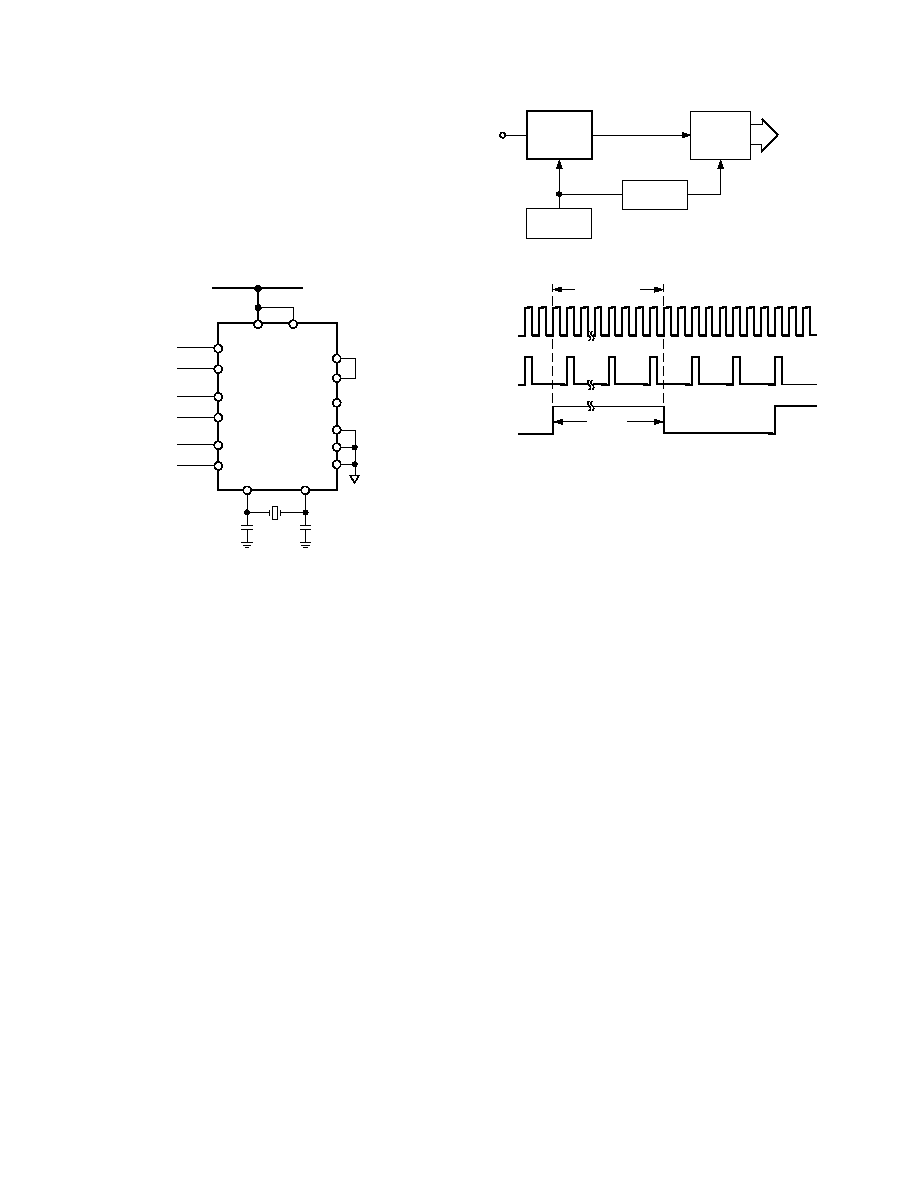
A/D Conversion Techniques Using the AD7741/AD7742
When used as an ADC, VFCs provide certain advantages in-
cluding accuracy, linearity and being inherently monotonic. The
AD7741/AD7742 has a true integrating input which smooths
out noise peaks.
The most popular method of using a VFC in an A/D system is
to count the output pulses of f
OUT
for a fixed gate interval (see
Figure 10). This fixed gate interval should be generated by
dividing down the clock input frequency. This ensures that any
errors due to clock jitter or clock frequency drift are eliminated.
The ratio of the f
OUT
to the clock frequency is what is important
here, not the absolute value of f
OUT
. The frequency division can
be done by a binary counter where f
CLKIN
is the CLK input.
Figure 11 shows the waveforms of f
CLKIN
, f
OUT
and the Gate
signal. A counter counts the rising edges of f
OUT
while the Gate
signal is high. Since the gate interval is not synchronized with
f
OUT
, there is a possibility of a counting inaccuracy. Depending
on f
OUT,
an error of one count may occur.
COUNTER
AD7741
f
OUT
V
IN
CLOCK
GENERATOR
GATE
SIGNAL
TO P
CLKIN
FREQUENCY
DIVIDER
Figure 10. A/D Conversion Using the AD7741 VFC
f
CLKIN
f
OUT
GATE
T
GATE
4096x T
CLOCK
Figure 11. Waveforms in an A/D Converter Using a VFC
The clock frequency and the gate time determine the resolution
of such an ADC. If 12-bit resolution is required and f
CLKIN
is
5 MHz (therefore, f
OUT
max is 2.25 MHz), the minimum gate
time required is calculated as follows:
N counts at Full Scale (2.25 MHz) will take
(N/2.25
×
10
6
) seconds = minimum gate time.
N is the total number of codes for a given resolution; 4096 for
12 bits
minimum gate time = (4096/2.25
×
10
6
) sec = 1.820 ms.
Since T
GATE
×
f
OUT
max = number of counts at full scale, a
faster conversion with the same resolution can be performed
with a higher f
OUT
max. This high f
OUT
max (3 MHz) is a main
feature of the AD7741/AD7742.
If the output frequency is measured by counting pulses gated to
a signal which is derived from the clock, the clock stability is
unimportant and the device simply performs as a voltage-
controlled frequency divider, producing a high resolution ADC.
The inherent monotonicity of the transfer function and wide
range of input clock frequencies allows the conversion time and
resolution to be optimized for specific applications.
There is another parameter is taken into account when choosing
the length of the gate interval. Because the integration period of
the system is equal to the gate interval, any interfering signal can
be rejected by counting for an integer number of periods of the
interfering signal. For example, a gate interval of 100 ms will
give normal-mode rejection of 50 Hz and 60 Hz signals.
REV. 0
AD7741/AD7742
11
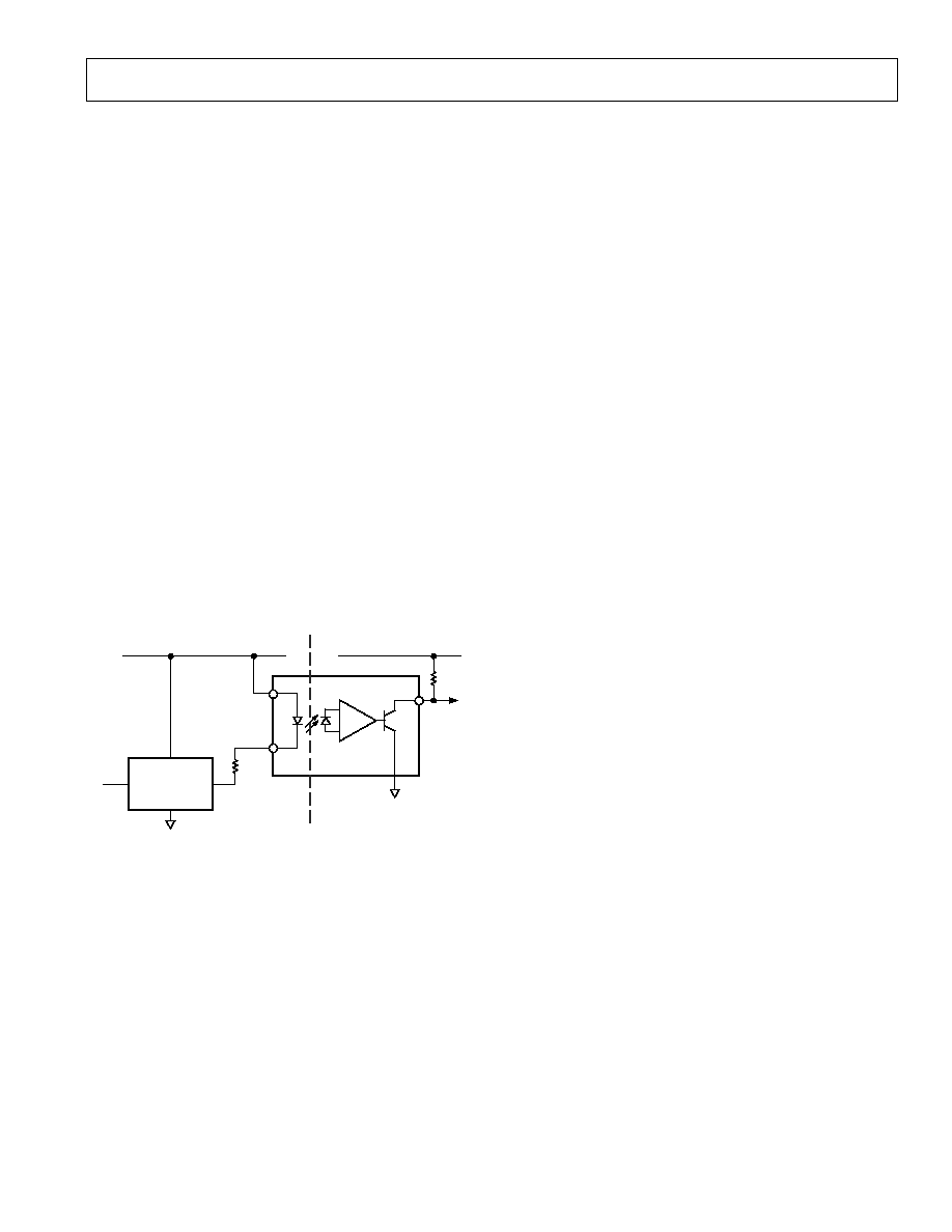
Isolation Applications
In addition to analog-to-digital conversion, the AD7741/AD7742
can be used in isolated analog signal transmission applications.
Due to noise, safety requirements or distance, it may be neces-
sary to isolate the AD7741/AD7742 from any controlling
circuitry. This can easily be achieved by using opto-isolators,
which will provide isolation in excess of 3 kV.
Opto-electronic coupling is a popular method of isolated signal
coupling. In this type of device, the signal is coupled from an
input LED to an output photo-transistor, with light as the con-
necting medium. This technique allows dc to be transmitted, is
extremely useful in overcoming ground loops between equip-
ment, and is applicable over a wide range of speeds and power.
The analog voltage to be transmitted is converted to a pulse
train using the VFC. An opto-isolator circuit is used to couple
this pulse train across an isolation barrier using light as the
connecting medium. The input LED of the isolator is driven
from the output of the AD7741/AD7742. At the receiver side,
the output transistor is operated in the photo-transistor mode.
The pulse train can be reconverted to an analog voltage using a
frequency-to-voltage converter; alternatively, the pulse train can
be fed into a counter to generate a digital signal.
The analog and digital sections of the AD7741/AD7742 have
been designed to allow operation from a single-ended power
source, simplifying its use with isolated power supplies.
Figure 12 shows a general purpose VFC circuit using a low cost
opto-isolator. A +5 V power supply is assumed for both the
isolated (+5 V isolated) and local (+5 V local) supplies.
OPTOCOUPLER
V
CC
R
f
OUT
IN
V
DD
+5V
AD774x
GND1
GND2
ISOLATION
BARRIER
Figure 12. Opto-Isolated Application
Power Supply Bypassing and Grounding
In any circuit where accuracy is important, careful consideration
of the power supply and ground return layout helps to ensure
the rated performance. The printed circuit board housing the
AD7741/AD7742 should be designed so the analog and digital
sections are separated and confined to certain areas of the board.
To minimize capacitive coupling between them, digital and
analog ground planes should only be joined in one place, close
to the DUT and should not overlap.
Avoid running digital lines under the device as these will couple
noise onto the die. The analog ground plane should be allowed
to run under the AD7742 to avoid noise coupling. The power
supply lines to the AD7742 should use as large a trace as pos-
sible to provide low impedance paths and reduce the effects of
glitches on the power supply line. Fast switching signals like
clocks should be shielded with digital ground to avoid radiating
noise to other parts of the board and clock signals should never
be run near analog inputs. Avoid crossover of digital and analog
signals. Traces on opposite sides of the board should run at
right angles to each other. This reduces the effect of feedthrough
through the board. A microstrip technique is by far the best but
is not always possible with a double-sided board. In this tech-
nique, the component side of the board is dedicated to the ground
plane while the signal traces are placed on the solder side.
Good decoupling is also important. All analog supplies should
be decoupled to GND with surface mount capacitors, 10
µ
F in
parallel with 0.1
µ
F located as close to the package as possible,
ideally right up against the device. The lead lengths on the by-
pass capacitor should be as short as possible. It is essential that
these capacitors be placed physically close to the AD7741/AD7742
to minimize the inductance of the PCB trace between the ca-
pacitor and the supply pin. The 10
µ
F are the tantalum bead
type and are located in the vicinity of the VFC to reduce low-
frequency ripple. The 0.1
µ
F capacitors should have low Effec-
tive Series Resistance (ESR) and Effective Series Inductance
(ESI), such as the common ceramic types, which provide a low
impedance path to ground at high frequencies to handle tran-
sient currents due to internal logic switching. Additionally, it is
beneficial to have large capacitors (> 47
µ
F) located at the point
where the power connects to the PCB.
REV. 0
AD7741/AD7742
12
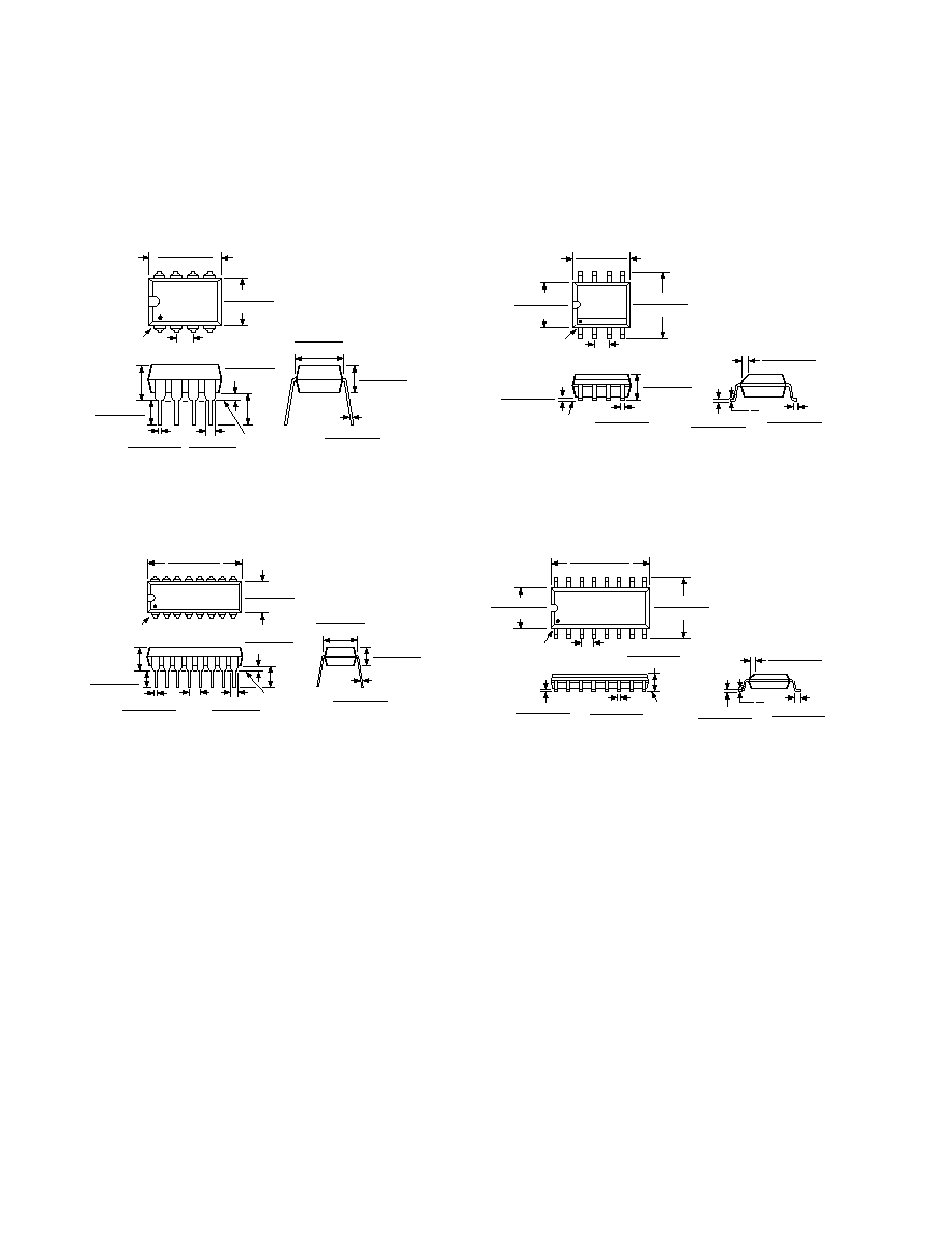
OUTLINE DIMENSIONS
Dimensions shown in inches and (mm).
C360185/99
PRINTED IN U.S.A.
8-Lead Plastic DIP
(N-8)
SEATING
PLANE
0.060 (1.52)
0.015 (0.38)
0.210
(5.33)
MAX
0.022 (0.558)
0.014 (0.356)
0.160 (4.06)
0.115 (2.93)
0.070 (1.77)
0.045 (1.15)
0.130
(3.30)
MIN
8
1
4
5
PIN 1
0.280 (7.11)
0.240 (6.10)
0.100 (2.54)
BSC
0.430 (10.92)
0.348 (8.84)
0.195 (4.95)
0.115 (2.93)
0.015 (0.381)
0.008 (0.204)
0.325 (8.25)
0.300 (7.62)
16-Lead Plastic DIP
(N-16)
16
1
8
9
PIN 1
0.840 (21.34)
0.745 (18.92)
0.280 (7.11)
0.240 (6.10)
SEATING
PLANE
0.060 (1.52)
0.015 (0.38)
0.210 (5.33)
MAX
0.022 (0.558)
0.014 (0.356)
0.160 (4.06)
0.115 (2.93)
0.100
(2.54)
BSC
0.070 (1.77)
0.045 (1.15)
0.130
(3.30)
MIN
0.195 (4.95)
0.115 (2.93)
0.015 (0.381)
0.008 (0.204)
0.325 (8.25)
0.300 (7.62)
8-Lead SO
(R-8)
0.0098 (0.25)
0.0075 (0.19)
0.0500 (1.27)
0.0160 (0.41)
0.0196 (0.50)
0.0099 (0.25)
45
8
0
0.102 (2.59)
0.094 (2.39)
SEATING
PLANE
0.0098 (0.25)
0.0040 (0.10)
0.0192 (0.49)
0.0138 (0.35)
8
5
4
1
0.1968 (5.00)
0.1890 (4.80)
0.2440 (6.20)
0.2284 (5.80)
PIN 1
0.1574 (4.00)
0.1497 (3.80)
0.0500 (1.27)
BSC
16-Lead Narrow Body SO
(R-16A)
16
9
8
1
0.2440 (6.20)
0.2284 (5.80)
0.1574 (4.00)
0.1497 (3.80)
PIN 1
0.3937 (10.00)
0.3859 (9.80)
0.050 (1.27)
BSC
SEATING
PLANE
0.0098 (0.25)
0.0040 (0.10)
0.0192 (0.49)
0.0138 (0.35)
0.0688 (1.75)
0.0532 (1.35)
8
0
0.0196 (0.50)
0.0099 (0.25)
45
0.0500 (1.27)
0.0160 (0.41)
0.0099 (0.25)
0.0075 (0.19)