Äîêóìåíòàöèÿ è îïèñàíèÿ www.docs.chipfind.ru
a
AD7714*
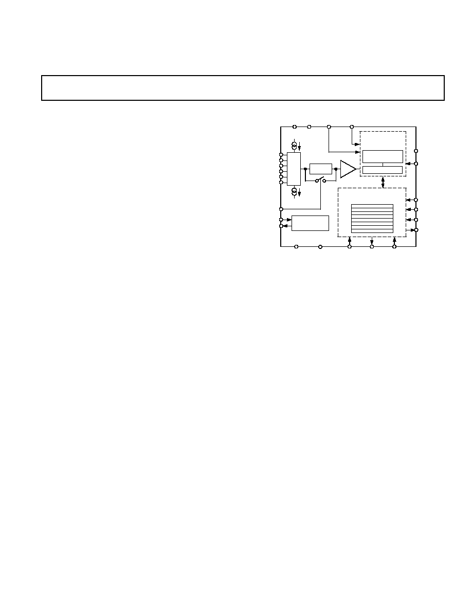
FUNCTIONAL BLOCK DIAGRAM
FEATURES
Charge Balancing ADC
24 Bits No Missing Codes
0.0015% Nonlinearity
Five-Channel Programmable Gain Front End
Gains from 1 to 128
Can Be Configured as Three Fully Differential
Inputs or Five Pseudo-Differential Inputs
Three-Wire Serial Interface
SPITM, QSPITM, MICROWIRETM and DSP Compatible
3 V (AD7714-3) or 5 V (AD7714-5) Operation
Low Noise (<150 nV rms)
Low Current (350
A typ) with Power-Down (5 A typ)
AD7714Y Grade:
+2.7 V to 3.3 V or +4.75 V to +5.25 V Operation
0.0010% Linearity Error
40 C to +105 C Temperature Range
Schmitt Trigger on SCLK and DIN
Low Current (226
A typ) with Power-Down (4 A typ)
Lower Power Dissipation than Standard AD7714
Available in 24-Lead TSSOP Package
Low-Pass Filter with Programmable Filter Cutoffs
Ability to Read/Write Calibration Coefficients
APPLICATIONS
Portable Industrial Instruments
Portable Weigh Scales
Loop-Powered Systems
Pressure Transducers
3 V/5 V, CMOS, 500
A
Signal Conditioning ADC
GENERAL DESCRIPTION
The AD7714 is a complete analog front end for low-frequency
measurement applications. The device accepts low level signals
directly from a transducer and outputs a serial digital word. It
employs a sigma-delta conversion technique to realize up to 24
bits of no missing codes performance. The input signal is applied
to a proprietary programmable gain front end based around an
analog modulator. The modulator output is processed by an on-
chip digital filter. The first notch of this digital filter can be
programmed via the on-chip control register allowing adjust-
ment of the filter cutoff and settling time.
The part features three differential analog inputs (which can also
be configured as five pseudo-differential analog inputs) as well as a
differential reference input. It operates from a single supply (+3 V
or +5 V). The AD7714 thus performs all signal conditioning and
conversion for a system consisting of up to five channels.
The AD7714 is ideal for use in smart, microcontroller- or DSP-
based systems. It features a serial interface that can be configured
REV. C
Information furnished by Analog Devices is believed to be accurate and
reliable. However, no responsibility is assumed by Analog Devices for its
use, nor for any infringements of patents or other rights of third parties
which may result from its use. No license is granted by implication or
otherwise under any patent or patent rights of Analog Devices.
for three-wire operation. Gain settings, signal polarity and channel
selection can be configured in software using the serial port. The
AD7714 provides self-calibration, system calibration and back-
ground calibration options and also allows the user to read and
write the on-chip calibration registers.
CMOS construction ensures very low power dissipation, and the
power-down mode reduces the standby power consumption to
15
µ
W typ. The part is available in a 24-pin, 0.3 inch-wide, plastic
dual-in-line package (DIP); a 24-lead small outline (SOIC)
package, a 28-lead shrink small outline package (SSOP) and a
24-lead thin shrink small outline package (TSSOP).
PRODUCT HIGHLIGHTS
1. The AD7714Y offers the following features in addition to the
standard AD7714: wider temperature range, Schmitt trigger
on SCLK and DIN, operation down to 2.7 V, lower power
consumption, better linearity, and availability in 24-lead
TSSOP package.
2. The AD7714 consumes less than 500
µ
A (f
CLK IN
= 1 MHz)
or 1 mA (f
CLK IN
= 2.5 MHz) in total supply current, making
it ideal for use in loop-powered systems.
3. The programmable gain channels allow the AD7714 to ac-
cept input signals directly from a strain gage or transducer
removing a considerable amount of signal conditioning.
4. The AD7714 is ideal for microcontroller or DSP processor
applications with a three-wire serial interface reducing the num-
ber of interconnect lines and reducing the number of opto-
couplers required in isolated systems. The part contains
on-chip registers that allow control over filter cutoff, input gain,
channel selection, signal polarity and calibration modes.
5. The part features excellent static performance specifications
with 24-bit no missing codes,
±
0.0015% accuracy and low
rms noise (140 nV). Endpoint errors and the effects of tem-
perature drift are eliminated by on-chip self-calibration,
which removes zero-scale and full-scale errors.
*Protected by U.S. Patent No. 5,134,401.
See page 39 for data sheet index.
SPI and QSPI are trademarks of Motorola, Inc.
MICROWIRE is a trademark of National Semiconductor Corporation.
One Technology Way, P.O. Box 9106, Norwood, MA 02062-9106, U.S.A.
Tel: 781/329-4700
World Wide Web Site: http://www.analog.com
Fax: 781/326-8703
© Analog Devices, Inc., 1998
REF IN(+)
MCLK IN
MCLK OUT
A = 1128
CHARGE
BALANCING
A/D CONVERTER
REF IN()
AD7714
BUFFER
AGND
BUFFER
SERIAL INTERFACE
AGND
DGND
REGISTER BANK
-
MODULATOR
SYNC
STANDBY
DIGITAL FILTER
DV
DD
AV
DD
AV
DD
PGA
1 A
1 A
AIN1
AIN2
AIN3
AIN4
AIN5
AIN6
SWITCHING
MATRIX
CLOCK
GENERATION
SCLK
CS
DIN
DOUT
POL
DRDY
RESET
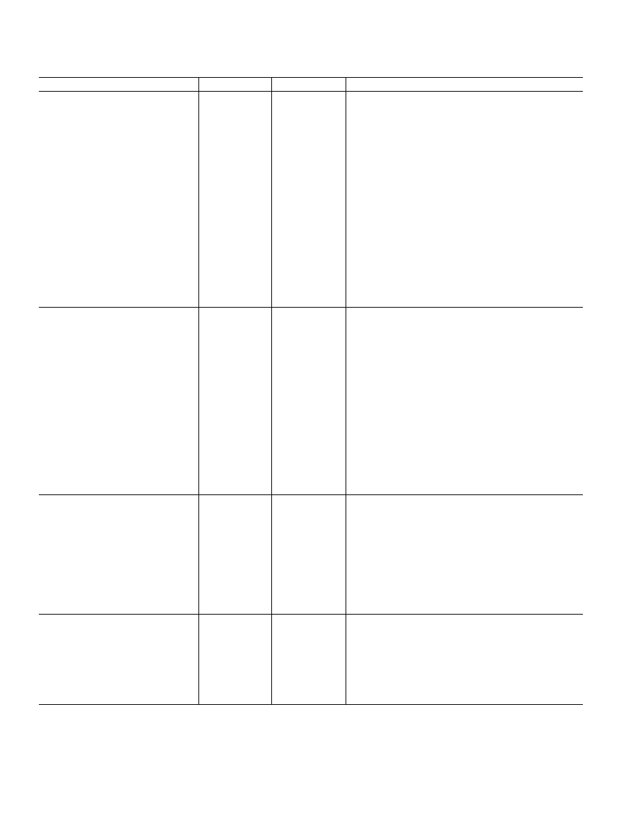
Parameter
A Versions
1
Units
Conditions/Comments
STATIC PERFORMANCE
No Missing Codes
24
Bits min
Guaranteed by Design. Bipolar Mode. For Filter Notches
60 Hz
22
Bits min
For Filter Notch = 100 Hz
18
Bits min
For Filter Notch = 250 Hz
15
Bits min
For Filter Notch = 500 Hz
12
Bits min
For Filter Notch = 1 kHz
Output Noise
See Tables I to IV
Depends on Filter Cutoffs and Selected Gain
Integral Nonlinearity
±
0.0015
% of FSR max
Filter Notches
60 Hz
Unipolar Offset Error
See Note 2
Unipolar Offset Drift
3
0.5
µ
V/
°
C typ
For Gains of 1, 2, 4
0.3
µ
V/
°
C typ
For Gains of 8, 16, 32, 64, 128
Bipolar Zero Error
See Note 2
Bipolar Zero Drift
3
0.5
µ
V/
°
C typ
For Gains of 1, 2, 4
0.3
µ
V/
°
C typ
For Gains of 8, 16, 32, 64, 128
Positive Full-Scale Error
4
See Note 2
Full-Scale Drift
3, 5
0.5
µ
V/
°
C typ
For Gains of 1, 2, 4
0.3
µ
V/
°
C typ
For Gains of 8, 16, 32, 64, 128
Gain Error
6
See Note 2
Gain Drift
3, 7
0.5
ppm of FSR/
°
C typ
Bipolar Negative Full-Scale Error
±
0.0015
% of FSR max
Typically
±
0.0004%
Bipolar Negative Full-Scale Drift
3
1
µ
V/
°
C typ
For Gains of 1, 2, 4
0.6
µ
V/
°
C typ
For Gains of 8, 16, 32, 64, 128
ANALOG INPUTS/REFERENCE INPUTS
Specifications for AIN and REF IN Unless Noted
Input Common-Mode Rejection (CMR)
90
dB min
At DC. Typically 102 dB
Normal-Mode 50 Hz Rejection
8
100
dB min
For Filter Notches of 10
Hz
, 25
Hz
, 50 Hz,
±
0.02
×
f
NOTCH
Normal-Mode 60 Hz Rejection
8
100
dB min
For Filter Notches of 10
Hz
, 30
Hz
, 60 Hz,
±
0.02
×
f
NOTCH
Common-Mode 50 Hz Rejection
8
150
dB min
For Filter Notches of 10
Hz
, 25
Hz
, 50 Hz,
±
0.02
×
f
NOTCH
Common-Mode 60 Hz Rejection
8
150
dB min
For Filter Notches of 10
Hz
, 30
Hz
, 60 Hz,
±
0.02
×
f
NOTCH
Common-Mode Voltage Range
9
AGND to AV
DD
V min to V max
AIN for BUFFER = 0 and REF IN
Absolute AIN/REF IN Voltage
9
AGND 30 mV
V min
AIN for BUFFER = 0 and REF IN
AV
DD
+ 30 mV
V max
Absolute/Common-Mode AIN Voltage
9
AGND + 50 mV
V min
BUFFER = 1. A Version
AV
DD
1.5 V
V max
AIN Input Current
8
1
nA max
A Version
AIN Sampling Capacitance
8
7
pF max
AIN Differential Voltage Range
10
0 to +V
REF
/GAIN
11
nom
Unipolar Input Range (B/U Bit of Filter High Register = 1)
±
V
REF
/GAIN
nom
Bipolar Input Range (B/U Bit of Filter High Register = 0)
AIN Input Sampling Rate, f
S
GAIN
×
f
CLK IN
/64
For Gains of 1, 2, 4
f
CLK IN
/8
For Gains of 8, 16, 32, 64, 128
REF IN(+) REF IN() Voltage
+2.5
V nom
±
1% for Specified Performance. Functional with Lower V
REF
REF IN Input Sampling Rate, f
S
f
CLK IN
/64
LOGIC INPUTS
Input Current
±
10
µ
A max
All Inputs Except MCLK IN
V
INL
, Input Low Voltage
0.8
V max
DV
DD
= +5 V
V
INL
, Input Low Voltage
0.4
V max
DV
DD
= +3.3 V
V
INH
, Input High Voltage
2.4
V min
DV
DD
= +5 V
V
INH
, Input High Voltage
2.0
V min
DV
DD
= +3.3 V
MCLK IN Only
V
INL
, Input Low Voltage
0.8
V max
DV
DD
= +5 V
V
INL
, Input Low Voltage
0.4
V max
DV
DD
= +3.3 V
V
INH
, Input High Voltage
3.5
V min
DV
DD
= +5 V
V
INH
, Input High Voltage
2.5
V min
DV
DD
= +3.3 V
LOGIC OUTPUTS (Including MCLK OUT)
V
OL
, Output Low Voltage
0.4
V max
I
SINK
= 800
µ
A Except for MCLK OUT.
12
DV
DD
= +5 V
V
OL
, Output Low Voltage
0.4
V max
I
SINK
= 100
µ
A Except for MCLK OUT.
12
DV
DD
= +3.3 V
V
OH
, Output High Voltage
4.0
V min
I
SOURCE
= 200
µ
A Except for MCLK OUT.
12
DV
DD
= +5 V
V
OH
, Output High Voltage
DV
DD
0.6 V
V min
I
SOURCE
= 100
µ
A Except for MCLK OUT.
12
DV
DD
= +3.3 V
Floating State Leakage Current
±
10
µ
A max
Floating State Output Capacitance
13
9
pF typ
Data Output Coding
Binary
Unipolar Mode
Offset Binary
Bipolar Mode
NOTES
1
Temperature range is as follows: A Versions: 40
°
C to +85
°
C.
2
A calibration is effectively a conversion so these errors will be of the order of the conversion noise shown in Tables I to IV. This applies after calibration at the temperature of interest.
3
Recalibration at any temperature will remove these drift errors.
4
Positive Full-Scale Error includes Zero-Scale Errors (Unipolar Offset Error or Bipolar Zero Error) and applies to both unipolar and bipolar input ranges.
5
Full-Scale Drift includes Zero-Scale Drift (Unipolar Offset Drift or Bipolar Zero Drift) and applies to both unipolar and bipolar input ranges.
6
Gain Error does not include Zero-Scale Errors. It is calculated as Full-Scale Error--Unipolar Offset Error for unipolar ranges and Full-Scale Error--Bipolar Zero Error for
bipolar ranges.
AD7714-5SPECIFICATIONS
(AV
DD
= +5 V, DV
DD
= +3.3 V or +5 V, REF IN(+) = +2.5 V; REF IN() = AGND;
f
CLK IN
= 2.4576 MHz unless otherwise noted. All specifications T
MIN
to T
MAX
unless otherwise noted.)
REV. C
2
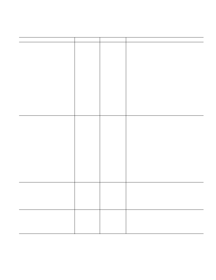
Parameter
A Versions
Units
Conditions/Comments
STATIC PERFORMANCE
No Missing Codes
24
Bits min
Guaranteed by Design. Bipolar Mode. For Filter Notches
60 Hz
22
Bits min
For Filter Notch = 100 Hz
18
Bits min
For Filter Notch = 250 Hz
15
Bits min
For Filter Notch = 500 Hz
12
Bits min
For Filter Notch = 1 kHz
Output Noise
See Tables I to IV
Depends on Filter Cutoffs and Selected Gain
Integral Nonlinearity
±
0.0015
% of FSR max
Filter Notches
60 Hz
Unipolar Offset Error
See Note 2
Unipolar Offset Drift
3
0.4
µ
V/
°
C typ
For Gains of 1, 2, 4
0.1
µ
V/
°
C typ
For Gains of 8, 16, 32, 64, 128
Bipolar Zero Error
See Note 2
Bipolar Zero Drift
3
0.4
µ
V/
°
C typ
For Gains of 1, 2, 4
0.1
µ
V/
°
C typ
For Gains of 8, 16, 32, 64, 128
Positive Full-Scale Error
4
See Note 2
Full-Scale Drift
3, 5
0.4
µ
V/
°
C typ
For Gains of 1, 2, 4
0.1
µ
V/
°
C typ
For Gains of 8, 16, 32, 64, 128
Gain Error
6
See Note 2
Gain Drift
3, 7
0.2
ppm of FSR/
°
C typ
Bipolar Negative Full-Scale Error
±
0.003
% of FSR max
Typically
±
0.0004%
Bipolar Negative Full-Scale Drift
3
1
µ
V/
°
C typ
For Gains of 1, 2, 4
0.6
µ
V/
°
C typ
For Gains of 8, 16, 32, 64, 128
ANALOG INPUTS/REFERENCE INPUTS
Specifications for AIN and REF IN Unless Noted
Input Common-Mode Rejection (CMR)
90
dB min
At DC. Typically 102 dB.
Normal-Mode 50 Hz Rejection
8
100
dB min
For Filter Notches of 10 Hz, 25 Hz, 50 Hz,
±
0.02
×
f
NOTCH
Normal-Mode 60 Hz Rejection
8
100
dB min
For Filter Notches of 10 Hz, 30 Hz, 60 Hz,
±
0.02
×
f
NOTCH
Common-Mode 50 Hz Rejection
8
150
dB min
For Filter Notches of 10 Hz, 25 Hz, 50 Hz,
±
0.02
×
f
NOTCH
Common-Mode 60 Hz Rejection
8
150
dB min
For Filter Notches of 10 Hz, 30 Hz, 60 Hz,
±
0.02
×
f
NOTCH
Common-Mode Voltage Range
9
AGND to AV
DD
V min to V max
AIN for BUFFER = 0 and REF IN
Absolute AIN/REF IN Voltage
9
AGND 30 mV
V min
AIN for BUFFER = 0 and REF IN
AV
DD
+ 30 mV
V max
Absolute/Common-Mode AIN Voltage
9
AGND + 50 mV
V min
BUFFER = 1
AV
DD
1.5 V
V max
AIN Input Current
8
1
nA max
AIN Sampling Capacitance
8
7
pF max
AIN Differential Voltage Range
10
0 to +V
REF
/GAIN
11
nom
Unipolar Input Range (B/U Bit of Filter High Register = 1)
±
V
REF
/GAIN
nom
Bipolar Input Range (B/U Bit of Filter High Register = 0)
AIN Input Sampling Rate, f
S
GAIN
×
f
CLK IN
/64
For Gains of 1, 2, 4
f
CLK IN
/8
For Gains of 8, 16, 32, 64, 128
REF IN(+) REF IN() Voltage
+1.25
V nom
±
1% for Specified Performance. Part Functions with
Lower V
REF
REF IN Input Sampling Rate, f
S
f
CLK IN
/64
LOGIC INPUTS
Input Current
±
10
µ
A max
All Inputs Except MCLK IN
V
INL
, Input Low Voltage
0.4
V max
V
INH
, Input High Voltage
2.0
V min
MCLK IN Only
V
INL
, Input Low Voltage
0.4
V max
V
INH
, Input High Voltage
2.5
V min
LOGIC OUTPUTS (Including MCLK OUT)
V
OL
, Output Low Voltage
0.4
V max
I
SINK
= 100
µ
A Except for MCLK OUT
12
V
OH
, Output High Voltage
DV
DD
0.6
V min
I
SOURCE
= 100
µ
A Except for MCLK OUT
12
Floating State Leakage Current
±
10
µ
A max
Floating State Output Capacitance
13
9
pF typ
Data Output Coding
Binary
Unipolar Mode
Offset Binary
Bipolar Mode
NOTES
7
Gain Error Drift does not include Unipolar Offset Drift/Bipolar Zero Drift. It is effectively the drift of the part if zero-scale calibrations only were performed as is the case with
background calibration.
8
These numbers are guaranteed by design and/or characterization.
9
The common-mode voltage range on the input pairs applies provided the absolute input voltage specification is obeyed.
10
The input voltage range on the analog inputs is given here with respect to the voltage on the respective negative input of its differential or pseudo-differential pair. See Table VII
for which inputs form differential pairs.
11
V
REF
= REF IN(+) REF IN().
12
These logic output levels apply to the MCLK OUT output only when it is loaded with a single CMOS load.
13
Sample tested at +25
°
C to ensure compliance.
14
See Burnout Current section.
AD7714-3SPECIFICATIONS
(AV
DD
= +3.3 V, DV
DD
= +3.3 V, REF IN(+) = +1.25 V; REF IN() = AGND;
f
CLK IN
= 2.4576 MHz unless otherwise noted. All specifications T
MIN
to T
MAX
unless otherwise noted.)
AD7714
REV. C
3
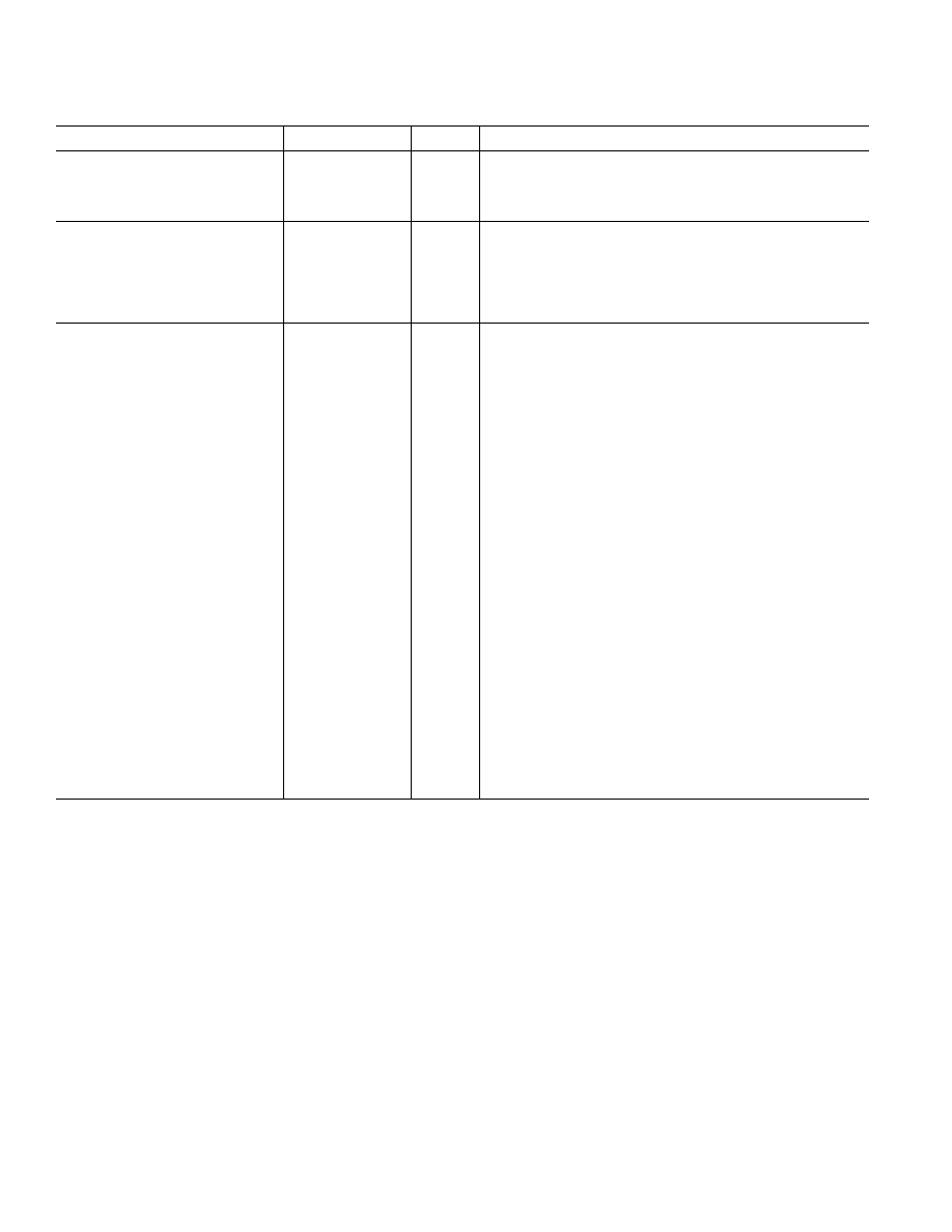
AD7714SPECIFICATIONS
Parameter
A Versions
Units
Conditions/Comments
TRANSDUCER BURNOUT
14
Current
1
µ
A nom
Initial Tolerance
±
10
% typ
Drift
0.1
%/
°
C typ
SYSTEM CALIBRATION
Positive Full-Scale Calibration Limit
15
(1.05
×
V
REF
)/GAIN
V max
GAIN Is the Selected PGA Gain (Between 1 and 128)
Negative Full-Scale Calibration Limit
15
(1.05
×
V
REF
)/GAIN
V max
GAIN Is the Selected PGA Gain (Between 1 and 128)
Offset Calibration Limit
16
(1.05
×
V
REF
)/GAIN
V max
GAIN Is the Selected PGA Gain (Between 1 and 128)
Input Span
16
0.8
×
V
REF
/GAIN
V min
GAIN Is the Selected PGA Gain (Between 1 and 128)
(2.1
×
V
REF
)/GAIN
V max
GAIN Is the Selected PGA Gain (Between 1 and 128)
POWER REQUIREMENTS
Power Supply Voltages
AV
DD
Voltage (AD7714-3)
+3 to +3.6
V
For Specified Performance
AV
DD
Voltage (AD7714-5)
+4.75 to +5.25
V
For Specified Performance
DV
DD
Voltage
+3 to +5.25
V
For Specified Performance
Power Supply Currents
AV
DD
Current
AV
DD
= 3.3 V or 5 V. BST Bit of Filter High Register = 0
17
0.27
mA max
Typically 0.2 mA. BUFFER = 0 V. f
CLK IN
= 1 MHz or 2.4576 MHz
0.6
mA max
Typically 0.4 mA. BUFFER = DV
DD
. f
CLK IN
= 1 MHz or 2.4576 MHz
AV
DD
= 3.3 V or 5 V. BST Bit of Filter High Register = 1
17
0.5
mA max
Typically 0.3 mA. BUFFER = 0 V. f
CLK IN
= 2.4576 MHz
1.1
mA max
Typically 0.8 mA. BUFFER = DV
DD
. f
CLK IN
= 2.4576 MHz
DV
DD
Current
18
Digital I/Ps = 0 V or DV
DD.
External MCLK IN
0.23
mA max
Typically 0.15 mA. DV
DD
= 3.3 V. f
CLK IN
= 1 MHz
0.4
mA max
Typically 0.3 mA. DV
DD
= 5 V. f
CLK IN
= 1 MHz
0.5
mA max
Typically 0.4 mA. DV
DD
= 3.3 V. f
CLK IN
= 2.4576 MHz
0.8
mA max
Typically 0.6 mA. DV
DD
= 5 V. f
CLK IN
= 2.4576 MHz
Power Supply Rejection
19
See Note 20
dB typ
Normal-Mode Power Dissipation
18
AV
DD
= DV
DD
= +3.3 V. Digital I/Ps = 0 V or DV
DD
. External MCLK IN
1.65
mW max
Typically 1.25 mW. BUFFER = 0 V. f
CLK IN
= 1 MHz. BST Bit = 0
2.75
mW max
Typically 1.8 mW. BUFFER = +3.3 V. f
CLK IN
= 1 MHz. BST Bit = 0
2.55
mW max
Typically 2 mW. BUFFER = 0 V. f
CLK IN
= 2.4576 MHz. BST Bit = 0
3.65
mW max
Typically 2.6 mW. BUFFER = +3.3 V. f
CLK IN
= 2.4576 MHz. BST Bit = 0
Normal-Mode Power Dissipation
AV
DD
= DV
DD
= +5 V. Digital I/Ps = 0 V or DV
DD
. External MCLK IN
3.35
mW max
Typically 2.5 mW. BUFFER = 0 V. f
CLK IN
= 1 MHz. BST Bit = 0
5
mW max
Typically 3.5 mW. BUFFER = +5 V. f
CLK IN
= 1 MHz. BST Bit = 0
5.35
mW max
Typically 4 mW. BUFFER = 0 V. f
CLK IN
= 2.4576 MHz. BST Bit = 0
7
mW max
Typically 5 mW. BUFFER = +5 V. f
CLK IN
= 2.4576 MHz. BST Bit = 0
Standby (Power-Down) Current
21
40
µ
A max
External MCLK IN = 0 V or DV
DD
. Typically 20
µ
A. V
DD
= +5 V
Standby (Power-Down) Current
21
10
µ
A max
External MCLK IN = 0 V or DV
DD
. Typically 5
µ
A. V
DD
= +3.3 V
NOTES
15
After calibration, if the input voltage exceeds positive full scale, the converter will output all 1s. If the input is less than negative full scale, then the device outputs all 0s.
16
These calibration and span limits apply provided the absolute voltage on the analog inputs does not exceed AV
DD
+ 30 mV or go more negative than AGND 30 mV. The
offset calibration limit applies to both the unipolar zero point and the bipolar zero point.
17
For higher gains (
8) at f
CLK IN
= 2.4576 MHz, the BST bit of the Filter High Register must be set to 1. For other conditions, it can be set to 0.
18
When using a crystal or ceramic resonator across the MCLK pins as the clock source for the device, the DV
DD
current and power dissipation will vary depending on the crystal
or resonator type (see Clocking and Oscillator Circuit section).
19
Measured at dc and applies in the selected passband. PSRR at 50 Hz will exceed 120 dB with filter notches of 5 Hz, 10 Hz, 25 Hz or 50 Hz. PSRR at 60 Hz will exceed 120 dB
with filter notches of 6 Hz, 10 Hz, 30 Hz or 60 Hz.
20
PSRR depends on gain. For Gain of 1 : 70 dB typ: For Gain of 2 : 75 dB typ; For Gain of 4 : 80 dB typ; For Gains of 8 to 128 : 85 dB typ.
21
If the external master clock continues to run in standby mode, the standby current increases to 150
µ
A typical with 5 V supplies and 75
µ
A typical with 3.3 V supplies. When
using a crystal or ceramic resonator across the MCLK pins as the clock source for the device, the internal oscillator continues to run in standby mode and the power dissipation
depends on the crystal or resonator type (see Standby Mode section).
Specifications subject to change without notice.
(AV
DD
= + 3.3 V to +5 V, DV
DD
= +3.3 V to +5 V, REF IN(+) = +1.25 V (AD7714-3) or +2.5 V
(AD7714-5); REF IN() = AGND; MCLK IN = 1 MHz to 2.4576 MHz unless otherwise noted. All specifications T
MIN
to T
MAX
unless otherwise noted.)
REV. C
4
Parameter
Y Versions
1
Units
Conditions/Comments
STATIC PERFORMANCE
No Missing Codes
24
Bits min
Guaranteed by Design. For Filter Notches
60 Hz
22
Bits min
For Filter Notch = 100 Hz
18
Bits min
For Filter Notch = 250 Hz
15
Bits min
For Filter Notch = 500 Hz
12
Bits min
For Filter Notch = 1 kHz
Output Noise
See Tables I to IV
Depends on Filter Cutoffs and Selected Gain
Integral Nonlinearity
±
0.001
% of FSR max
Filter Notches
60 Hz.
Unipolar Offset Error
See Note 2
Unipolar Offset Drift
3
0.4
µ
V/
°
C typ
For Gains of 1, 2, 4
0.1
µ
V/
°
C typ
For Gains of 8, 16, 32, 64, 128
Bipolar Zero Error
See Note 2
Bipolar Zero Drift
3
0.4
µ
V/
°
C typ
For Gains of 1, 2, 4
0.1
µ
V/
°
C typ
For Gains of 8, 16, 32, 64, 128
Positive Full-Scale Error
4
See Note 2
Full-Scale Drift
3, 5
0.4
µ
V/
°
C typ
For Gains of 1, 2, 4
0.1
µ
V/
°
C typ
For Gains of 8, 16, 32, 64, 128
Gain Error
6
See Note 2
Gain Drift
3, 7
0.2
ppm of FSR/
°
C typ
Bipolar Negative Full-Scale Error
2
±
0.0015
% of FSR max
AV
DD
= 5 V. Typically
±
0.0004%
±
0.003
% of FSR max
AV
DD
= 3 V. Typically
±
0.0004%
Bipolar Negative Full-Scale Drift
3
1
µ
V/
°
C typ
For Gains of 1 to 4
0.6
µ
V/
°
C typ
For Gains of 8 to 128
ANALOG INPUTS/REFERENCE INPUTS
Specifications for AIN and REF IN Unless Noted
Input Common-Mode Rejection (CMR)
8
90
dB min
At DC. Typically 102 dB.
Normal-Mode 50 Hz Rejection
8
100
dB min
For Filter Notches of 10 Hz, 25 Hz, 50 Hz,
±
0.02
×
f
NOTCH
Normal-Mode 60 Hz Rejection
8
100
dB min
For Filter Notches of 10 Hz, 30 Hz, 60 Hz,
±
0.02
×
f
NOTCH
Common-Mode 50 Hz Rejection
8
150
dB min
For Filter Notches of 10 Hz, 25 Hz, 50 Hz,
±
0.02
×
f
NOTCH
Common-Mode 60 Hz Rejection
8
150
dB min
For Filter Notches of 10 Hz, 30 Hz, 60 Hz,
±
0.02
×
f
NOTCH
Absolute/Common-Mode REF IN Voltage
8
AGND to AV
DD
V min to V max
Absolute/Common-Mode AIN Voltage
8,
9
AGND 30 mV
V min
BUF Bit of Setup Register = 0
AV
DD
+ 30 mV
V max
Absolute/Common-Mode AIN Voltage
8, 9
AGND + 50 mV
V min
BUF Bit of Setup Register = 1
AV
DD
1.5 V
V max
AIN DC Input Current
8
1
nA max
AIN Sampling Capacitance
8
7
pF max
AIN Differential Voltage Range
10
0 to +V
REF
/GAIN
11
nom
Unipolar Input Range (B/U Bit of Filter High Register = 1)
±
V
REF
/GAIN
nom
Bipolar Input Range (B/U Bit of Filter High Register = 0)
AIN Input Sampling Rate, f
S
GAIN
×
f
CLK IN
/64
For Gains of 1 to 4
f
CLK IN
/8
For Gains of 8 to 128
Reference Input Range
REF IN(+) REF IN() Voltage
1/1.75
V min/max
AV
DD
= 2.7 V to 3.3 V. V
REF
= 1.25
±
1% for Specified Performance
REF IN(+) REF IN() Voltage
1/3.5
V min/max
AV
DD
= 4.75 V to 5.25 V. V
REF
= 2.5
±
1% for Specified Performance
REF IN Input Sampling Rate, f
S
f
CLK IN
/64
LOGIC INPUTS
Input Current
±
10
µ
A max
All Inputs Except MCLK IN
V
INL
, Input Low Voltage
0.8
V max
DV
DD
= 5 V
0.4
V max
DV
DD
= 3 V
V
INH
, Input High Voltage
2.4
V min
DV
DD
= 5 V
2
V min
DV
DD
= 3 V
SCLK & DIN Only (Schmitt Triggered Input)
DV
DD
= 5 V NOMINAL
V
T+
1.4/3
V min/V max
V
T
0.8/1.4
V min/V max
V
T+
V
T
0.4/0.8
V min/V max
SCLK & DIN Only (Schmitt Triggered Input)
DV
DD
= 3 V NOMINAL
V
T+
1/2.5
V min/V max
V
T
0.4/1.1
V min/V max
V
T+
V
T
0.375/0.8
V min/V max
MCLK In Only
DV
DD
= 5 V NOMINAL
V
INL
, Input Low Voltage
0.8
V max
V
INH
, Input High Voltage
3.5
V min
MCLK In Only
DV
DD
= 3 V NOMINAL
V
INL
, Input Low Voltage
0.4
V max
V
INH
, Input High Voltage
2.5
V min
LOGIC OUTPUTS (Including MCLK OUT)
V
OL
, Output Low Voltage
0.4
V max
I
SINK
= 800
µ
A with DV
DD
= 5 V. Except for MCLK OUT
12
V
OL
, Output Low Voltage
0.4
V max
I
SINK
= 100
µ
A with DV
DD
= 3 V. Except for MCLK OUT
12
V
OH
, Output High Voltage
4
V min
I
SOURCE
= 200
µ
A with DV
DD
= 5 V. Except for MCLK OUT
12
AD7714YSPECIFICATIONS
(AV
DD
= DV
DD
= +2.7 V to +3.3 V or 4.75 V to 5.25 V, REF IN(+) = +1.25 V; with AV
DD
= 3 V
and +2.5 V with AV
DD
= 5 V; REF IN() = AGND; MCLK IN = 2.4576 MHz unless otherwise noted. All specifications T
MIN
to T
MAX
unless otherwise noted.)
AD7714
REV. C
5