Äîêóìåíòàöèÿ è îïèñàíèÿ www.docs.chipfind.ru
a
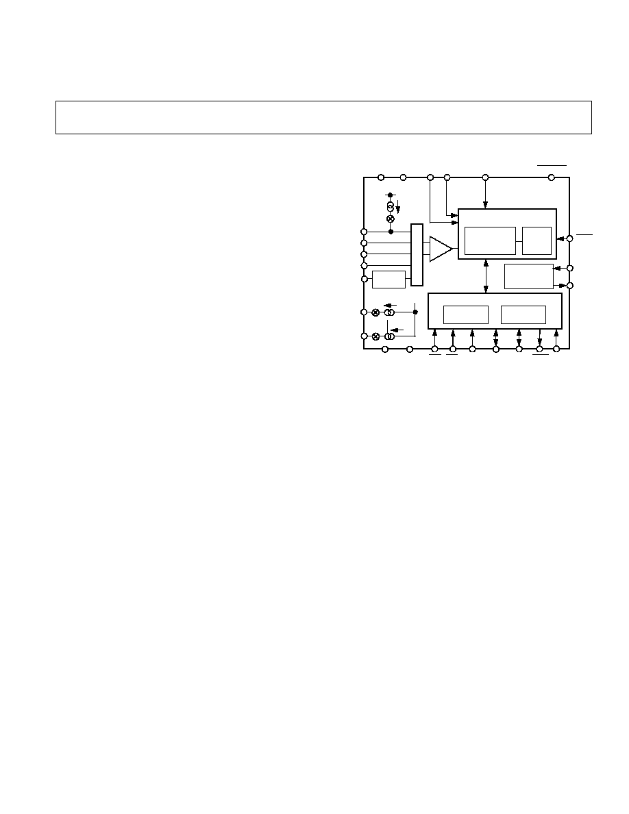
FUNCTIONAL BLOCK DIAGRAM
AD7713
AIN2(+)
AIN2()
AIN3
STANDBY
CLOCK
GENERATION
SERIAL INTERFACE
CONTROL
REGISTER
OUTPUT
REGISTER
CHARGING BALANCING A/D
CONVERTER
AUTO-ZEROED
-
MODULATOR
DIGITAL
FILTER
AGND
DGND
MODE SDATA SCLK
A0
MCLK
OUT
MCLK
IN
AIN1(+)
AIN1()
REF
IN()
REF
IN(+)
AV
DD
DV
DD
AV
DD
1µA
A = 1 128
AV
DD
200µA
V
BIAS
SYNC
DRDY
TFS
RFS
RTD2
PGA
200µA
RTD1
INPUT
SCALING
M
U
X
FEATURES
Charge Balancing ADC
24 Bits No Missing Codes
0.0015% Nonlinearity
Three-Channel Programmable Gain Front End
Gains from 1 to 128
Two Differential Inputs
One Single Ended High Voltage Input
Low-Pass Filter with Programmable Filter Cutoffs
Ability to Read/Write Calibration Coefficients
Bidirectional Microcontroller Serial Interface
Single Supply Operation
Low Power (3.5 mW typ) with Power-Down Mode
(150 W typ)
APPLICATIONS
Loop Powered (Smart) Transmitters
RTD Transducers
Process Control
Portable Industrial Instruments
LC
2
MOS
Loop-Powered Signal Conditioning ADC
REV. C
Information furnished by Analog Devices is believed to be accurate and
reliable. However, no responsibility is assumed by Analog Devices for its
use, nor for any infringements of patents or other rights of third parties
which may result from its use. No license is granted by implication or
otherwise under any patent or patent rights of Analog Devices.
AD7713*
© Analog Devices, Inc., 1995
One Technology Way, P.O. Box 9106, Norwood. MA 02062-9106, U.S.A.
Tel: 617/329-4700
Fax: 617/326-8703
CMOS construction ensures low power dissipation and a hard-
ware programmable power-down mode reduces the standby
power consumption to only 150
µ
W typical. The part is avail-
able in a 24-pin, 0.3 inch wide, plastic and hermetic dual-in-line
package (DIP) as well as a 24-lead small outline (SOIC) package.
PRODUCT HIGHLIGHTS
1. The AD7713 consumes less than 1 mA in total supply cur-
rent, making it ideal for use in loop-powered systems.
2. The two programmable gain channels allow the AD7713 to
accept input signals directly from a transducer removing a
considerable amount of signal conditioning. To maximize the
flexibility of the part, the high level analog input accepts
4
×
V
REF
signals. On-chip current sources provide excitation
for three-wire and four-wire RTD configurations.
3. No Missing Codes ensures true, usable, 24-bit dynamic
range coupled with excellent
±
0.0015% accuracy. The effects
of temperature drift are eliminated by on-chip self-calibration,
which removes zero-scale and full-scale errors.
4. The AD7713 is ideal for microcontroller or DSP processor
applications with an on-chip control register which allows
control over filter cutoff, input gain, signal polarity and cali-
bration modes. The AD7713 allows the user to read and
write the on-chip calibration registers.
GENERAL DESCRIPTION
The AD7713 is a complete analog front end for low frequency
measurement applications. The device accepts low level signals
directly from a transducer or high level signals (4
×
V
REF
) and
outputs a serial digital word. It employs a sigma-delta con-
version technique to realize up to 24 bits of no missing codes
performance. The input signal is applied to a proprietary pro-
grammable gain front end based around an analog modulator.
The modulator output is processed by an on-chip digital filter.
The first notch of this digital filter can be programmed via the
on-chip control register allowing adjustment of the filter cutoff
and settling time.
The part features two differential analog inputs and one single-
ended high level analog input as well as a differential reference
input. It can be operated from a single supply (AV
DD
and DV
DD
at +5 V). The part provides two current sources which can be
used to provide excitation in three-wire and four-wire RTD con-
figurations. The AD7713 thus performs all signal conditioning
and conversion for a single, dual or three-channel system.
The AD7713 is ideal for use in smart, microcontroller-based
systems. Gain settings, signal polarity and RTD current control
can be configured in software using the bidirectional serial port.
The AD7713 contains self-calibration, system calibration and
background calibration options and also allows the user to read
and to write the on-chip calibration registers.
*Protected by U.S. Patent No. 5,134,401.
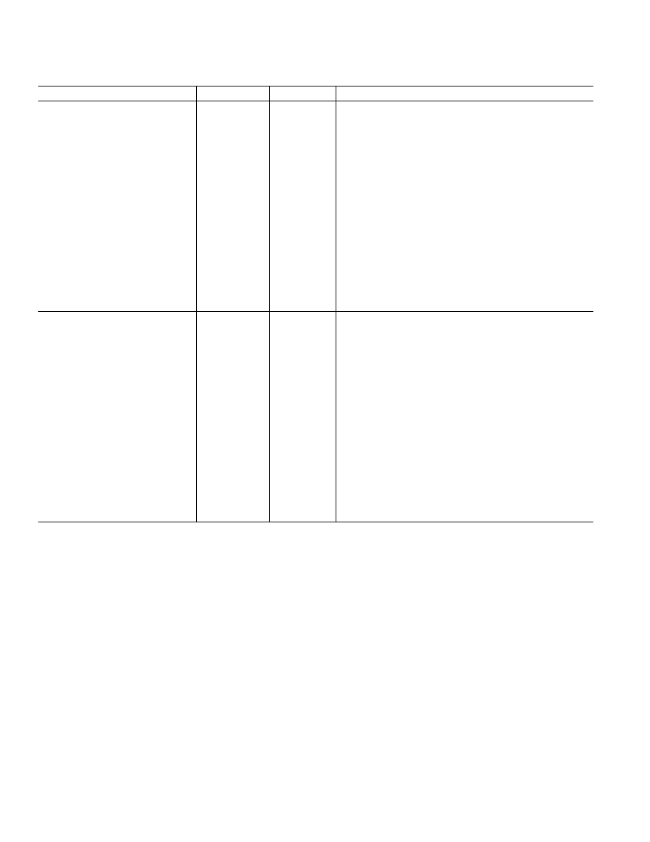
Parameter
A, S Versions
1
Units
Conditions/Comments
STATIC PERFORMANCE
No Missing Codes
24
Bits min
Guaranteed by Design. For Filter Notches
12 Hz
22
Bits min
For Filter Notch = 20 Hz
18
Bits min
For Filter Notch = 50 Hz
15
Bits min
For Filter Notch = 100 Hz
12
Bits min
For Filter Notch = 200 Hz
Output Noise
See Tables I & II
Depends on Filter Cutoffs and Selected Gain
Integral Nonlinearity
±
0.0015
% of FSR max
Filter Notches
12 Hz; Typically
±
0.0003%
Positive Full-Scale Error
2, 3
See Note 4
Full-Scale Drift
5
1
µ
V/
°
C typ
For Gains of 1, 2
0.3
µ
V/
°
C typ
For Gains of 4, 8, 16, 32, 64, 128
Unipolar Offset Error
2
See Note 4
Unipolar Offset Drift
5
0.5
µ
V/
°
C typ
For Gains of 1, 2
0.25
µ
V/
°
C typ
For Gains of 4, 8, 16, 32, 64, 128
Bipolar Zero Error
2
See Note 4
Bipolar Zero Drift
5
0.5
µ
V/
°
C typ
For Gains of 1, 2
0.25
µ
V/
°
C typ
For Gains of 4, 8, 16, 32, 64, 128
Gain Drift
2
ppm/
°
C typ
Bipolar Negative Full-Scale Error
2
±
0.004
% of FSR max
Typically
±
0.0006%
Bipolar Negative Full-Scale Drift
5
1
µ
V/
°
C typ
For Gains of 1, 2
0.3
µ
V/
°
C typ
For Gains of 4, 8, 16, 32, 64, 128
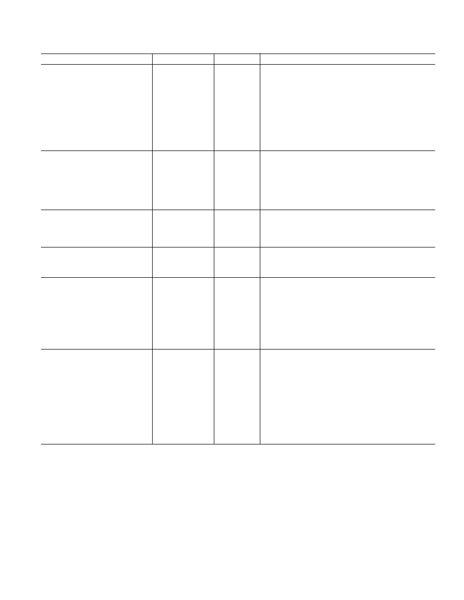
ANALOG INPUTS
Input Sampling Rate, f
S
See Table III
Normal-Mode 50 Hz Rejection
6
100
dB min
For Filter Notches of 2 Hz, 5 Hz, 10 Hz, 25 Hz, 50 Hz,
±
0.02
×
f
NOTCH
Normal-Mode 60 Hz Rejection
6
100
dB min
For Filter Notches of 2 Hz, 6 Hz, 10 Hz, 30 Hz, 60 Hz,
±
0.02
×
f
NOTCH
AIN1, AIN2
7
Input Voltage Range
8
For Normal Operation. Depends on Gain Selected.
0 to +V
REF
9
V max
Unipolar Input Range (B/U Bit of Control Register = 1)
±
V
REF
V max
Bipolar Input Range (B/U Bit of Control Register = 0)
Common-Mode Rejection (CMR)
100
dB min
At DC
Common-Mode 50 Hz Rejection
6
150
dB min
For Filter Notches of 2 Hz, 5 Hz, 10 Hz, 25 Hz, 50 Hz,
±
0.02
×
f
NOTCH
Common-Mode 60 Hz Rejection
6
150
dB min
For Filter Notches of 2 Hz, 6 Hz, 10 Hz, 30 Hz, 60 Hz,
±
0.02
×
f
NOTCH
Common-Mode Voltage Range
10
AGND to AV
DD
V min to V max
DC Input Leakage Current @ +25
°
C
10
pA max
T
MIN
to T
MAX
1
nA max
Sampling Capacitance
6
20
pF max
AIN3
Input Voltage Range
0 to + 4
×
V
REF
V max
For Normal Operation. Depends on Gain Selected
Gain Error
11
±
0.05
% typ
Additional Error Contributed by Resistor Attenuator
Gain Drift
1
ppm/
°
C typ
Additional Drift Contributed by Resistor Attenuator
Offset Error
11
4
mV max
Additional Error Contributed by Resistor Attenuator
Input Impedance
30
k
min
NOTES
1
Temperature range is as follows: A Version, 40
°
C to +85
°
C; S Version, 55
°
C to +125
°
C.
2
Applies after calibration at the temperature of interest.
3
Positive full-scale error applies to both unipolar and bipolar input ranges.
4
These errors will be of the order of the output noise of the part as shown in Table I after system calibration. These errors will be 20
µ
V typical after self-calibration
or background calibration.
5
Recalibration at any temperature or use of the background calibration mode will remove these drift errors.
6
These numbers are guaranteed by design and/or characterization.
7
The AIN1 and AIN2 analog inputs presents a very high impedance dynamic load which varies with clock frequency and input sample rate. The maximum
recommended source resistance depends on the selected gain.
8
The analog input voltage range on the AIN1(+) and AIN2(+) inputs is given here with respect to the voltage on the AIN1() and AIN2 () inputs. The input
voltage range on the AIN3 input is with respect to AGND. The absolute voltage on the AIN1 and AIN2 inputs should not go more positive than A V
DD
+ 30 mV or
more negative than AGND 30 mV.
9
V
REF
= REF IN(+) REF IN().
10
This common-mode voltage range is allowed provided that the input voltage on AIN(+) and AIN() does not exceed A V
DD
+ 30 mV and AGND 30 mV.
11
This error can be removed using the system calibration capabilities of the AD7713. This error is not removed by the AD7713's self-calibration feature. The offset
drift on the AIN3 input is four times the value given in the Static Performance section.
2
REV. C
(AV
DD
= +5 V
5%; DV
DD
= +5 V 5%; REF IN(+) = +2.5 V; REF IN() = AGND;
MCLK IN = 2 MHz unless otherwise noted. All specifications T
MIN
to T
MAX
unless otherwise noted.)
AD7713SPECIFICATIONS
Parameter
A, S Versions
1
Units
Conditions/Comments
REFERENCE INPUT
REF IN(+) REF IN() Voltage
+2.5 to AV
DD
/1.8
V min to V max
For Specified Performance. Part Is Functional with Lower
V
REF
Voltages
Input Sampling Rate, f
S
f
CLK IN
/512
Normal-Mode 50 Hz Rejection
6
100
dB min
For Filter Notches of 2 Hz, 5 Hz, 10 Hz, 25 Hz, 50 Hz,
±
0.02
×
f
NOTCH
Normal-Mode 60 Hz Rejection
6
100
dB min
For Filter Notches of 2 Hz, 6 Hz, 10 Hz, 30 Hz, 60 Hz,
±
0.02
×
f
NOTCH
Common-Mode Rejection (CMR)
100
dB min
At DC
Common-Mode 50 Hz Rejection
6
150
dB min
For Filter Notches of 2 Hz, 5 Hz, 10 Hz, 25 Hz, 50 Hz,
±
0.02
×
f
NOTCH
Common-Mode 60 Hz Rejection
6
150
dB min
For Filter Notches of 2 Hz, 6 Hz, 10 Hz, 30 Hz, 60 Hz,
±
0.02
×
f
NOTCH
Common-Mode Voltage Range
10
AGND to AV
DD
V min to V max
DC Input Leakage Current @ +25
°
C
10
pA max
T
MIN
to T
MAX
1
nA max
LOGIC INPUTS
Input Current
±
10
µ
A max
All Inputs Except MCLK IN
V
INL
, Input Low Voltage
0.8
V max
V
INH
, Input High Voltage
2.0
V min
MCLK IN Only
V
INL
, Input Low Voltage
0.8
V max
V
INH
, Input High Voltage
3.5
V min
LOGIC OUTPUTS
V
OL
, Output Low Voltage
0.4
V max
I
SINK
= 1.6 mA
V
OH
, Output High Voltage
4.0
V min
I
SOURCE
= 100
µ
A
Floating State Leakage Current
±
10
µ
A max
Floating State Output Capacitance
12
9
pF typ
TRANSDUCER BURN-OUT
Current
1
µ
A nom
Initial Tolerance @ +25
°
C
±
10
% typ
Drift
0.1
%/
°
C typ
RTD EXCITATION CURRENTS
(RTD1, RTD2)
Output Current
200
µ
A nom
Initial Tolerance @ +25
°
C
±
20
% max
Drift
20
ppm/
°
C typ
Initial Matching @ +25
°
C
±
1
% max
Matching Between RTD1 and RTD2 Currents
Drift Matching
3
ppm/
°
C typ
Matching Between RTD1 and RTD2 Current Drift
Line Regulation (AV
DD
)
200
nA/V max
AV
DD
= +5 V
Load Regulation
200
nA/V max
SYSTEM CALIBRATION
AIN1, AIN2
Positive Full-Scale Calibration Limit
13
+(1.05
×
V
REF
)/GAIN
V max
GAIN Is the Selected PGA Gain (Between 1 and 128)
Negative Full-Scale Calibration Limit
13
(1.05
×
V
REF
)/GAIN
V max
GAIN Is the Selected PGA Gain (Between 1 and 128)
Offset Calibration Limit
14, 15
(1.05
×
V
REF
)/GAIN
V max
GAIN Is the Selected PGA Gain (Between 1 and 128)
Input Span
14
+0.8
×
V
REF
/GAIN
V min
GAIN Is the Selected PGA Gain (Between 1 and 128)
+(2.1
×
V
REF
)/GAIN
V max
GAIN Is the Selected PGA Gain (Between 1 and 128)
AIN3
Positive Full-Scale Calibration Limit
13
+(4.2
×
V
REF
)/GAIN
V max
GAIN Is the Selected PGA Gain (Between 1 and 128)
Offset Calibration Limit
15
0 to V
REF
/GAIN
V max
GAIN Is the Selected PGA Gain (Between 1 and 128)
Input Span
+3.2
×
V
REF
/GAIN
V min
GAIN Is the Selected PGA Gain (Between 1 and 128)
+(4.2
×
V
REF
)/GAIN
V max
GAIN Is the Selected PGA Gain (Between 1 and 128)
NOTES
12
Guaranteed by design, not production tested.
13
After calibration, if the analog input exceeds positive full scale, the converter will output all 1s. If the analog input is less than negative full scale, then the device will
output all 0s.
14
These calibration and span limits apply provided the absolute voltage on the AIN1 and AIN2 analog inputs does not exceed AV
DD
+ 30 mV or go more negative
than AGND 30 mV.
15
The offset calibration limit applies to both the unipolar zero point and the bipolar zero point.
AD7713
3
REV. C
Parameter
A, S Versions
1
Units
Conditions/Comments
POWER REQUIREMENTS
Power Supply Voltages
AV
DD
Voltage
+5 to +10
V nom
±
5% for Specified Performance
DV
DD
Voltage
16
+5
V nom
±
5% for Specified Performance
Power Supply Currents
AV
DD
Current
0.6
mA max
AV
DD
= +5 V
0.7
mA max
AV
DD
= +10 V
DV
DD
Current
0.5
mA max
f
CLK IN
= 1 MHz. Digital Inputs 0 V to DV
DD
1
mA max
f
CLK IN
= 2 MHz. Digital Inputs 0 V to DV
DD
Power Supply Rejection
17
Rejection w.r.t. AGND
(AV
DD
and DV
DD
)
See Note 18
dB typ
Power Dissipation
Normal Mode
5.5
mW max
AV
DD
= DV
DD
= +5 V, f
CLK IN
= 1 MHz; Typically 3.5 mW
Standby (Power-Down) Mode
300
µ
W max
AV
DD
= DV
DD
= +5 V, Typically 150
µ
W
NOTES
16
The
±
5% tolerance on the DV
DD
input is allowed provided that DV
DD
does not exceed AV
DD
by more than 0.3 V.
17
Measured at dc and applies in the selected passband. PSRR at 50 Hz will exceed 120 dB with filter notches of 2 Hz, 5 Hz, 10 Hz, 25 Hz or 50 Hz. PSRR at 60 Hz
will exceed 120 dB with filter notches of 2 Hz, 6 Hz, 10 Hz, 30 Hz or 60 Hz.
18
PSRR depends on gain: gain of 1 = 70 dB typ; gain of 2 = 75 dB typ; gain of 4 = 80 dB typ; gains of 8 to 128 = 85 dB typ.
Specifications subject to change without notice.
AD7713SPECIFICATIONS
REV. C
4
TIMING CHARACTERISTICS
1, 2
Limit at T
MIN
, T
MAX
Parameter
(A, S Versions)
Units
Conditions/Comments
f
CLK IN
3, 4
400
kHz min
Master Clock Frequency: Crystal Oscillator or
2
MHz max
Externally Supplied for Specified Performance
t
CLK IN LO
0.4
×
t
CLK IN
ns min
Master Clock Input Low Time; t
CLK IN
= 1/f
CLK IN
t
CLK IN HI
0.4
×
t
CLK IN
ns min
Master Clock Input High Time
t
r
5
50
ns max
Digital Output Rise Time; Typically 20 ns
t
f
5
50
ns max
Digital Output Fall Time; Typically 20 ns
t
1
1000
ns min
SYNC
Pulse Width
Self-Clocking Mode
t
2
0
ns min
DRDY
to RFS Setup Time
t
3
0
ns min
DRDY
to RFS Hold Time
t
4
2
×
t
CLK IN
ns min
A0 to RFS Setup Time
t
5
0
ns min
A0 to RFS Hold Time
t
6
4
×
t
CLK IN
+ 20
ns max
RFS
Low to SCLK Falling Edge
t
7
6
4
×
t
CLK IN
+20
ns max
Data Access Time (RFS Low to Data Valid)
t
8
6
t
CLK IN
/2
ns min
SCLK Falling Edge to Data Valid Delay
t
CLK IN
/2
+ 30
ns max
t
9
t
CLK IN
/2
ns nom
SCLK High Pulse Width
t
10
3
×
t
CLK IN
/2
ns nom
SCLK Low Pulse Width
t
14
50
ns min
A0 to TFS Setup Time
t
15
0
ns min
A0 to TFS Hold Time
t
16
4
×
t
CLK IN
+ 20
ns max
TFS
to SCLK Falling Edge Delay Time
t
17
4
×
t
CLK IN
ns min
TFS
to SCLK Falling Edge Hold Time
t
18
0
ns min
Data Valid to SCLK Setup Time
t
19
10
ns min
Data Valid to SCLK Hold Time
(DV
DD
= +5 V
±
5%; AV
DD
= +5 V or +10 V
±
5%; AGND = DGND = 0 V; f
CLKIN
=2 MHz;
Input Logic 0 = 0 V, Logic 1 = DV
DD
unless otherwise noted.)
2
5
REV. C
AD7713
Limit at T
MIN
, T
MAX
Parameter
(A, S Versions)
Units
Conditions/Comments
External-Clocking Mode
f
SCLK
f
CLK IN
/5
MHz max
Serial Clock Input Frequency
t
20
0
ns min
DRDY
to RFS Setup Time
t
21
0
ns min
DRDY
to RFS Hold Time
t
22
2
×
t
CLK IN
ns min
A0 to RFS Setup Time
t
23
0
ns min
A0 to RFS Hold Time
t
24
6
4
×
t
CLK IN
ns max
Data Access Time (RFS Low to Data Valid)
t
25
6
10
ns min
SCLK Falling Edge to Data Valid Delay
2
×
t
CLK IN
+ 20
ns max
t
26
2
×
t
CLK IN
ns min
SCLK High Pulse Width
t
27
2
×
t
CLK IN
ns min
SCLK Low Pulse Width
t
28
t
CLK IN
+ 10
ns max
SCLK Falling Edge to DRDY High
t
29
7
10
ns min
SCLK to Data Valid Hold Time
t
CLK IN
+ 10
ns max
t
30
10
ns min
RFS
/TFS to SCLK Falling Edge Hold Time
t
31
7
5
×
t
CLK IN
/2 + 50
ns max
RFS
to Data Valid Hold Time
t
32
0
ns min
A0 to TFS Setup Time
t
33
0
ns min
A0 to TFS Hold Time
t
34
4
×
t
CLK IN
ns min
SCLK Falling Edge to TFS Hold Time
t
35
2
×
t
CLK IN
SCLK High
ns min
Data Valid to SCLK Setup Time
t
36
30
ns min
Data Valid to SCLK Hold Time
NOTES
1
Guaranteed by design, not production tested. All input signals are specified with tr = tf = 5 ns (10% to 90% of 5 V) and timed from a voltage level of 1.6 V.
2
See Figures 10 to 13.
3
CLK IN duty cycle range is 45% to 55%. CLK IN must be supplied whenever the AD7713 is not in STANDBY mode. If no clock is present in this case, the
device can draw higher current than specified and possibly become uncalibrated.
4
The AD7713 is production tested with f
CLK IN
at 2 MHz. It is guaranteed by characterization to operate at 400 kHz.
5
Specified using 10% and 90% points on waveform of interest.
6
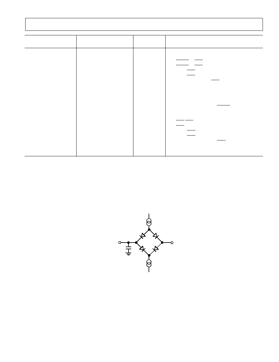
These numbers are measured with the load circuit of Figure 1 and defined as the time required for the output to cross 0.8 V or 2.4 V.
7
These numbers are derived from the measured time taken by the data output to change 0.5 V when loaded with the circuit of Figure 1. The measured number
is then extrapolated back to remove effects of charging or discharging the 100 pF capacitor. This means that the times quoted in the timing characteristics are
the true bus relinquish times of the part and, as such, are independent of external bus loading capacitances.
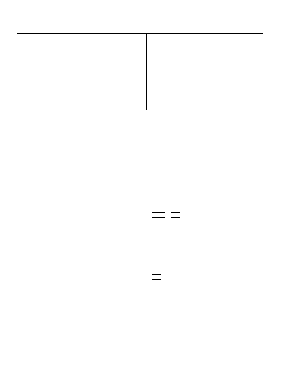
TO OUTPUT
PIN
+2.1V
1.6mA
200µA
100pF
Figure 1. Load Circuit for Access Time and Bus Relinquish Time