Äîêóìåíòàöèÿ è îïèñàíèÿ www.docs.chipfind.ru
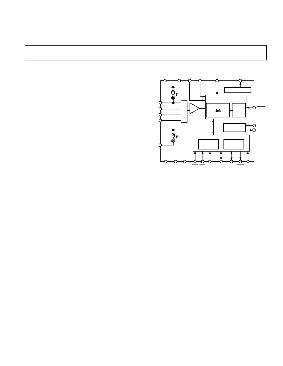
FUNCTIONAL BLOCK DIAGRAM
REV. F
Information furnished by Analog Devices is believed to be accurate and
reliable. However, no responsibility is assumed by Analog Devices for its
use, nor for any infringements of patents or other rights of third parties
which may result from its use. No license is granted by implication or
otherwise under any patent or patent rights of Analog Devices.
a
Signal Conditioning ADC
AD7710*
FEATURES
Charge Balancing ADC
24 Bits No Missing Codes
0.0015% Nonlinearity
Two-Channel Programmable Gain Front End
Gains from 1 to 128
Differential Inputs
Low-Pass Filter with Programmable Filter Cutoffs
Ability to Read/Write Calibration Coefficients
Bidirectional Microcontroller Serial Interface
Internal/External Reference Option
Single or Dual Supply Operation
Low Power (25 mW typ) with Power-Down Mode
(7 mW typ)
APPLICATIONS
Weigh Scales
Thermocouples
Process Control
Smart Transmitters
Chromatography
GENERAL DESCRIPTION
The AD7710 is a complete analog front end for low frequency
measurement applications. The device accepts low level signals
directly from a strain gage or transducer and outputs a serial
digital word. It employs a sigma-delta conversion technique to
realize up to 24 bits of no missing codes performance. The input
signal is applied to a proprietary programmable gain front end
based around an analog modulator. The modulator output is
processed by an on-chip digital filter. The first notch of this
digital filter can be programmed via the on-chip control register
allowing adjustment of the filter cutoff and settling time.
The part features two differential analog inputs and a differen-
tial reference input. Normally, one of the channels will be used
as the main channel with the second channel used as an auxil-
iary input to periodically measure a second voltage. It can be
operated from a single supply (by tying the V
SS
pin to AGND)
provided that the input signals on the analog inputs are more
positive than 30 mV. By taking the V
SS
pin negative, the part
can convert signals down to V
REF
on its inputs. The AD7710
thus performs all signal conditioning and conversion for a single
or dual channel system.
The AD7710 is ideal for use in smart, microcontroller based
systems. Input channel selection, gain settings and signal polar-
ity can be configured in software using the bidirectional serial
port. The AD7710 contains self-calibration, system calibration
and background calibration options and also allows the user to
read and write the on-chip calibration registers.
*Protected by U.S. Patent No. 5,134,401.
CMOS construction ensures low power dissipation and a soft-
ware programmable power down mode reduces the standby
power consumption to only 7 mW typical. The part is available
in a 24-lead, 0.3 inch-wide, plastic and hermetic dual-in-line
package (DIP) as well as a 24-lead small outline (SOIC)
package.
PRODUCT HIGHLIGHTS
1. The programmable gain front end allows the AD7710 to
accept input signals directly from a strain gage or transducer,
removing a considerable amount of signal conditioning.
2. The AD7710 is ideal for microcontroller or DSP processor
applications with an on-chip control register which allows
control over filter cutoff, input gain, channel selection, signal
polarity and calibration modes.
3. The AD7710 allows the user to read and write the on-chip
calibration registers. This means that the microcontroller has
much greater control over the calibration procedure.
4. No missing codes ensures true, usable, 23-bit dynamic range
coupled with excellent
±
0.0015% accuracy. The effects of
temperature drift are eliminated by on-chip self-calibration,
which removes zero-scale and full-scale errors.
One Technology Way, P.O. Box 9106, Norwood, MA 02062-9106, U.S.A.
Tel: 781/329-4700
World Wide Web Site: http://www.analog.com
Fax: 781/326-8703
© Analog Devices, Inc., 1999
CLOCK
GENERATION
SERIAL INTERFACE
CONTROL
REGISTER
OUTPUT
REGISTER
CHARGE-BALANCING A/D
CONVERTER
AUTO-ZEROED
MODULATOR
DIGITAL
FILTER
AD7710
M
U
X
PGA
AGND DGND
MODE SDATA SCLK
A0
MCLK
OUT
MCLK
IN
AIN1(+)
AIN1()
REF
IN ()
REF
IN (+)
SYNC
4.5 A
A = 1 128
DRDY
TFS
RFS
REF OUT
2.5V REFERENCE
AV
DD
AV
DD
20 A
AIN2(+)
AIN2()
I
OUT
V
SS
V
BIAS
AV
DD
DV
DD

REV. F
2
Parameter
A, S Versions
1
Units
Conditions/Comments
STATIC PERFORMANCE
No Missing Codes
24
Bits min
Guaranteed by Design. For Filter Notches
60 Hz
22
Bits min
For Filter Notch = 100 Hz
18
Bits min
For Filter Notch = 250 Hz
15
Bits min
For Filter Notch = 500 Hz
12
Bits min
For Filter Notch = 1 kHz
Output Noise
Tables I and II
Depends on Filter Cutoffs and Selected Gain
Integral Nonlinearity @ +25
°
C
±
0.0015
% of FSR max
Filter Notches
60 Hz
T
MIN
to T
MAX
±
0.003
% of FSR max
Typically
±
0.0003%
Positive Full-Scale Error
2,
3
See Note 4
Excluding Reference
Full-Scale Drift
5
1
µ
V/
°
C typ
Excluding Reference. For Gains of 1, 2
0.3
µ
V/
°
C typ
Excluding Reference. For Gains of 4, 8, 16, 32, 64, 128
Unipolar Offset Error
2
See Note 4
Unipolar Offset Drift
5
0.5
µ
V/
°
C typ
For Gains of 1, 2
0.25
µ
V/
°
C typ
For Gains of 4, 8, 16, 32, 64, 128
Bipolar Zero Error
2
See Note 4
Bipolar Zero Drift
5
0.5
µ
V/
°
C typ
For Gains of 1, 2
0.25
µ
V/
°
C typ
For Gains of 4, 8, 16, 32, 64, 128
Gain Drift
2
ppm/
°
C typ
Bipolar Negative Full-Scale Error
2
@ +25
°
C
±
0.003
% of FSR max
Excluding Reference
T
MIN
to T
MAX
±
0.006
% of FSR max
Typically
±
0.0006%
Bipolar Negative Full-Scale Drift
5
1
µ
V/
°
C typ
Excluding Reference. For Gains of 1, 2
0.3
µ
V/
°
C typ
Excluding Reference. For Gains of 4, 8, 16, 32, 64, 128
ANALOG INPUTS/REFERENCE INPUTS
Input Common-Mode Rejection (CMR)
100
dB min
At DC and AV
DD
= 5 V
90
dB min
At DC and AV
DD
= 10 V
Common-Mode Voltage Range
6
V
SS
to AV
DD
V min to V max
Normal-Mode 50 Hz Rejection
7
100
dB min
For Filter Notches of 10, 25, 50 Hz,
±
0.02
×
f
NOTCH
Normal-Mode 60 Hz Rejection
7
100
dB min
For Filter Notches of 10, 30, 60 Hz,
±
0.02
×
f
NOTCH
Common-Mode 50 Hz Rejection
7
150
dB min
For Filter Notches of 10, 25, 50 Hz,
±
0.02
×
f
NOTCH
Common-Mode 60 Hz Rejection
7
150
dB min
For Filter Notches of 10, 30, 60 Hz,
±
0.02
×
f
NOTCH
DC Input Leakage Current
7
@ +25
°
C
10
pA max
T
MIN
to T
MAX
1
nA max
Sampling Capacitance
7
20
pF max
Analog Inputs
8
Input Voltage Range
9
For Normal Operation. Depends on Gain Selected
0 to +V
REF
10
nom
Unipolar Input Range (B/U Bit of Control Register = 1)
±
V
REF
nom
Bipolar Input Range (B/U Bit of Control Register = 0)
Input Sampling Rate, f
S
See Table III
Reference Inputs
REF IN(+) REF IN() Voltage
11
+2.5 to +5
V min to V max For Specified Performance. Part Is Functional with
Lower V
REF
Voltages
Input Sampling Rate, f
S
f
CLK IN
/256
NOTES
1
Temperature ranges are as follows: A Version, 40
°
C to +85
°
C; S Version, 55
°
C to +125
°
C. See also Note 16.
2
Applies after calibration at the temperature of interest.
3
Positive full-scale error applies to both unipolar and bipolar input ranges.
4
These errors will be of the order of the output noise of the part as shown in Table I after system calibration. These errors will be 20
µ
V typical after self-calibration
or background calibration.
5
Recalibration at any temperature or use of the background calibration mode will remove these drift errors.
6
This common-mode voltage range is allowed provided that the input voltage on AIN(+) and AIN() does not exceed AV
DD
+ 30 mV and V
SS
30 mV.
7
These numbers are guaranteed by design and/or characterization.
8
The analog inputs present a very high impedance dynamic load which varies with clock frequency and input sample rate. The maximum recommended source
resistance depends on the selected gain (see Tables IV and V).
9
The analog input voltage range on the AIN1(+) and AIN2(+) inputs is given here with respect to the voltage on the AIN1() and AIN2() inputs. The absolute
voltage on the analog inputs should not go more positive than AV
DD
+ 30 mV or go more negative than V
SS
30 mV.
10
V
REF
= REF IN(+) REF IN().
11
The reference input voltage range may be restricted by the input voltage range requirement on the V
BIAS
input.
AD7710SPECIFICATIONS
(AV
DD
= +5 V 5%; DV
DD
= +5 V 5%; V
SS
= 0 V or 5 V 5%; REF IN(+) = +2.5 V;
REF IN() = AGND; MCLK IN = 10 MHz unless otherwise noted. All specifications T
MIN
to T
MAX
unless otherwise noted.)

Parameter
A, S Versions
1
Units
Conditions/Comments
REFERENCE OUTPUT
Output Voltage
2.5
V nom
Initial Tolerance @ +25
°
C
±
1
% max
Drift
20
ppm/
°
C typ
Output Noise
30
µ
V typ
pk-pk Noise 0.1 Hz to 10 Hz Bandwidth
Line Regulation (AV
DD
)
1
mV/V max
Load Regulation
1.5
mV/mA max Maximum Load Current 1 mA
External Current
1
mA max
V
BIAS
INPUT
12
Input Voltage Range
AV
DD
0.85
×
V
REF
See V
BIAS
Input Section
or AV
DD
3.5
V max
Whichever Is Smaller: +5 V/5 V or +10 V/0 V
Nominal AV
DD
/V
SS
or AV
DD
2.1
V max
Whichever Is Smaller; +5 V/0 V Nominal AV
DD
/V
SS
V
SS
+ 0.85
×
V
REF
See V
BIAS
Input Section
or V
SS
+ 3
V min
Whichever Is Greater; +5 V/5 V or +10 V/0 V
Nominal AV
DD
/V
SS
or V
SS
+ 2.1
V min
Whichever Is Greater; +5 V/0 V Nominal AV
DD
/V
SS
V
BIAS
Rejection
65 to 85
dB typ
Increasing with Gain
LOGIC INPUTS
Input Current
±
10
µ
max
All Inputs Except MCLK IN
V
INL
, Input Low Voltage
0.8
V max
V
INH
, Input High Voltage
2.0
V min
MCLK IN Only
V
INL
, Input Low Voltage
0.8
V max
V
INH
, Input High Voltage
3.5
V min
LOGIC OUTPUTS
V
OL
, Output Low Voltage
0.4
V max
I
SINK
= 1.6 mA
V
OH
, Output High Voltage
DV
DD
1
V min
I
SOURCE
= 100
µ
A
Floating State Leakage Current
±
10
µ
A max
Floating State Output Capacitance
13
9
pF typ
TRANSDUCER BURNOUT
Current
4.5
µ
A nom
Initial Tolerance @ +25
°
C
±
10
% typ
Drift
0.1
%/
°
C typ
COMPENSATION CURRENT
Output Current
20
µ
A nom
Initial Tolerance @ +25
°
C
±
4
µ
A max
Drift
35
ppm/
°
C typ
Line Regulation (AV
DD
)
20
nA/V max
AV
DD
= +5 V
Load Regulation
20
nA/V max
Output Compliance
AV
DD
2
V max
SYSTEM CALIBRATION
Positive Full-Scale Calibration Limit
l4
(1.05
×
V
REF
)/GAIN
V max
GAIN Is the Selected PGA Gain (Between 1 and 128)
Negative Full-Scale Calibration Limit
l4
(1.05
×
V
REF
)/GAIN
V max
GAIN Is the Selected PGA Gain (Between 1 and 128)
Offset Calibration Limits
15
(1.05
×
V
REF
)/GAIN
V max
GAIN Is the Selected PGA Gain (Between 1 and 128)
Input Span
15
0.8
×
V
REF
/GAIN
V min
GAIN Is the Selected PGA Gain (Between 1 and 128)
(2.1
×
V
REF
)/GAIN
V max
GAIN Is the Selected PGA Gain (Between 1 and 128)
NOTES
12
The AD7710 is tested with the following V
BIAS
voltages. With AV
DD
= +5 V and V
SS
= 0 V, V
BIAS
= +2.5 V; with AV
DD
= +10 V and V
SS
= 0 V, V
BIAS
= +5 V and
with AV
DD
= +5 V and V
SS
= 5 V, V
BIAS
= 0 V.
13
Guaranteed by design, not production tested.
14
After calibration, if the analog input exceeds positive full scale, the converter will output all 1s. If the analog input is less than negative full scale then the device will
output all 0s.
15
These calibration and span limits apply provided the absolute voltage on the analog inputs does not exceed AV
DD
+ 30 mV or go more negative than V
SS
30 mV.
The offset calibration limit applies to both the unipolar zero point and the bipolar zero point.
REV. F
3
AD7710
ORDERING GUIDE
Temperature
Package
Model
1
Range
Options
2
AD7710AN
40
°
C to +85
°
C
N-24
AD7710AR
40
°
C to +85
°
C
R-24
AD7710AQ
40
°
C to +85
°
C
Q-24
AD7710SQ
55
°
C to +125
°
C
Q-24
EVAL-AD7710EB
Evaluation Board
NOTES
1
To order MIL-STD-883B, Class B processed parts, add /883B to par number.
Contact our local sales office for military data sheet and availability.
2
N = Plastic DIP; Q = Cerdip; R = SOIC.
Parameter
A, S Versions
l
Units
Conditions/Comments
POWER REQUIREMENTS
Power Supply Voltages
AV
DD
Voltage
16
+5 to +10
V nom
±
5% for Specified Performance
DV
DD
Voltage
17
+5
V nom
±
5% for Specified Performance
AV
DD
-V
SS
Voltage
+10.5
V max
For Specified Performance
Power Supply Currents
AV
DD
Current
4
mA max
DV
DD
Current
4.5
mA max
V
SS
Current
1.5
mA max
V
SS
= 5 V
Power Supply Rejection
18
Rejection w.r.t. AGND; Assumes V
BIAS
Is Fixed
Positive Supply (AV
DD
& DV
DD
)
See Note 19
dB typ
Negative Supply (V
SS
)
90
dB typ
Power Dissipation
Normal Mode
45
mW max
AV
DD
= DV
DD
= +5 V, V
SS
= 0 V; Typically 25 mW
52.5
mW max
AV
DD
= DV
DD
= +5 V, V
SS
= 5 V; Typically 30 mW
Standby (Power-Down) Mode
15
mW max
AV
DD
= DV
DD
= +5 V, V
SS
= 0 V or 5 V; Typically 7 mW
NOTES
16
The AD7710 is specified with a 10 MHz clock for AV
DD
voltages of +5 V
±
5%. It is specified with an 8 MHz clock for AV
DD
voltages greater than 5.25 V and less
than 10.5 V.
17
The
±
5% tolerance on the DV
DD
input is allowed provided that DV
DD
does not exceed AV
DD
by more than 0.3 V.
18
Measured at dc and applies in the selected passband. PSRR at 50 Hz will exceed 120 dB with filter notches of 10 Hz, 25 Hz or 50 Hz. PSRR at 60 Hz will exceed
120 dB with filter notches of 10 Hz, 30 Hz or 60 Hz.
19
PSRR depends on gain: Gain of 1: 70 dB typ; Gain of 2: 75 dB typ; Gain of 4: 80 dB typ; Gains of 8 to 128: 85 dB typ. These numbers can be improved ( to 95 dB
typ) by deriving the V
BIAS
voltage (via Zener diode or reference) from the AV
DD
supply.
Specifications subject to change without notice.
Digital Input Voltage to DGND . . . . . 0.3 V to AV
DD
+ 0.3 V
Digital Output Voltage to DGND . . . . 0.3 V to DV
DD
+ 0.3 V
Operating Temperature Range
Commercial (A Version) . . . . . . . . . . . . . . . 40
°
C to +85
°
C
Extended (S Version) . . . . . . . . . . . . . . . . . 55
°
C to +125
°
C
Storage Temperature Range . . . . . . . . . . . . . 65
°
C to +150
°
C
Lead Temperature (Soldering, 10 secs) . . . . . . . . . . . . +300
°
C
Power Dissipation (Any Package) to +75
°
C . . . . . . . . 450 mW
Derates Above +75
°
C . . . . . . . . . . . . . . . . . . . . . . . . 6 mW/
°
C
*Stresses above those listed under Absolute Maximum Ratings may cause
permanent damage to the device. This is a stress rating only; functional operation
of the device at these or any other conditions above those listed in the operational
sections of the specification is not implied. Exposure to absolute maximum rating
conditions for extended periods may affect device reliability.
ABSOLUTE MAXIMUM RATINGS*
(T
A
= +25
°
C, unless otherwise noted)
AV
DD
to DV
DD
. . . . . . . . . . . . . . . . . . . . . . . . . . 0.3 V to +12 V
AV
DD
to V
SS
. . . . . . . . . . . . . . . . . . . . . . . . . . . . .0.3 V to +12 V
AV
DD
to AGND . . . . . . . . . . . . . . . . . . . . . . . . . 0.3 V to +12 V
AV
DD
to DGND . . . . . . . . . . . . . . . . . . . . . . . . . 0.3 V to +12 V
DV
DD
to AGND . . . . . . . . . . . . . . . . . . . . . . . . . . 0.3 V to +6 V
DV
DD
to DGND . . . . . . . . . . . . . . . . . . . . . . . . . . 0.3 V to +6 V
V
SS
to AGND . . . . . . . . . . . . . . . . . . . . . . . . . . . .+0.3 V to 6 V
V
SS
to DGND . . . . . . . . . . . . . . . . . . . . . . . . . . . .+0.3 V to 6 V
Analog Input Voltage to AGND
. . . . . . . . . . . . . . . . . . . . . . . . . . . V
SS
0.3 V to AV
DD
+ 0.3 V
Reference Input Voltage to AGND
. . . . . . . . . . . . . . . . . . . . . . . . . . . V
SS
0.3 V to AV
DD
+ 0.3 V
REF OUT to AGND . . . . . . . . . . . . . . . . . . . . . . 0.3 V to AV
DD
AD7710SPECIFICATIONS
REV. F
4
CAUTION
ESD (electrostatic discharge) sensitive device. Electrostatic charges as high as 4000 V readily
accumulate on the human body and test equipment and can discharge without detection.
Although the AD7710 features proprietary ESD protection circuitry, permanent damage may
occur on devices subjected to high energy electrostatic discharges. Therefore, proper ESD
precautions are recommended to avoid performance degradation or loss of functionality.
WARNING!
ESD SENSITIVE DEVICE
AD7710
REV. F
5
(DV
DD
= +5 V 5%; AV
DD
= +5 V or +10 V
3
5%; V
SS
= 0 V or 5 V 10%; AGND = DGND =
0 V; f
CLK IN
=10 MHz; Input Logic 0 = 0 V, Logic 1 = DV
DD
, unless otherwise noted)
TIMING CHARACTERISTICS
1,
2
Limit at T
MIN
, T
MAX
Parameter
(A, S Versions)
Units
Conditions/Comments
f
CLK IN
4,
5
Master Clock Frequency: Crystal Oscillator or Externally
400
kHz min
Supplied for Specified Performance
10
MHz max
AV
DD
= +5 V
±
5%
8
MHz max
AV
DD
= +5.25 V to +10.5 V
t
CLK IN LO
0.4
×
t
CLK IN
ns min
Master Clock Input Low Time. t
CLK IN
= 1/f
CLK IN
t
CLK IN HI
0.4
×
t
CLK IN
ns min
Master Clock Input High Time
t
r
6
50
ns max
Digital Output Rise Time. Typically 20 ns
t
f
6
50
ns max
Digital Output Fall Time. Typically 20 ns
t
1
1000
ns min
SYNC Pulsewidth
Self-Clocking Mode
t
2
0
ns min
DRDY to RFS Setup Time
t
3
0
ns min
DRDY to RFS Hold Time
t
4
2
×
t
CLK IN
ns min
A0 to
RFS Setup Time
t
5
0
ns min
A0 to
RFS Hold Time
t
6
4
×
t
CLK IN
+ 20
ns max
RFS Low to SCLK Falling Edge
t
7
7
4
×
t
CLK IN
+ 20
ns max
Data Access Time (
RFS Low to Data Valid)
t
8
7
t
CLK IN
/2
ns min
SCLK Falling Edge to Data Valid Delay
t
CLK IN
/2 + 30
ns max
t
9
t
CLK IN
/2
ns nom
SCLK High Pulsewidth
t
10
3
×
t
CLK IN
/2
ns nom
SCLK Low Pulsewidth
t
14
50
ns min
A0 to
TFS Setup Time
t
15
0
ns min
A0 to
TFS Hold Time
t
16
4
×
t
CLK IN
+ 20
ns max
TFS to SCLK Falling Edge Delay Time
t
17
4
×
t
CLK IN
ns min
TFS to SCLK Falling Edge Hold Time
t
18
0
ns min
Data Valid to SCLK Setup Time
t
19
10
ns min
Data Valid to SCLK Hold Time
REV. F
6
AD7710
Limit at T
MIN
, T
MAX
Parameter
(A, S Versions)
Units
Conditions/Comments
External Clocking Mode
f
SCLK
f
CLK IN
/5
MHz max
Serial Clock Input Frequency
t
20
0
ns min
DRDY to RFS Setup Time
t
21
0
ns min
DRDY to RFS Hold Time
t
22
2
×
t
CLK IN
ns min
A0 to
RFS Setup Time
t
23
0
ns min
A0 to
RFS Hold Time
t
24
7
4
×
t
CLK IN
ns max
Data Access Time (
RFS Low to Data Valid)
t
25
7
10
ns min
SCLK Falling Edge to Data Valid Delay
2
×
t
CLK IN
+ 20
ns max
t
26
2
×
t
CLK IN
ns min
SCLK High Pulsewidth
t
27
2
×
t
CLK IN
ns min
SCLK Low Pulsewidth
t
28
t
CLK IN
+ 10
ns max
SCLK Falling Edge to
DRDY High
t
29
8
10
ns min
SCLK to Data Valid Hold Time
t
CLK IN
+ 10
ns max
t
30
10
ns min
RFS/TFS to SCLK Falling Edge Hold Time
t
31
8
5
×
t
CLK IN
/2 + 50
ns max
RFS to Data Valid Hold Time
t
32
0
ns min
A0 to
TFS Setup Time
t
33
0
ns min
A0 to
TFS Hold Time
t
34
4
×
t
CLK IN
ns min
SCLK Falling Edge to
TFS Hold Time
t
35
2
×
t
CLK IN
SCLK High
ns min
Data Valid to SCLK Setup Time
t
36
30
ns min
Data Valid to SCLK Hold Time
NOTES
1
Guaranteed by design, not production tested. All input signals are specified with tr = tf = 5 ns (10% to 90% of 5 V) and timed from a voltage level of 1.6 V.
2
See Figures 10 to 13.
3
The AD7710 is specified with a 10 MHz clock for AV
DD
voltages of +5 V
±
5%. It is specified with an 8 MHz clock for AV
DD
voltages greater than 5.25 V and less
than 10.5 V.
4
CLK IN duty cycle range is 45% to 55%. CLK IN must be supplied whenever the AD7710 is not in STANDBY mode. If no clock is present in this case, the device
can draw higher current than specified and possibly become uncalibrated.
5
The AD7710 is production tested with f
CLK IN
at 10 MHz (8 MHz for AV
DD
> +5.25 V). It is guaranteed by characterization to operate at 400 kHz.
6
Specified using 10% and 90% points on waveform of interest.
7
These numbers are measured with the load circuit of Figure 1 and defined as the time required for the output to cross 0.8 V or 2.4 V.
8
These numbers are derived from the measured time taken by the data output to change 0.5 V when loaded with the circuit of Figure 1. The measured number is then
extrapolated back to remove effects of charging or discharging the 100 pF capacitor. This means that the times quoted in the timing characteristics are the true bus
relinquish times of the part and, as such, are independent of external bus loading capacitances.
Specifications subject to change without notice.
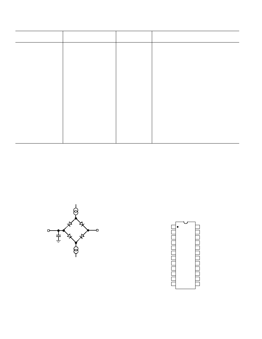
PIN CONFIGURATION
DIP AND SOIC
SCLK
MCLK IN
DGND
DV
DD
MODE
AIN1(+)
AGND
MCLK OUT
A0
SDATA
AIN1()
I
OUT
REF OUT
REF IN(+)
REF IN()
AV
DD
V
BIAS
14
1
2
24
23
5
6
7
20
19
18
3
4
22
21
8
17
9
16
10
15
11
TOP VIEW
(Not to Scale)
11
12
13
AD7710
SYNC
V
SS
DRDY
RFS
TFS
AIN2(+)
AIN2()
TO OUTPUT
PIN
+2.1V
1.6mA
200 A
100pF
Figure 1. Load Circuit for Access Time and Bus Relinquish
Time

AD7710
REV. F
7
PIN FUNCTION DESCRIPTIONS
Pin
Mnemonic
Function
1
SCLK
Serial Clock. Logic Input/Output depending on the status of the MODE pin. When MODE is high, the
device is in its self-clocking mode and the SCLK pin provides a serial clock output. This SCLK becomes
active when
RFS or TFS goes low and it goes high impedance when either RFS or TFS returns high or when
the device has completed transmission of an output word. When MODE is low, the device is in its external
clocking mode and the SCLK pin acts as an input. This input serial clock can be a continuous clock with all
data transmitted in a continuous train of pulses. Alternatively, it can be a noncontinuous clock with the
information being transmitted to the AD7710 in smaller batches of data.
2
MCLK IN
Master Clock signal for the device. This can be provided in the form of a crystal or external clock. A crystal
can be tied across the MCLK IN and MCLK OUT pins. Alternatively, the MCLK IN pin can be driven with
a CMOS compatible clock and MCLK OUT left unconnected. The clock input frequency is nominally
10 MHz.
3
MCLK OUT When the master clock for the device is a crystal, the crystal is connected between MCLK IN and MCLK
OUT.
4
A0
Address Input. With this input low, reading and writing to the device is to the control register. With this
input high, access is to either the data register or the calibration registers.
5
SYNC
Logic Input which allows for synchronization of the digital filters when using a number of AD7710s. It resets
the nodes of the digital filter.
6
MODE
Logic Input. When this pin is high, the device is in its self-clocking mode; with this pin low, the device is in
its external clocking mode.
7
AIN1(+)
Analog Input Channel 1. Positive input of the programmable gain differential analog input. The AIN1(+)
input is connected to an output current source which can be used to check that an external transducer has
burned out or gone open circuit. This output current source can be turned on/off via the control register.
8
AIN1()
Analog Input Channel 1. Negative input of the programmable gain differential analog input.
9
AIN2(+)
Analog Input Channel 2. Positive input of the programmable gain differential analog input.
10
AIN2()
Analog Input Channel 2. Negative input of the programmable gain differential analog input.
11
V
SS
Analog Negative Supply, 0 V to 5 V. Tied to AGND for single supply operation. The input voltage on
AIN1 or AIN2 should not go > 30 mV negative w.r.t. V
SS
for correct operation of the device.
12
AV
DD
Analog Positive Supply Voltage, +5 V to +10 V.
13
V
BIAS
Input Bias Voltage. This input voltage should be set such that V
BIAS
+ 0.85
×
V
REF
< AV
DD
and V
BIAS
0.85
×
V
REF
> V
SS
where V
REF
is REF IN(+) REF IN(). Ideally, this should be tied halfway between
AV
DD
, and V
SS
. Thus with AV
DD
= +5 V and V
SS
= 0 V, it can be tied to REF OUT; with AV
DD
= +5 V
and V
SS
= 5 V, it can be tied to AGND while with AV
DD
= +10 V, it can be tied to +5 V.
14
REF IN()
Reference Input. The REF IN() can lie anywhere between AV
DD
and V
SS
provided REF IN(+) is greater
than REF IN().
15
REF IN(+)
Reference Input. The reference input is differential providing that REF IN(+) is greater than REF IN().
REF IN(+) can lie anywhere between AV
DD
and V
SS
.
16
REF OUT
Reference Output. The internal +2.5 V reference is provided at this pin. This is a single ended output which
is referred to AGND. It is a buffered output which is capable of providing 1 mA to an external load.
17
I
OUT
Compensation Current Output. A 20
µ
A constant current is provided at this pin. This current can be used in
association with an external thermistor to provide cold junction compensation in thermocouple applications.
This current can be turned on or off via the control register.
18
AGND
Ground reference point for analog circuitry.

REV. F
8
AD7710
Pin
Mnemonic
Function
19
TFS
Transmit Frame Synchronization. Active low logic input used to write serial data to the device with serial data
expected after the falling edge of this pulse. In the self-clocking mode, the serial clock becomes active after
TFS goes low. In the external clocking mode, TFS must go low before the first bit of the data word is written
to the part.
20
RFS
Receive Frame Synchronization. Active low logic input used to access serial data from the device. In the
self-clocking mode, the SCLK and SDATA lines both become active after
RFS goes low. In the external
clocking mode, the SDATA line becomes active after
RFS goes low.
21
DRDY
Logic Output. A falling edge indicates that a new output word is available for transmission. The
DRDY pin
will return high upon completion of transmission of a full output word.
DRDY is also used to indicate when
the AD7710 has completed its on-chip calibration sequence.
22
SDATA
Serial Data. Input/Output with serial data being written to either the control register or the calibration regis-
ters and serial data being accessed from the control register, calibration registers or the data register.
During an output data read operation, serial data becomes active after
RFS goes low (provided DRDY is low).
During a write operation, valid serial data is expected on the rising edges of SCLK when
TFS is low. The
output data coding is natural binary for unipolar inputs and offset binary for bipolar inputs.
23
DV
DD
Digital Supply Voltage, +5 V. DV
DD
should not exceed AV
DD
by more than 0.3 V in normal operation.
24
DGND
Ground reference point for digital circuitry.
TERMINOLOGY
INTEGRAL NONLINEARITY
This is the maximum deviation of any code from a straight line
passing through the endpoints of the transfer function. The
endpoints of the transfer function are zero scale (not to be con-
fused with bipolar zero), a point 0.5 LSB below the first code
transition (000 . . . 000 to 000 . . . 001) and full scale, a point
0.5 LSB above the last code transition (111 . . . 110 to 111 . . .
111). The error is expressed as a percentage of full scale.
POSITIVE FULL-SCALE ERROR
Positive Full-Scale Error is the deviation of the last code transi-
tion (111 . . . 110 to 111 . . . 111) from the ideal AIN(+) voltage
(AIN() + V
REF
/GAIN 3/2 LSBs). It applies to both unipolar
and bipolar analog input ranges.
UNIPOLAR OFFSET ERROR
Unipolar Offset Error is the deviation of the first code transition
from the ideal AIN(+) voltage (AIN() + 0.5 LSB) when oper-
ating in the unipolar mode.
BIPOLAR ZERO ERROR
This is the deviation of the midscale transition (0111 . . . 111 to
1000 . . . 000) from the ideal AIN(+) voltage (AIN() 0.5 LSB)
when operating in the bipolar mode.
BIPOLAR NEGATIVE FULL-SCALE ERROR
This is the deviation of the first code transition from the ideal
AIN(+) voltage (AIN() V
REF
/GAIN + 0.5 LSB) when operat-
ing in the bipolar mode.
POSITIVE FULL-SCALE OVERRANGE
Positive Full-Scale Overrange is the amount of overhead avail-
able to handle input voltages on AIN(+) input greater than
AIN() +V
REF
/GAIN (for example, noise peaks or excess volt-
ages due to system gain errors in system calibration routines)
without introducing errors due to overloading the analog modu-
lator or to overflowing the digital filter.
NEGATIVE FULL-SCALE OVERRANGE
This is the amount of overhead available to handle voltages on
AIN(+) below AIN() V
REF
/GAIN without overloading the
analog modulator or overflowing the digital filter. Note that the
analog input will accept negative voltage peaks even in the uni-
polar mode provided that AIN(+) is greater than AIN() and
greater than V
SS
30 mV.
OFFSET CALIBRATION RANGE
In the system calibration modes, the AD7710 calibrates its offset
with respect to the analog input. The Offset Calibration Range
specification defines the range of voltages that the AD7710 can
accept and still calibrate offset accurately.
FULL-SCALE CALIBRATION RANGE
This is the range of voltages that the AD7710 can accept in the
system calibration mode and still calibrate full scale correctly.
INPUT SPAN
In system calibration schemes, two voltages applied in sequence
to the AD7710's analog input define the analog input range.
The input span specification defines the minimum and maxi-
mum input voltages from zero to full scale that the AD7710 can
accept and still calibrate gain accurately.
AD7710
REV. F
9
CONTROL REGISTER (24 BITS)
A write to the device with the A0 input low writes data to the control register. A read to the device with the A0 input low accesses the
contents of the control register. The control register is 24 bits wide and when writing to the register 24 bits of data must be written
otherwise the data will not be loaded to the control register. In other words, it is not possible to write just the first 12 bits of data into
the control register. If more than 24 clock pulses are provided before
TFS returns high, then all clock pulses after the 24th clock
pulse are ignored. Similarly, a read operation from the control register should access 24 bits of data.
MSB
MD2
MD1
MD0
G2
G1
G0
CH
PD
WL
IO
BO
B/U
FS11
FS10
FS9
FS8
FS7
FS6
FS5
FS4
FS3
FS2
FS1
FS0
LSB
Operating Mode
MD2
MD1
MD0
Operating Mode
0
0
0
Normal Mode. This is the normal mode of operation of the device whereby a read to the device with A0
high accesses data from the data register. This is the default condition of these bits after the internal
power on reset.
0
0
1
Activate Self-Calibration. This activates self-calibration on the channel selected by CH. This is a one-step
calibration sequence, and when complete, the part returns to normal mode (with MD2, MD1, MD0 of
the control register returning to 0, 0, 0). The
DRDY output indicates when this self-calibration is complete.
For this calibration type, the zero-scale calibration is done internally on shorted (zeroed) inputs and the
full-scale calibration is done internally on V
REF
.
0
1
0
Activate System Calibration. This activates system calibration on the channel selected by CH. This is a
two-step calibration sequence, with the zero-scale calibration done first on the selected input channel and
DRDY indicating when this zero-scale calibration is complete. The part returns to normal mode at the
end of this first step in the two-step sequence.
0
1
1
Activate System Calibration. This is the second step of the system calibration sequence with full-scale
calibration being performed on the selected input channel. Once again,
DRDY indicates when the full-
scale calibration is complete. When this calibration is complete, the part returns to normal mode.
1
0
0
Activate System Offset Calibration. This activates system offset calibration on the channel selected by
CH. This is a one-step calibration sequence and, when complete, the part returns to normal mode with
DRDY indicating when this system offset calibration is complete. For this calibration type, the zero-scale
calibration is done on the selected input channel and the full-scale calibration is done internally on V
REF
.
1
0
1
Activate Background Calibration. This activates background calibration on the channel selected by CH. If
the background calibration mode is on, then the AD7710 provides continuous self-calibration of the
reference and shorted (zeroed) inputs. This calibration takes place as part of the conversion sequence,
extending the conversion time and reducing the word rate by a factor of six. Its major advantage is that
the user does not have to worry about recalibrating the device when there is a change in the ambient
temperature. In this mode, the shorted (zeroed) inputs and V
REF
, as well as the analog input voltage, are
continuously monitored and the calibration registers of the device are automatically updated.
1
1
0
Read/Write Zero-Scale Calibration Coefficients. A read to the device with A0 high accesses the contents
of the zero-scale calibration coefficients of the channel selected by CH. A write to the device with A0 high
writes data to the zero-scale calibration coefficients of the channel selected by CH. The word length for
reading and writing these coefficients is 24 bits, regardless of the status of the WL bit of the control
register. Therefore, when writing to the calibration register 24 bits of data must be written, otherwise the
new data will not be transferred to the calibration register.
1
1
1
Read/Write Full-Scale Calibration Coefficients. A read to the device with A0 high accesses the contents of
the full-scale calibration coefficients of the channel selected by CH. A write to the device with A0 high
writes data to the full-scale calibration coefficients of the channel selected by CH. The word length for
reading and writing these coefficients is 24 bits, regardless of the status of the WL bit of the control
register. Therefore, when writing to the calibration register 24 bits of data must be written, otherwise the
new data will not be transferred to the calibration register.

REV. F
10
AD7710
PGA GAIN
G2
G1
G0
Gain
0
0
0
1
(Default Condition After the Internal Power-On Reset)
0
0
1
2
0
1
0
4
0
1
1
8
1
0
0
16
1
0
1
32
1
1
0
64
1
1
1
128
Channel Selection
CH
Channel
0
AIN1
(Default Condition After the Internal Power-On Reset)
1
AIN2
Power-Down
PD
0
Normal Operation
(Default Condition After the Internal Power-On Reset)
1
Power-Down
Word Length
WL
Output Word Length
0
16-Bit
(Default Condition After Internal Power-On Reset)
1
24-Bit
Output Compensation Current
IO
0
Off
(Default Condition After Internal Power-On Reset)
1
On
Burn-Out Current
BO
0
Off
(Default Condition After Internal Power-On Reset)
1
On
Bipolar/Unipolar Selection (Both Inputs)
B/U
0
Bipolar
(Default Condition After Internal Power-On Reset)
1
Unipolar
Filter Selection (FS11FS0)
The on-chip digital filter provides a Sinc
3
(or (Sinx/x)
3
) filter response. The 12 bits of data programmed into these bits determine the
filter cutoff frequency, the position of the first notch of the filter and the data rate for the part. In association with the gain selection,
it also determines the output noise (and hence the effective resolution) of the device.
The first notch of the filter occurs at a frequency determined by the relationship: filter first notch frequency = (f
CLK
IN
/512)/code
where code is the decimal equivalent of the code in bits FS0 to FS11 and is in the range 19 to 2,000. With the nominal f
CLK IN
of
10 MHz, this results in a first notch frequency range from 9.76 Hz to 1.028 kHz. To ensure correct operation of the AD7710, the
value of the code loaded to these bits must be within this range. Failure to do this will result in unspecified operation of the device.
Changing the filter notch frequency, as well as the selected gain, impacts resolution. Tables I and II and Figure 2 show the effect of
the filter notch frequency and gain on the effective resolution of the AD7710. The output data rate (or effective conversion time) for
the device is equal to the frequency selected for the first notch of the filter. For example, if the first notch of the filter is selected at
50 Hz, then a new word is available at a 50 Hz rate or every 20 ms. If the first notch is at 1 kHz, a new word is available every 1 ms.
The settling time of the filter to a full-scale step input change is worst case 4
×
1/(output data rate). This settling time is to 100% of
the final value. For example, with the first filter notch at 50 Hz, the settling time of the filter to a full-scale step input change is
80 ms max. If the first notch is at 1 kHz, the settling time of the filter to a full-scale input step is 4 ms max. This settling time can be
reduced to 3
×
l/(output data rate) by synchronizing the step input change to a reset of the digital filter. In other words, if the step
input takes place with
SYNC low, the settling time will be 3
×
l/(output data rate). If a change of channels takes place, the settling
time is 3
×
l/(output data rate) regardless of the
SYNC input.
The 3 dB frequency is determined by the programmed first notch frequency according to the relationship: filter 3 dB frequency
= 0.262
×
first notch frequency.
AD7710
REV. F
11
Tables I and II show the output rms noise for some typical notch and 3 dB frequencies. The numbers given are for the bipolar
input ranges with a V
REF
of +2.5 V. These numbers are typical and are generated with an analog input voltage of 0 V. The output
noise from the part comes from two sources. First, there is the electrical noise in the semiconductor devices used in the implementa-
tion of the modulator (device noise). Secondly, when the analog input signal is converted into the digital domain, quantization noise
is added. The device noise is at a low level and is largely independent of frequency. The quantization noise starts at an even lower
level but rises rapidly with increasing frequency to become the dominant noise source. Consequently, lower filter notch settings
(below 60 Hz approximately) tend to be device noise dominated while higher notch settings are dominated by quantization noise.
Changing the filter notch and cutoff frequency in the quantization noise dominated region results in a more dramatic improvement
in noise performance than it does in the device noise dominated region as shown in Table I. Furthermore, quantization noise is
added after the PGA, so effective resolution is independent of gain for the higher filter notch frequencies. Meanwhile, device noise is
added in the PGA and, therefore, effective resolution suffers a little at high gains for lower notch frequencies.
At the lower filter notch settings (below 60 Hz), the no missing codes performance of the device is at the 24-bit level. At the higher
settings, more codes will be missed until at 1 kHz notch setting, no missing codes performance is only guaranteed to the 12-bit level.
However, since the effective resolution of the part is 10.5 bits for this filter notch setting, this no missing codes performance should
be more than adequate for all applications.
The effective resolution of the device is defined as the ratio of the output rms noise to the input full scale. This does not remain
constant with increasing gain or with increasing bandwidth. Table II shows the same table as Table I except that the output is now
expressed in terms of effective resolution (the magnitude of the rms noise with respect to 2
×
V
REF
/GAIN, i.e., the input full scale). It
is possible to do post filtering on the device to improve the output data rate for a given 3 dB frequency and also to further reduce
the output noise (see Digital Filtering section).
Table I. Output Noise vs. Gain and First Notch Frequency
First Notch of
Typical Output RMS Noise ( V)
Filter & O/P
3 dB
Gain of
Gain of
Gain of
Gain of
Gain of
Gain of
Gain of
Gain of
Data Rate
1
Frequency
1
2
4
8
16
32
64
128
10 Hz
2
2.62 Hz
1.0
0.78
0.48
0.33
0.25
0.25
0.25
0.25
25 Hz
2
6.55 Hz
1.8
1.1
0.63
0.5
0.44
0.41
0.38
0.38
30 Hz
2
7.86 Hz
2.5
1.31
0.84
0.57
0.46
0.43
0.4
0.4
50 Hz
2
13.1 Hz
4.33
2.06
1.2
0.64
0.54
0.46
0.46
0.46
60 Hz
2
15.72 Hz
5.28
2.36
1.33
0.87
0.63
0.62
0.6
0.56
100 Hz
3
26.2 Hz
13
6.4
3.7
1.8
1.1
0.9
0.65
0.65
250 Hz
3
65.5 Hz
130
75
25
12
7.5
4
2.7
1.7
500 Hz
3
131 Hz
0.6
×
10
3
0.26
×
10
3
140
70
35
25
15
8
1 kHz
3
262 Hz
3.1
×
10
3
1.6
×
10
3
0.7
×
10
3
0.29
×
10
3
180
120
70
40
NOTES
1
The default condition (after the internal power-on reset) for the first notch of filter is 60 Hz.
2
For these filter notch frequencies, the output rms noise is primarily dominated by device noise and as a result is independent of the value of the reference voltage.
Therefore, increasing the reference voltage will give an increase in the effective resolution of the device (i.e., the ratio of the rms noise to the input full scale is
increased since the output rms noise remains constant as the input full scale increases).
3
For these filter notch frequencies, the output rms noise is dominated by quantization noise and as a result is proportional to the value of the reference voltage.
Table II. Effective Resolution vs. Gain and First Notch Frequency
First Notch of
Effective Resolution
1
(Bits)
Filter & O/P
3 dB
Gain of
Gain of
Gain of
Gain of
Gain of
Gain of
Gain of
Gain of
Data Rate
Frequency
1
2
4
8
16
32
64
128
10 Hz
2.62 Hz
22.5
21.5
21.5
21
20.5
19.5
18.5
17.5
25 Hz
6.55 Hz
21.5
21
21
20
19.5
18.5
17.5
16.5
30 Hz
7.86 Hz
21
21
20.5
20
19.5
18.5
17.5
16.5
50 Hz
13.1 Hz
20
20
20
19.5
19
18.5
17.5
16.5
60 Hz
15.72 Hz
20
20
20
19.5
19
18
17
16
100 Hz
26.2 Hz
18.5
18.5
18.5
18.5
18
17.5
17
16
250 Hz
65.5 Hz
15
15
15.5
15.5
15.5
15.5
15
14.5
500 Hz
131 Hz
13
13
13
13
13
12.5
12.5
12.5
1 kHz
262 Hz
10.5
10.5
11
11
11
10.5
10
10
NOTE
1
Effective resolution is defined as the magnitude of the output rms noise with respect to the input full scale (i.e., 2
×
V
REF
/GAIN). The above table applies for a V
REF
of +2.5 V and resolution numbers are rounded to the nearest 0.5 LSB.
REV. F
12
AD7710
1k
10
0.1
10
1k
10k
100
1
100
NOTCH FREQUENCY Hz
OUTPUT NOISE
V
GAIN OF 16
GAIN OF 32
GAIN OF 64
GAIN OF 128
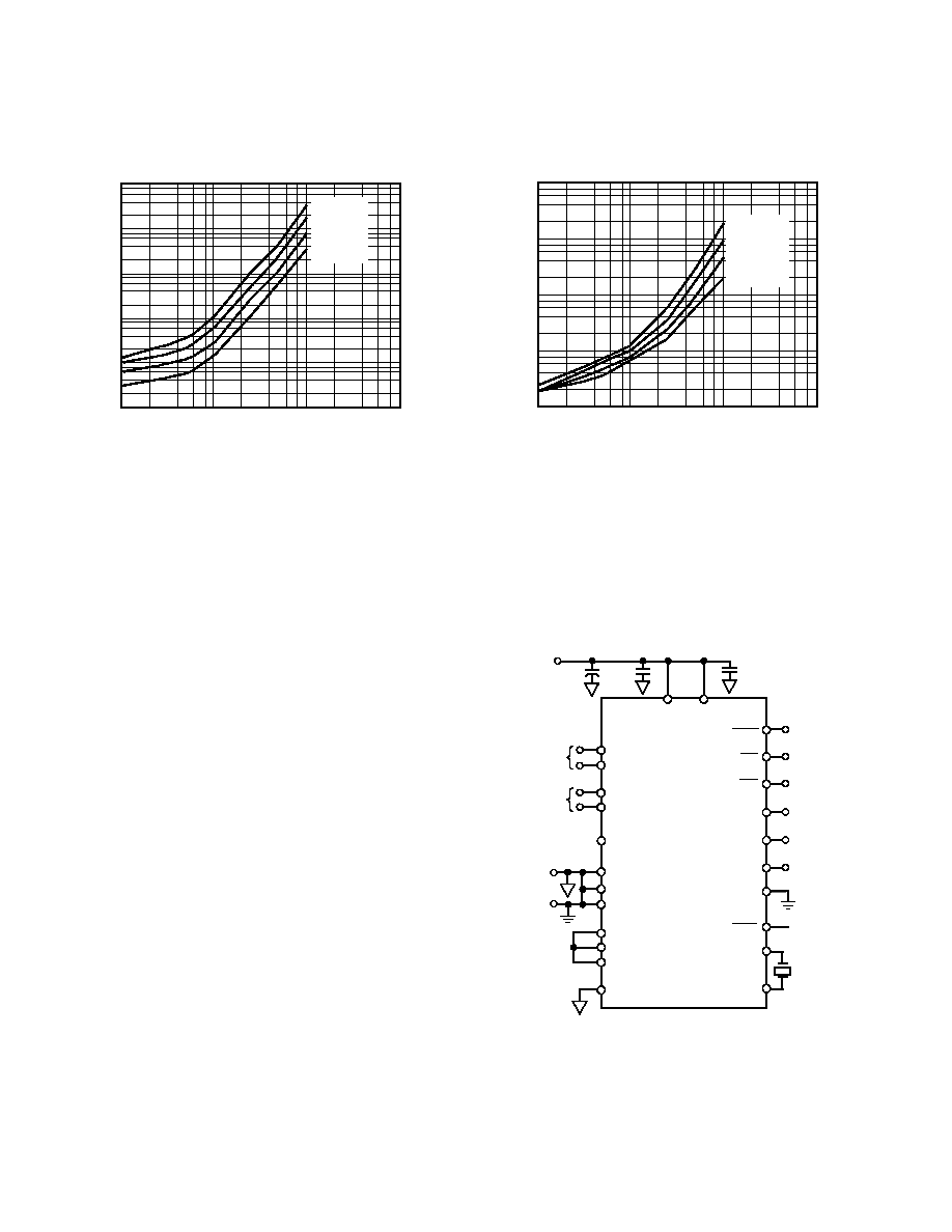
Figure 2b. Plot of Output Noise vs. Gain and Notch
Frequency (Gains of 16 to 128)
The basic connection diagram for the part is shown in Figure 3.
This shows the AD7710 in the external clocking mode with
both the AV
DD
and DV
DD
pins of the AD7710 being driven
from the analog +5 V supply. Some applications will have
separate supplies for both AV
DD
and DV
DD
, and in some of
these cases, the analog supply will exceed the +5 V digital sup-
ply (see Power Supplies and Grounding section).
REF IN(+)
REF OUT
AIN1(+)
AIN1()
AIN2(+)
AGND
DGND
MCLK IN
MCLK OUT
MODE
SCLK
SDATA
DRDY
TFS
RFS
REF IN()
V
BIAS
SYNC
A0
DIFFERENTIAL
ANALOG INPUT
ANALOG
GROUND
DIGITAL
GROUND
DATA
READY
TRANSMIT
(WRITE)
RECEIVE
(READ)
SERIAL
DATA
SERIAL
CLOCK
ADDRESS
INPUT
+5V
AD7710
10 F
0.1 F
0.1 F
ANALOG
+5V SUPPLY
AV
DD
DV
DD
V
SS
I
OUT
AIN2()
DIFFERENTIAL
ANALOG INPUT
Figure 3. Basic Connection Diagram
Figure 2 gives similar information to that outlined in Table I. In this plot, the output rms noise is shown for the full range of avail-
able cutoffs frequencies rather than for some typical cutoff frequencies as in Tables I and II. The numbers given in these plots are
typical values at 25
°
C.
10k
100
0.1
10
1k
10k
1k
10
1
100
GAIN OF 1
GAIN OF 2
GAIN OF 4
GAIN OF 8
NOTCH FREQUENCY Hz
OUTPUT NOISE
V
Figure 2a. Plot of Output Noise vs. Gain and Notch
Frequency (Gains of 1 to 8)
CIRCUIT DESCRIPTION
The AD7710 is a sigma-delta A/D converter with on-chip digital
filtering, intended for the measurement of wide dynamic range,
low frequency signals such as those in weigh scale, industrial
control or process control applications. It contains a sigma-delta
(or charge balancing) ADC, a calibration microcontroller with
on-chip static RAM, a clock oscillator, a digital filter and a bi-
directional serial communications port.
The part contains two programmable gain differential analog
input channels. The gain range is from 1 to 128 allowing the
part to accept unipolar signals of between 0 mV to +20 mV and
0 V to +2.5 V or bipolar signals in the range from
±
20 mV to
±
2.5 V when the reference input voltage equals +2.5 V. The
input signal to the selected analog input channel is continuously
sampled at a rate determined by the frequency of the master
clock, MCLK IN, and the selected gain (see Table III). A
charge-balancing A/D converter (Sigma-Delta Modulator) con-
verts the sampled signal into a digital pulse train whose duty
cycle contains the digital information. The programmable gain
function on the analog input is also incorporated in this sigma-
delta modulator with the input sampling frequency being modi-
fied to give the higher gains. A sinc
3
digital low-pass filter
processes the output of the sigma-delta modulator and updates
the output register at a rate determined by the first notch fre-
quency of this filter. The output data can be read from the serial
port randomly or periodically at any rate up to the output regis-
ter update rate. The first notch of this digital filter (and hence its
3 dB frequency) can be programmed via an on-chip control
register. The programmable range for this first notch frequency
is from 9.76 Hz to 1.028 kHz, giving a programmable range for
the 3 dB frequency of 2.58 Hz to 269 Hz.
AD7710
REV. F
13
In operation, the analog signal sample is fed to the subtracter,
along with the output of the 1-bit DAC. The filtered difference
signal is fed to the comparator, whose output samples the dif-
ference signal at a frequency many times that of the analog
signal sampling frequency (oversampling).
Oversampling is fundamental to the operation of sigma-delta
ADCs. Using the quantization noise formula for an ADC:
SNR = (6.02
×
number of bits + 1.76) dB,
a 1-bit ADC or comparator yields an SNR of 7.78 dB.
The AD7710 samples the input signal at a frequency of 39 kHz or
greater (see Table III). As a result, the quantization noise is
spread over a much wider frequency than that of the band of
interest. The noise in the band of interest is reduced still further
by analog filtering in the modulator loop, which shapes the
quantization noise spectrum to move most of the noise energy to
frequencies outside the bandwidth of interest. The noise perfor-
mance is thus improved from this 1-bit level to the performance
outlined in Tables I and II and in Figure 2.
The output of the comparator provides the digital input for the
1-bit DAC, so that the system functions as a negative feedback
loop that tries to minimize the difference signal. The digital data
that represents the analog input voltage is contained in the duty
cycle of the pulse train appearing at the output of the compara-
tor. It can be retrieved as a parallel binary data word using a
digital filter.
Sigma-delta ADCs are generally described by the order of the
analog low-pass filter. A simple example of a first order sigma-
delta ADC is shown in Figure 5. This contains only a first order
low-pass filter or integrator. It also illustrates the derivation of
the alternative name for these devices: Charge Balancing ADCs.
+FS
FS
DAC
DIFFERENTIAL
AMPLIFIER
COMPARATOR
INTEGRATOR
V
IN
Figure 5. Basic Charge-Balancing ADC
It consists of a differential amplifier (whose output is the differ-
ence between the analog input and the output of a 1-bit DAC),
an integrator and a comparator. The term, charge-balancing,
comes from the fact that this system is a negative feedback loop
that tries to keep the net charge on the integrator capacitor at
zero, by balancing charge injected by the input voltage with
charge injected by the 1-bit DAC. When the analog input is
zero, the only contribution to the integrator output comes from
the 1-bit DAC. For the net charge on the integrator capacitor to
be zero, the DAC output must spend half its time at +FS and
half its time at FS. Assuming ideal components, the duty cycle
of the comparator will be 50%.
When a positive analog input is applied, the output of the 1-bit
DAC must spend a larger proportion of the time at +FS, so the
duty cycle of the comparator increases. When a negative input
voltage is applied, the duty cycle decreases.
The AD7710 uses a second order sigma-delta modulator and a
digital filter that provides a rolling average of the sampled out-
put. After power-up, or if there is a step change in the input
voltage, there is a settling time that must elapse before valid
data is obtained.
The AD7710 provides a number of calibration options which
can be programmed via the on-chip control register. A calibra-
tion cycle may be initiated at any time by writing to this control
register. The part can perform self-calibration using the on-chip
calibration microcontroller and SRAM to store calibration
parameters. Other system components may also be included in
the calibration loop to remove offset and gain errors in the input
channel using the system calibration mode. Another option is a
background calibration mode where the part continuously per-
forms self-calibration and updates the calibration coefficients.
Once the part is in this mode, the user does not have to worry
about issuing periodic calibration commands to the device or
asking the device to recalibrate when there is a change in the
ambient temperature or power supply voltage.
The AD7710 gives the user access to the on-chip calibration
registers allowing the microprocessor to read the device's cali-
bration coefficients and also to write its own calibration coeffi-
cients to the part from prestored values in E
2
PROM. This gives
the microprocessor much greater control over the AD7710's
calibration procedure. It also means that the user can verify that
the device has performed its calibration correctly by comparing the
coefficients after calibration with prestored values in E
2
PROM.
The AD7710 can be operated in single supply systems provided
that the analog input voltage does not go more negative than
30 mV. For larger bipolar signals, a V
SS
of 5 V is required by
the part. For battery operation, the AD7710 also offers a soft-
ware-programmable standby mode that reduces idle power
consumption to typically 7 mW.
THEORY OF OPERATION
The general block diagram of a sigma-delta ADC is shown in
Figure 4. It contains the following elements:
1. A sample-hold amplifier.
2. A differential amplifier or subtracter.
3. An analog low-pass filter.
4. A 1-bit A/D converter (comparator).
5. A 1-bit DAC.
6. A digital low-pass filter.
S/H AMP
COMPARATOR
DIGITAL DATA
DIGITAL
FILTER
ANALOG
LOW-PASS
FILTER
DAC
Figure 4. General Sigma-Delta ADC
REV. F
14
AD7710
Input Sample Rate
The modulator sample frequency for the device remains at
f
CLK IN
/512 (19.5 kHz @ f
CLK IN
= 10 MHz) regardless of the
selected gain. However, gains greater than
×
1 are achieved by a
combination of multiple input samples per modulator cycle and
a scaling of the ratio of reference capacitor to input capacitor.
As a result of the multiple sampling, the input sample rate of
the device varies with the selected gain (see Table III). The
effective input impedance is 1/C
×
f
S
where C is the input sam-
pling capacitance and f
S
is the input sample rate.
Table III. Input Sampling Frequency vs. Gain
Gain
Input Sampling Frequency (f
S
)
1
f
CLK IN
/256 (39 kHz @ f
CLK IN
= 10 MHz)
2
2
×
f
CLK IN
/256 (78 kHz @ f
CLK IN
= 10 MHz)
4
4
×
f
CLK IN
/256 (156 kHz @ f
CLK IN
= 10 MHz)
8
8
×
f
CLK IN
/256 (312 kHz @ f
CLK IN
= 10 MHz)
16
8
×
f
CLK IN
/256 (312 kHz @ f
CLK IN
= 10 MHz)
32
8
×
f
CLK IN
/256 (312 kHz @ f
CLK IN
= 10 MHz)
64
8
×
f
CLK IN
/256 (312 kHz @ f
CLK IN
= 10 MHz)
128
8
×
f
CLK IN
/256 (312 kHz @ f
CLK IN
= 10 MHz)
DIGITAL FILTERING
The AD7710's digital filter behaves like a similar analog filter,
with a few minor differences.
First, since digital filtering occurs after the A-to-D conversion
process, it can remove noise injected during the conversion
process. Analog filtering cannot do this.
On the other hand, analog filtering can remove noise super-
imposed on the analog signal before it reaches the ADC. Digital
filtering cannot do this and noise peaks riding on signals near
full scale have the potential to saturate the analog modulator
and digital filter, even though the average value of the signal is
within limits. To alleviate this problem, the AD7710 has over-
range headroom built into the sigma-delta modulator and digital
filter which allows overrange excursions of 5% above the analog
input range. If noise signals are larger than this, consideration
should be given to analog input filtering, or to reducing the
input channel voltage so that its full scale is half that of the
analog input channel full scale. This will provide an overrange
capability greater than 100% at the expense of reducing the
dynamic range by 1 bit (50%).
Filter Characteristics
The cutoff frequency of the digital filter is determined by the
value loaded to bits FS0 to FS11 in the control register. At the
maximum clock frequency of 10 MHz, the minimum cutoff
frequency of the filter is 2.58 Hz while the maximum program-
mable cutoff frequency is 269 Hz.
Figure 6 shows the filter frequency response for a cutoff fre-
quency of 2.62 Hz which corresponds to a first filter notch
frequency of 10 Hz. This is a (sinx/x)
3
response (also called
sinc
3
) that provides >100 dB of 50 Hz and 60 Hz rejection.
Programming a different cutoff frequency via FS0FS11 does
not alter the profile of the filter response, it changes the frequency
of the notches as outlined in the Control Register section.
GAIN dB
FREQUENCY Hz
0
240
0
70
10
20
30
40
50
60
40
80
120
160
200
20
60
100
140
180
220
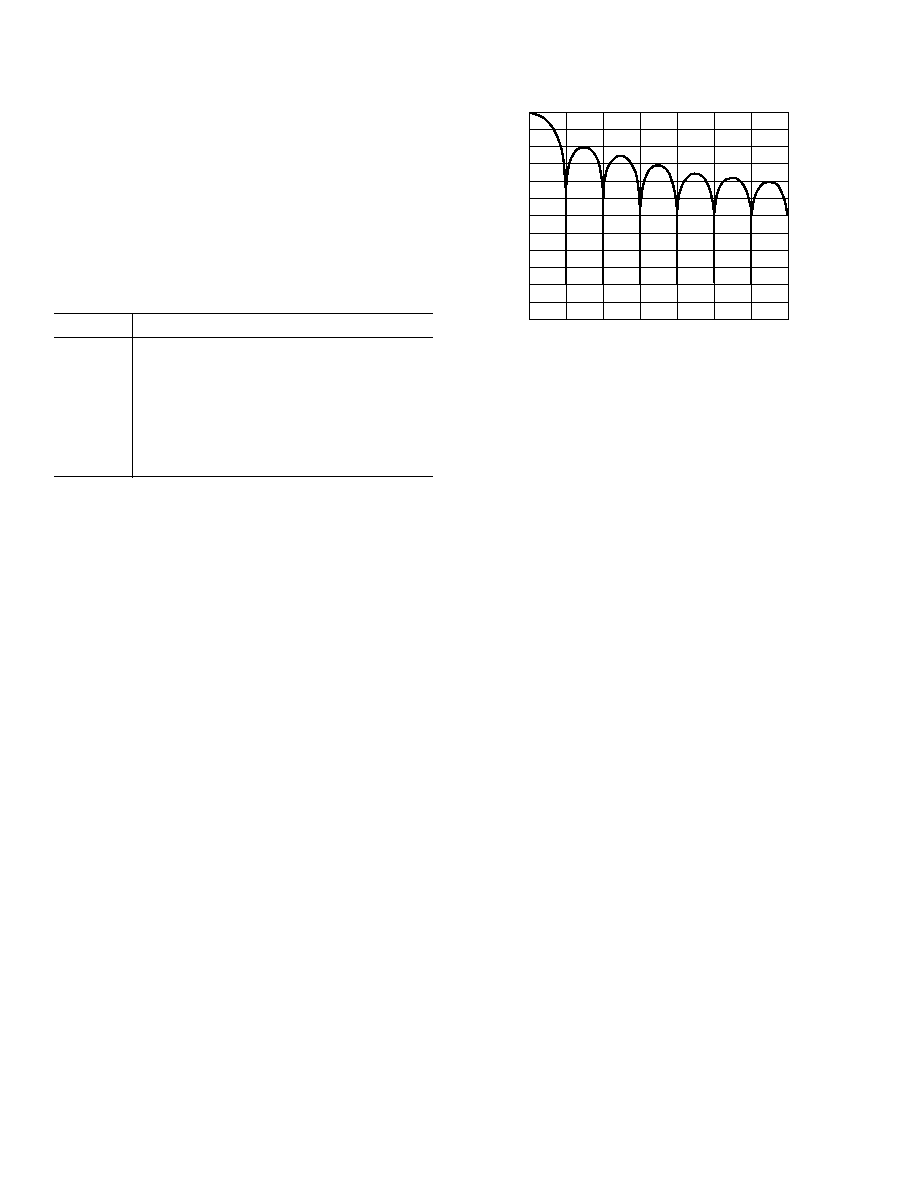
Figure 6. Frequency Response of AD7710 Filter
Since the AD7710 contains this on-chip, low-pass filtering,
there is a settling time associated with step function inputs, and
data on the output will be invalid after a step change until the
settling time has elapsed. The settling time depends upon the
notch frequency chosen for the filter. The output data rate
equates to this filter notch frequency and the settling time of the
filter to a full-scale step input is four times the output data
period. In applications using both input channels, the settling
time of the filter must be allowed to elapse before data from the
second channel is accessed.
Post Filtering
The on-chip modulator provides samples at a 19.5 kHz output
rate. The on-chip digital filter decimates these samples to pro-
vide data at an output rate which corresponds to the pro-
grammed first notch frequency of the filter. Since the output
data rate exceeds the Nyquist criterion, the output rate for a
given bandwidth will satisfy most application requirements.
However, there may be some applications which require a
higher data rate for a given bandwidth and noise performance.
Applications which need this higher data rate will require some
post filtering following the digital filter of the AD7710.
For example, if the required bandwidth is 7.86 Hz but the
required update rate is 100 Hz, the data can be taken from the
AD7710 at the 100 Hz rate giving a 3 dB bandwidth of
26.2 Hz. Post filtering can be applied to this to reduce the
bandwidth and output noise, to the 7.86 Hz bandwidth level,
while maintaining an output rate of 100 Hz.
Post filtering can also be used to reduce the output noise from
the device for bandwidths below 2.62 Hz. At a gain of 128, the
output rms noise is 250 nV. This is essentially device noise or
white noise, and since the input is chopped, the noise has a flat
frequency response. By reducing the bandwidth below 2.62 Hz,
the noise in the resultant passband can be reduced. A reduction
in bandwidth by a factor of two results in a
2 reduction in the
output rms noise. This additional filtering will result in a longer
settling time.
AD7710
REV. F
15
Antialias Considerations
The digital filter does not provide any rejection at integer mul-
tiples of the modulator sample frequency (n
×
19.5 kHz, where
n = 1, 2, 3 . . . ). This means that there are frequency bands,
±
f
3 dB
wide (f
3 dB
is cutoff frequency selected by FS0 to FS11)
where noise passes unattenuated to the output. However, due to
the AD7710's high oversampling ratio, these bands occupy only
a small fraction of the spectrum and most broadband noise is
filtered. In any case, because of the high oversampling ratio a
simple, RC, single pole filter is generally sufficient to attenuate
the signals in these bands on the analog input and thus provide
adequate antialiasing filtering.
If passive components are placed in front of the AD7710, care
must be taken to ensure that the source impedance is low enough
so as not to introduce gain errors in the system. The dc input
impedance for the AD7710 is over 1 G
. The input appears as
a dynamic load which varies with the clock frequency and with
the selected gain (see Figure 7). The input sample rate, as
shown in Table III, determines the time allowed for the analog
input capacitor, C
IN
, to be charged. External impedances result
in a longer charge time for this capacitor and this may result
in gain errors being introduced on the analog inputs. Table IV
shows the allowable external resistance/capacitance values such
that no gain error to the 16-bit level is introduced while Table V
shows the allowable external resistance/capacitance values such
that no gain error to the 20-bit level is introduced. Both inputs
of the differential input channels look into similar input circuitry.
R
INT
7k TYP
C
INT
11.5pF TYP
V
BIAS
AIN
SWITCHING FREQ DEPENDS ON
f
CLKIN
AND SELECTED GAIN
HIGH
IMPEDANCE
>1G
AD7710
Figure 7. Analog Input Impedance
Table IV. Typical External Series Resistance That Will Not
Introduce 16-Bit Gain Error
External Capacitance (pF)
Gain
0
50
100
500
1000
5000
1
184 k
45.3 k
27.1 k
7.3 k
4.1 k
1.1 k
2
88.6 k
22.1 k
13.2 k
3.6 k
2.0 k
560
4
41.4 k
10.6 k
6.3 k
1.7 k
970
270
8128
17.6 k
4.8 k
2.9 k
790
440
120
Table V. Typical External Series Resistance That Will Not
Introduce 20-Bit Gain Error
External Capacitance (pF)
Gain
0
50
100
500
1000
5000
1
145 k
34.5 k
20.4 k
5.2 k
2.8 k
700
2
70.5 k
16.9 k
10 k
2.5 k
1.4 k
350
4
31.8 k
8.0 k
4.8 k
1.2 k
670
170
8128
13.4 k
3.6 k
2.2 k
550
300
80
The numbers in the above tables assume a full-scale change on
the analog input. In any case, the error introduced due to longer
charging times is a gain error which can be removed using the
system calibration capabilities of the AD7710 provided that the
resultant span is within the span limits of the system calibration
techniques for the AD7710.
ANALOG INPUT FUNCTIONS
Analog Input Ranges
Both analog inputs are differential, programmable gain, input
channels which can handle either unipolar or bipolar input
signals. The common-mode range of these inputs is from V
SS
to
AV
DD
, provided that the absolute value of the analog input
voltage lies between V
SS
30 mV and AV
DD
+30 mV.
The dc input leakage current is 10 pA maximum at 25
°
C
(
±
1 nA over temperature). This results in a dc offset voltage
developed across the source impedance. However, this dc offset
effect can be compensated for by a combination of the differen-
tial input capability of the part and its system calibration mode.
Burnout Current
The AIN1(+) input of the AD7710 contains a 4.5
µ
A current
source which can be turned on/off via the control register. This
current source can be used in checking that a transducer has not
burned out or gone open circuit before attempting to take mea-
surements on that channel. If the current is turned on and
allowed flow into the transducer and a measurement of the
input voltage on the AIN1 input is taken, it can indicate that the
transducer has burned out or gone open circuit. For normal
operation, this burnout current is turned off by writing a 0 to
the BO bit in the control register.
Output Compensation Current
The AD7710 also contains a feature which can enable the user
to implement cold junction compensation in thermocouple
applications. This can be achieved using the output compensa-
tion current from the I
OUT
pin of the device. Once again, this
current can be turned on/off via the control register. Writing a 1
to the IO bit of the control register enables this compensation
current.
The compensation current provides a 20
µ
A constant current
source which can be used in association with a thermistor or a
diode to provide cold junction compensation. A common
method of generating cold junction compensation is to use a
temperature dependent current flowing through a fixed resistor
to provide a voltage that is equal to the voltage developed across
the cold junction at any temperature in the expected ambient
range. In this case, the temperature coefficient of the compensa-
tion current is so low compared with the temperature coefficient
of the thermistor that it can be considered constant with tem-
perature. The temperature variation is then provided by the
variation of the thermistor's resistance with temperature.
Normally, the cold junction compensation will be implemented
by applying the compensation voltage to the second input chan-
nel of the AD7710. Periodic conversion of this channel gives the
user a voltage which corresponds to the cold junction compen-
sation voltage. This can be used to implement cold junction
compensation in software with the result from the thermocouple
input being adjusted according to the result in the compensation
channel. Alternatively, the voltage can be subtracted from the
input voltage in an analog fashion, thereby using only one chan-
nel of the AD7710.

REV. F
16
AD7710
Bipolar/Unipolar Inputs
The two analog inputs on the AD7710 can accept either unipo-
lar or bipolar input voltage ranges. Bipolar or unipolar options
are chosen by programming the B/U bit of the control register.
This programs both channels for either unipolar or bipolar
operation. Programming the part for either unipolar or bipolar
operation does not change any of the input signal conditioning;
it simply changes the data output coding. The data coding is
binary for unipolar inputs and offset binary for bipolar inputs.
The input channels are differential and, as a result, the voltage
to which the unipolar and bipolar signals are referenced is the
voltage on the AIN() input. For example, if AIN() is +1.25 V
and the AD7710 is configured for unipolar operation with a
gain of 1 and a V
REF
of +2.5 V, the input voltage range on the
AIN(+) input is +1.25 V to +3.75 V. If AIN() is +1.25 V and
the AD7710 is configured for bipolar mode with a gain of 1 and
a V
REF
of +2.5 V, the analog input range on the AIN(+) input is
1.25 V to +3.75 V.
REFERENCE INPUT/OUTPUT
The AD7710 contains a temperature compensated +2.5 V refer-
ence which has an initial tolerance of
±
1%. This reference volt-
age is provided at the REF OUT pin and it can be used as the
reference voltage for the part by connecting the REF OUT pin
to the REF IN(+) pin. This REF OUT pin is a single-ended
output, referenced to AGND, which is capable of providing up
to 1 mA to an external load. In applications where REF OUT is
connected to REF IN(+), REF IN() should be tied to AGND
to provide the nominal +2.5 V reference for the AD7710.
The reference inputs of the AD7710 REF IN(+) and REF IN(),
provide a differential reference input capability. The common-
mode range for these differential inputs is from V
SS
to AV
DD
.
The nominal differential voltage, V
REF
(REF IN(+)REF IN()),
is +2.5 V for specified operation, but the reference voltage can
go to +5 V with no degradation in performance provided that
the absolute value of REF IN(+) and REF IN() does not ex-
ceed its AV
DD
and V
SS
limits and the V
BIAS
input voltage range
limits are obeyed. The part is also functional with V
REF
voltage
down to 1 V but with degraded performance as the output noise
will, in terms of LSB size, be larger. REF IN(+) must always be
greater than REF IN() for correct operation of the AD7710.
Both reference inputs provide a high impedance, dynamic load
similar to the analog inputs. The maximum dc input leakage
current is 10 pA (
±
1 nA over temperature) and source resis-
tance may result in gain errors on the part. The reference inputs
look like the analog input (see Figure 7). In this case, R
INT
is
5 k
typ and C
INT
varies with gain. The input sample rate is
f
CLK IN
/256 and does not vary with gain. For gains of 1 to 8 C
INT
is 20 pF; for a gain of 16 it is 10 pF; for a gain of 32 it is 5 pF;
for a gain of 64 it is 2.5 pF; and for a gain of 128 it is 1.25 pF.
The digital filter of the AD7710 removes noise from the refer-
ence input just as it does with the analog input, and the same
limitations apply regarding lack of noise rejection at integer
multiples of the sampling frequency. The output noise perfor-
mance outlined in Tables I and II assumes a clean reference. If
the reference noise in the bandwidth of interest is excessive, it
can degrade the performance of the AD7710. Using the on-chip
reference as the reference source for the part (i.e., connecting
REF OUT to REF IN) results in somewhat degraded output
noise performance from the AD7710 for portions of the noise
table that are dominated by the device noise. The on-chip refer-
ence noise effect is eliminated in ratiometric applications where
the reference is used to provide the excitation voltage for the
analog front end. The connection scheme, shown in Figure 8, is
recommended when using the on-chip reference. Recommended
reference voltage sources for the AD7710 include the AD580
and AD680 2.5 V references.
REF OUT
REF IN (+)
AD7710
REF IN ()
Figure 8. REF OUT/REF IN Connection
V
BIAS
Input
The V
BIAS
input determine at what voltage the internal analog
circuitry is biased. It essentially provides the return path for
analog currents flowing in the modulator and, as such, it should
be driven from a low impedance point to minimize errors.
For maximum internal headroom, the V
BIAS
voltage should be
set halfway between AV
DD
and V
SS
. The difference between
AV
DD
and (V
BIAS
+ 0.85
×
V
REF
) determines the amount of
headroom the circuit has at the upper end, while the difference
between V
SS
and (V
BIAS
0.85
×
V
REF
) determines the amount
of headroom the circuit has at the lower end. Care should be
taken in choosing a V
BIAS
voltage to ensure that it stays within
prescribed limits. For single +5 V operation, the selected V
BIAS
voltage must ensure that V
BIAS
±
0.85
×
V
REF
does not exceed
AV
DD
or V
SS
or that the V
BIAS
voltage itself is greater than V
SS
+ 2.1 V and less than AV
DD
2.1 V. For single +10 V operation
or dual
±
5 V operation, the selected V
BIAS
voltage must ensure
that V
BIAS
±
0.85
×
V
REF
does not exceed AV
DD
or V
SS
or that
the V
BIAS
voltage itself is greater than V
SS
+ 3 V or less than
AV
DD
3 V. For example, with AV
DD
= +4.75 V, V
SS
= 0 V
and V
REF
= +2.5 V, the allowable range for the V
BIAS
voltage is
+2.125 V to +2.625 V. With AV
DD
= +9.5 V, V
SS
= 0 V and
V
REF
= +5 V, the range for V
BIAS
is +4.25 V to +5.25 V. With
AV
DD
= +4.75 V, V
SS
= 4.75 V and V
REF
= +2.5 V, the V
BIAS
range is 2.625 V to +2.625 V.
The V
BIAS
voltage does have an effect on the AV
DD
power sup-
ply rejection performance of the AD7710. If the V
BIAS
voltage
tracks the AV
DD
supply, it improves the power supply rejection
from the AV
DD
supply line from 80 dB to 95 dB. Using an
external Zener diode, connected between the AV
DD
line and
V
BIAS
, as the source for the V
BIAS
voltage gives the improvement
in AV
DD
power supply rejection performance.

AD7710
REV. F
17
USING THE AD7710
SYSTEM DESIGN CONSIDERATIONS
The AD7710 operates differently from successive approxima-
tion ADCs or integrating ADCs. Since it samples the signal
continuously, like a tracking ADC, there is no need for a start
convert command. The output register is updated at a rate
determined by the first notch of the filter and the output can be
read at any time, either synchronously or asynchronously.
Clocking
The AD7710 requires a master clock input, which may be an
external TTL/CMOS compatible clock signal applied to the
MCLK IN pin with the MCLK OUT pin left unconnected.
Alternatively, a crystal of the correct frequency can be con-
nected between MCLK IN and MCLK OUT, in which case the
clock circuit will function as a crystal controlled oscillator. For
lower clock frequencies, a ceramic resonator may be used
instead of the crystal. For these lower frequency oscillators,
external capacitors may be required on either the ceramic reso-
nator or on the crystal.
The input sampling frequency, the modulator sampling fre-
quency, the 3 dB frequency, output update rate and calibration
time are all directly related to the master clock frequency,
f
CLK IN
. Reducing the master clock frequency by a factor of two
will halve the above frequencies and update rate and will double
the calibration time.
The current drawn from the DV
DD
power supply is also directly
related to f
CLK IN
. Reducing f
CLK IN
by a factor of two will halve
the DV
DD
current but will not affect the current drawn from the
AV
DD
power supply.
System Synchronization
If multiple AD7710s are operated from a common master clock,
they can be synchronized to update their output registers simul-
taneously. A falling edge on the
SYNC input resets the filter and
places the AD7710 into a consistent, known state. A common
signal to the AD7710s'
SYNC inputs will synchronize their
operation. This would normally be done after each AD7710 has
performed its own calibration or has had calibration coefficients
loaded to it.
The
SYNC input can also be used to reset the digital filter in
systems where the turn-on time of the digital power supply
(DV
DD
) is very long. In such cases, the AD7710 will start oper-
ating internally before the DV
DD
line has reached its minimum
operating level, +4.75 V. With a low DV
DD
voltage, the
AD7710's internal digital filter logic does not operate correctly.
Thus, the AD7710 may have clocked itself into an incorrect
operating condition by the time that DV
DD
has reached its cor-
rect level. The digital filter will be reset upon issue of a calibra-
tion command (whether it is self-calibration, system calibration
or background calibration) to the AD7710. This ensures correct
operation of the AD7710. In systems where the power-on
default conditions of the AD7710 are acceptable, and no cali-
bration is performed after power-on, issuing a
SYNC pulse to
the AD7710 will reset the AD7710's digital filter logic. An R, C
on the
SYNC line, with R, C time constant longer than the
DV
DD
power-on time, will perform the
SYNC function.
ACCURACY
Sigma-delta ADCs, like VFCs and other integrating ADCs, do
not contain any source of nonmonotonicity and inherently offer
no missing codes performance. The AD7710 achieves excellent
linearity by the use of high quality, on-chip silicon dioxide
capacitors, which have a very low capacitance/voltage coeffi-
cient. The device also achieves low input drift through the use
of chopper stabilized techniques in its input stage. To ensure
excellent performance over time and temperature, the AD7710
uses digital calibration techniques which minimize offset and
gain error.
AUTOCALIBRATION
Autocalibration on the AD7710 removes offset and gain errors
from the device. A calibration routine should be initiated on the
device whenever there is a change in the ambient operating
temperature or supply voltage. It should also be initiated if there
is a change in the selected gain, filter notch or bipolar/unipolar
input range. However, if the AD7710 is in its background cali-
bration mode, the above changes are all automatically taken care
of (after the settling time of the filter has been allowed for).
The AD7710 offers self-calibration, system calibration and
background calibration facilities. For calibration to occur on the
selected channel, the on-chip microcontroller must record the
modulator output for two different input conditions. These are
"zero-scale" and "full-scale" points. With these readings, the
microcontroller can calculate the gain slope for the input to
output transfer function of the converter. Internally, the part
works with a resolution of 33 bits to determine its conversion
result of either 16 bits or 24 bits.
The AD7710 also provides the facility to write to the on-chip
calibration registers and in this manner the span and offset for
the part can be adjusted by the user. The offset calibration regis-
ter contains a value which is subtracted from all conversion
results, while the full-scale calibration register contains a value
which is multiplied by all conversion results. The offset calibra-
tion coefficient is subtracted from the result prior to the multi-
plication by the full-scale coefficient. In the first three modes
outlined here, the
DRDY line indicates that calibration is com-
plete by going low. If
DRDY is low before (or goes low during)
the calibration command, it may take up to one modulator cycle
before
DRDY goes high to indicate that calibration is in
progress. Therefore,
DRDY should be ignored for up to one
modulator cycle after the last bit of the calibration command is
written to the control register.
Self-Calibration
In the self-calibration mode with a unipolar input range, the
zero-scale point used in determining the calibration coefficients
is with both inputs shorted (i.e., AIN(+) = AIN() = V
BIAS
) and
the full-scale point is V
REF
. The zero-scale coefficient is deter-
mined by converting an internal shorted inputs node. The full-
scale coefficient is determined from the span between this
shorted inputs conversion and a conversion on an internal V
REF
node. The self-calibration mode is invoked by writing the appro-
priate values (0, 0, 1) to the MD2, MD1 and MD0 bits of the
control register. In this calibration mode, the shorted inputs
node is switched in to the modulator first and a conversion is

REV. F
18
AD7710
performed; the V
REF
node is then switched in and another con-
version is performed. When the calibration sequence is com-
plete, the calibration coefficients updated and the filter resettled
to the analog input voltage, the
DRDY output goes low. The
self-calibration procedure takes into account the selected gain
on the PGA.
For bipolar input ranges in the self-calibrating mode, the
sequence is very similar to that just outlined. In this case, the
two points which the AD7710 calibrates are midscale (bipolar
zero) and positive full scale.
System Calibration
System calibration allows the AD7710 to compensate for
system gain and offset errors as well as its own internal errors.
System calibration performs the same slope factor calculations
as self-calibration but uses voltage values presented by the sys-
tem to the AIN inputs for the zero and full-scale points. System
calibration is a two-step process. The zero-scale point must be
presented to the converter first. It must be applied to the con-
verter before the calibration step is initiated and remain stable
until the step is complete. System calibration is initiated by
writing the appropriate values (0, 1, 0) to the MD2, MD1 and
MD0 bits of the control register. The
DRDY output from the
device will signal when the step is complete by going low. After
the zero-scale point is calibrated, the full-scale point is applied
and the second step of the calibration process is initiated by
again writing the appropriate values (0, 1, 1) to MD2, MD1 and
MD0. Again the full-scale voltage must be set up before the
calibration is initiated and it must remain stable throughout the
calibration step.
DRDY goes low at the end of this second step
to indicate that the system calibration is complete. In the uni-
polar mode, the system calibration is performed between the
two endpoints of the transfer function; in the bipolar mode, it is
performed between midscale and positive full scale.
This two-step system calibration mode offers another feature.
After the sequence has been completed, additional offset or gain
calibrations can be performed by themselves to adjust the zero
reference point or the system gain. This is achieved by perform-
ing the first step of the system calibration sequence (by writing
0, 1, 0 to MD2, MD1, MD0). This will adjust the zero-scale or
offset point but will not change the slope factor from what was
set during a full system calibration sequence.
System calibration can also be used to remove any errors from
an antialiasing filter on the analog input. A simple R, C anti-
aliasing filter on the front end may introduce a gain error on the
analog input voltage but the system calibration can be used to
remove this error.
System Offset Calibration
System offset calibration is a variation of both the system cali-
bration and self-calibration. In this case, the zero-scale point
for the system is presented to the AIN input of the converter.
System-offset calibration is initiated by writing 1, 0, 0 to MD2,
MD1, MD0. The system zero-scale coefficient is determined by
converting the voltage applied to the AIN input, while the full-
scale coefficient is determined from the span between this AIN
conversion and a conversion on V
REF
. The zero-scale point
should be applied to the AIN input for the duration of the cali-
bration sequence. This is a one-step calibration sequence with
DRDY going low when the sequence is completed. In the uni-
polar mode, the system offset calibration is performed between
the two end points of the transfer function; in the bipolar mode,
it is performed between midscale and positive full scale.
Background Calibration
The AD7710 also offers a background calibration mode where
the part interleaves its calibration procedure with its normal
conversion sequence. In the background calibration mode, the
same voltages are used as the calibration points as are used in
the self-calibration mode, i.e., shorted inputs and V
REF
. The
background calibration mode is invoked by writing 1, 0, 1 to
MD2, MD1, MD0 of the control register. When invoked, the
background calibration mode reduces the output data rate of the
AD7710 by a factor of six while the 3 dB bandwidth remains
unchanged. Its advantage is that the part is continually perform-
ing calibration and automatically updating its calibration coeffi-
cients. As a result, the effects of temperature drift, supply
sensitivity and time drift on zero- and full-scale errors are auto-
matically removed. When the background calibration mode is
turned on, the part will remain in this mode until bits MD2,
MD1 and MD0 of the control register are changed. With back-
ground calibration mode on, the first result from the AD7710
will be incorrect as the full-scale calibration will not have been
performed. For a step change on the input, the second output
update will have settled to 100% of the final value.
Table VI summarizes the calibration modes and the calibration
points associated with them. It also gives the duration from
when the calibration is invoked to when valid data is available to
the user.
Table VI. Calibration Truth Table
Cal Type
MD2, MD1, MD0
Zero-Scale Cal
Full-Scale Cal
Sequence
Duration
Self-Cal
0, 0, 1
Shorted Inputs
V
REF
One Step
9
×
1/Output Rate
System Cal
0, 1, 0
AIN
Two Step
4
×
1/Output Rate
System Cal
0, 1, 1
AIN
Two Step
4
×
1/Output Rate
System Offset Cal
1, 0, 0
AIN
V
REF
One Step
9
×
1/Output Rate
Background Cal
1, 0, 1
Shorted Inputs
V
REF
One Step
6
×
1/Output Rate
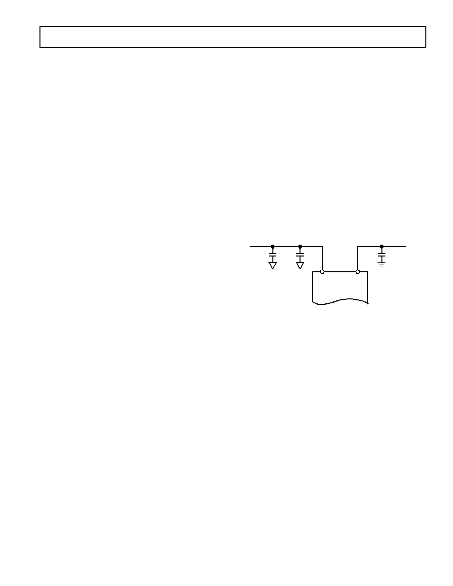
AD7710
REV. F
19
Span and Offset Limits
Whenever a system calibration mode is used, there are limits on
the amount of offset and span that can be accommodated. The
range of input span in both the unipolar and bipolar modes has
a minimum value of 0.8
×
V
REF
/GAIN and a maximum value of
2.1
×
V
REF
/GAIN.
The amount of offset which can be accommodated depends on
whether the unipolar or bipolar mode is being used. This offset
range is limited by the requirement that the positive full-scale
calibration limit is
1.05
×
V
REF
/GAIN. Therefore, the offset
range plus the span range cannot exceed 1.05
×
V
REF
/GAIN. If
the span is at its minimum (0.8
×
V
REF
/GAIN) the maximum
the offset can be is (0.25
×
V
REF
/GAIN).
In the bipolar mode, the system offset calibration range is again
restricted by the span range. The span range of the converter in
bipolar mode is equidistant around the voltage used for the
zero-scale point thus the offset range plus half the span range
cannot exceed (1.05
×
V
REF
/GAIN). If the span is set to
2 ×
V
REF
/
GAIN, the offset span cannot move more than
±
(0.05
×
V
REF
/
GAIN) before the endpoints of the transfer function exceed the
input overrange limits
±
(1.05
×
V
REF
/GAIN). If the span range
is set to the minimum
±
(0.4
×
V
REF
/GAIN) the maximum
al-
lowable offset range is
±
(0.65
×
V
REF
/GAIN).
POWER-UP AND CALIBRATION
On power-up, the AD7710 performs an internal reset which sets
the contents of the control register to a known state. However,
to ensure correct calibration for the device a calibration routine
should be performed after power-up.
The power dissipation and temperature drift of the AD7710 are
low and no warm up time is required before the initial calibra-
tion is performed. However, if an external reference is being
used, this reference must have stabilized before calibration is
initiated.
Drift Considerations
The AD7710 uses chopper stabilization techniques to minimize
input offset drift. Charge injection in the analog switches and dc
leakage currents at the sampling node are the primary sources of
offset voltage drift in the converter. The dc input leakage cur-
rent is essentially independent of the selected gain. Gain drift
within the converter depends primarily upon the temperature
tracking of the internal capacitors. It is not affected by leakage
currents.
Measurement errors due to offset drift or gain drift can be elimi-
nated at any time by recalibrating the converter or by operating
the part in the background calibration mode. Using the system
calibration mode can also minimize offset and gain errors in the
signal conditioning circuitry. Integral and differential linearity
errors are not significantly affected by temperature changes.
POWER SUPPLIES AND GROUNDING
Since the analog inputs and reference input are differential,
most of the voltages in the analog modulator are common-mode
voltages. V
BIAS
provides the return path for most of the analog
currents flowing in the analog modulator. As a result, the V
BIAS
input should be driven from a low impedance to minimize errors
due to charging/discharging impedances on this line. When the
internal reference is used as the reference source for the part,
AGND is the ground return for this reference voltage.
The analog and digital supplies to the AD7710 are independent
and separately pinned out to minimize coupling between the
analog and digital sections of the device. The digital filter will
provide rejection of broadband noise on the power supplies,
except at integer multiples of the modulator sampling frequency.
The digital supply (DV
DD
) must not exceed the analog positive
supply (AV
DD
) by more than 0.3 V in normal operation. If sepa-
rate analog and digital supplies are used, the recommended
decoupling scheme is shown in Figure 9. In systems where
AV
DD
= +5 V and DV
DD
= +5 V, it is recommended that AV
DD
and DV
DD
are driven from the same +5 V supply, although each
supply should be decoupled separately as shown in Figure 9. It
is preferable that the common supply is the system's analog +5 V
supply.
It is also important that power is applied to the AD7710 before
signals at REF IN, AIN or the logic input pins in order to avoid
excessive current. If separate supplies are used for the AD7710
and the system digital circuitry, then the AD7710 should be
powered up first. If it is not possible to guarantee this, then
current limiting resistors should be placed in series with the
logic inputs.
AD7710
0.1 F
0.1 F
10 F
ANALOG
SUPPLY
DIGITAL +5V
SUPPLY
AV
DD
DV
DD
Figure 9. Recommended Decoupling Scheme
DIGITAL INTERFACE
The AD7710's serial communications port provides a flexible
arrangement to allow easy interfacing to industry-standard
microprocessors, microcontrollers and digital signal processors.
A serial read to the AD7710 can access data from the output
register, the control register or from the calibration registers. A
serial write to the AD7710 can write data to the control register
or the calibration registers.
Two different modes of operation are available, optimized for
different types of interface where the AD7710 can act either as
master in the system (it provides the serial clock) or as slave (an
external serial clock can be provided to the AD7710). These
two modes, labelled self-clocking mode and external clocking
mode, are discussed in detail in the following sections.
Self-Clocking Mode
The AD7710 is configured for its self-clocking mode by tying
the MODE pin high. In this mode, the AD7710 provides the
serial clock signal used for the transfer of data to and from the
AD7710. This self-clocking mode can be used with processors
that allow an external device to clock their serial port including
most digital signal processors and microcontrollers such as the
68HC11 and 68HC05. It also allows easy interfacing to serial-
parallel conversion circuits in systems with parallel data commu-
nication, allowing interfacing to 74XX299 Universal Shift
registers without any additional decoding. In the case of shift
registers, the serial clock line should have a pull-down resistor
instead of the pull-up resistor shown in Figure 10 and Figure 11.
REV. F
20
AD7710
Read Operation
Data can be read from either the output register, the control
register or the calibration registers. A0 determines whether the
data read accesses data from the control register or from the
output/calibration registers. This A0 signal must remain valid
for the duration of the serial read operation. With A0 high, data
is accessed from either the output register or from the calibra-
tion registers. With A0 low, data is accessed from the control
register.
The function of the
DRDY line is dependent only on the output
update rate of the device and the reading of the output data
register.
DRDY goes low when a new data word is available in
the output data register. It is reset high when the last bit of data
(either 16th bit or 24th bit) is read from the output register. If
data is not read from the output register, the
DRDY line will
remain low. The output register will continue to be updated at
the output update rate but
DRDY will not indicate this. A read
from the device in this circumstance will access the most recent
word in the output register. If a new data word becomes avail-
able to the output register while data is being read from the
output register,
DRDY will not indicate this and the new data
word will be lost to the user.
DRDY is not affected by reading
from the control register or the calibration registers.
Data can only be accessed from the output data register when
DRDY is low. If RFS goes low with DRDY high, no data trans-
fer will take place.
DRDY does not have any effect on reading
data from the control register or from the calibration registers.
Figure 10 shows a timing diagram for reading from the AD7710
in the self-clocking mode. This read operation shows a read
from the AD7710's output data register. A read from the con-
trol register or calibration registers is similar but in these cases
the
DRDY line is not related to the read function. Depending
on the output update rate, it can go low at any stage in the con-
trol/calibration register read cycle without affecting the read and
its status should be ignored. A read operation from either the
control or calibration registers must always read 24 bits of data
from the respective register.
Figure 10 shows a read operation from the AD7710. For the
timing diagram shown, it is assumed that there is a pull-up
resistor on the SCLK output. With
DRDY low, the RFS input
is brought low.
RFS going low enables the serial clock of the
AD7710 and also places the MSB of the word on the serial data
line. All subsequent data bits are clocked out on a high to low
transition of the serial clock and are valid prior to the following
rising edge of this clock. The final active falling edge of SCLK
clocks out the LSB and this LSB is valid prior to the final active
rising edge of SCLK. Coincident with the next falling edge of
SCLK,
DRDY is reset high. DRDY going high turns off the
SCLK and the SDATA outputs. This means that the data hold
time for the LSB is slightly shorter than for all other bits.
SDATA (O)
SCLK (O)
THREE-STATE
RFS (I)
A0 (I)
t
4
t
5
t
7
t
8
t
10
9
t
DRDY (O)
t
6
t
3
MSB
LSB
t
2
Figure 10. Self-Clocking Mode, Output Data Read Operation
AD7710
REV. F
21
Read Operation
As with the self-clocking mode, data can be read from either the
output register, the control register or the calibration registers.
A0 determines whether the data read accesses data from the
control register or from the output/calibration registers. This A0
signal must remain valid for the duration of the serial read
operation. With A0 high, data is accessed from either the output
register or from the calibration registers. With A0 low, data is
accessed from the control register.
The function of the
DRDY line is dependent only on the output
update rate of the device and the reading of the output data
register.
DRDY goes low when a new data word is available in
the output data register. It is reset high when the last bit of data
(either 16th bit or 24th bit) is read from the output register. If
data is not read from the output register, the
DRDY line will
remain low. The output register will continue to be updated at
the output update rate but
DRDY will not indicate this. A read
from the device in this circumstance will access the most recent
word in the output register. If a new data word becomes avail-
able to the output register while data is being read from the
output register,
DRDY will not indicate this and the new data
word will be lost to the user.
DRDY is not affected by reading
from the control register or the calibration register.
Data can only be accessed from the output data register when
DRDY is low. If RFS goes low while DRDY is high, no data
transfer will take place.
DRDY does not have any effect on read-
ing data from the control register or from the calibration
registers.
Write Operation
Data can be written to either the control register or calibration
registers. In either case, the write operation is not affected by
the
DRDY line and the write operation does not have any effect
on the status of
DRDY. A write operation to the control register
or the calibration register must always write 24 bits to the re-
spective register.
Figure 11 shows a write operation to the AD7710. A0 deter-
mines whether a write operation transfers data to the control
register or to the calibration registers. This A0 signal must re-
main valid for the duration of the serial write operation. The
falling edge of
TFS enables the internally generated SCLK
output. The serial data to be loaded to the AD7710 must be
valid on the rising edge of this SCLK signal. Data is clocked
into the AD7710 on the rising edge of the SCLK signal with the
MSB transferred first. On the last active high time of SCLK, the
LSB is loaded to the AD7710. Subsequent to the next falling
edge of SCLK, the SCLK output is turned off. (The timing
diagram of Figure 11 assumes a pull-up resistor on the SCLK
line.)
External Clocking Mode
The AD7710 is configured for its external clocking mode by
tying the MODE pin low. In this mode, SCLK of the AD7710
is configured as an input and an external serial clock must be
provided to this SCLK pin. This external clocking mode is
designed for direct interface to systems which provide a serial
clock output that is synchronized to the serial data output,
including microcontrollers such as the 80C51, 87C51, 68HC11
and 68HC05 and most digital signal processors.
SDATA (I)
SCLK (O)
TFS (I)
A0 (I)
t
14
t
15
t
18
t
19
t
10
9
t
t
16
MSB
LSB
t
17
Figure 11. Self-Clocking Mode, Control/Calibration Register Write Operation
REV. F
22
AD7710
Figures 12a and 12b show timing diagrams for reading from the
AD7710 in the external clocking mode. Figure 12a shows a
situation where all the data is read from the AD7710 in one read
operation. Figure 12b shows a situation where the data is read
from the AD7710 over a number of read operations. Both read
operations show a read from the AD7710's output data register.
A read from the control register or calibration registers is similar
but in these cases the
DRDY line is not related to the read func-
tion. Depending on the output update rate, it can go low at any
stage in the control/calibration register read cycle without affect-
ing the read and its status should be ignored. A read operation
from either the control or calibration registers must always read
24 bits of data from the respective register.
Figure 12a shows a read operation from the AD7710 where
RFS remains low for the duration of the data word transmission.
With
DRDY low, the RFS input is brought low. The input
SCLK signal should be low between read and write operations.
RFS going low places the MSB of the word to be read on the
serial data line. All subsequent data bits are clocked out on a
high to low transition of the serial clock and are valid prior to
the following rising edge of this clock. The penultimate falling
edge of SCLK clocks out the LSB and the final falling edge
resets the
DRDY line high. This rising edge of DRDY turns off
the serial data output.
Figure 12b shows a timing diagram for a read operation where
RFS returns high during the transmission of the word and
returns low again to access the rest of the data word. Timing
parameters and functions are very similar to that outlined for
Figure 12a but Figure 12b has a number of additional times to
show timing relationships when
RFS returns high in the middle
of transferring a word.
RFS should return high during a low time of SCLK. On the
rising edge of
RFS, the SDATA output is turned off. DRDY
remains low and will remain low until all bits of the data word
are read from the AD7710, regardless of the number of times
RFS changes state during the read operation. Depending on the
time between the falling edge of SCLK and the rising edge of
RFS, the next bit (BIT N+1) may appear on the databus before
RFS goes high. When RFS returns low again, it activates the
SDATA output. When the entire word is transmitted, the
DRDY line will go high turning off the SDATA output as per
Figure 12a.
RFS (I)
SCLK (I)
SDATA (O)
t
24
t
28
LSB
t
26
MSB
t
29
THREE-STATE
t
20
A0 (I)
t
22
t
23
t
21
t
27
t
25
DRDY (O)
Figure 12a. External-Clocking Mode, Output Data Read Operation
THREE-STATE
t
27
t
26
MSB
t
30
t
31
BIT N
t
24
t
25
BIT N+1
SDATA (O)
SCLK (I)
RFS (I)
t
20
A0 (I)
DRDY (O)
t
22
t
24
t
25
Figure 12b. External-Clocking Mode, Output Data Read Operation (
RFS Returns High During Read Operation)
AD7710
REV. F
23
Write Operation
Data can be written to either the control register or calibration
registers. In either case, the write operation is not affected by
the
DRDY line and the write operation does not have any effect
on the status of
DRDY. A write operation to the control register
or the calibration register must always write 24 bits to the
respective register.
Figure 13a shows a write operation to the AD7710 with
TFS
remaining low for the duration of the write operation. A0 deter-
mines whether a write operation transfers data to the control
register or to the calibration registers. This A0 signal must
remain valid for the duration of the serial write operation. As
before, the serial clock line should be low between read and
write operations. The serial data to be loaded to the AD7710
must be valid on the high level of the externally applied SCLK
signal. Data is clocked into the AD7710 on the high level of this
SCLK signal with the MSB transferred first. On the last active
high time of SCLK, the LSB is loaded to the AD7710.
Figure 13b shows a timing diagram for a write operation to the
AD7710 with
TFS returning high during the write operation
and returning low again to write the rest of the data word. Tim-
ing parameters and functions are very similar to that outlined for
Figure 13a, but Figure 13b has a number of additional times to
show timing relationships when
TFS returns high in the middle
of transferring a word.
Data to be loaded to the AD7710 must be valid prior to the
rising edge of the SCLK signal.
TFS should return high during
the low time of SCLK. After
TFS returns low again, the next bit
of the data word to be loaded to the AD7710 is clocked in on
next high level of the SCLK input. On the last active high time
of the SCLK input, the LSB is loaded to the AD7710.
t
35
t
33
SCLK (I)
SDATA (I)
A0 (I)
t
32
MSB
LSB
t
26
t
27
t
34
TFS
(I)
t
36
Figure 13a. External-Clocking Mode, Control/Calibration Register Write Operation
t
35
SCLK (I)
SDATA (I)
TFS
(I)
A0 (I)
MSB
BIT N
BIT N+1
t
32
t
26
t
30
t
27
t
36
t
35
t
36
Figure 13b. External-Clocking Mode, Control/Calibration Register Write Operation
(
TFS Returns High During Write Operation)
REV. F
24
AD7710
SIMPLIFYING THE EXTERNAL CLOCKING MODE
INTERFACE
In many applications, the user may not require the facility of
writing to the on-chip calibration registers. In this case, the
serial interface to the AD7710 in external clocking mode can be
simplified by connecting the
TFS line to the A0 input of the
AD7710 (see Figure 14). This means that any write to the de-
vice will load data to the control register (since A0 is low while
TFS is low) and any read to the device will access data from the
output data register or from the calibration registers (since A0 is
high while
RFS is low). It should be noted that in this arrange-
ment the user does not have the capability of reading from the
control register.
AD7710
SDATA
SCLK
TFS
A0
FOUR
INTERFACE
LINES
RFS
Figure 14. Simplified Interface with
TFS Connected to A0
Another method of simplifying the interface is to generate the
TFS signal from an inverted RFS signal. However, generating
the signals the opposite way around (
RFS from an inverted
TFS) will cause writing errors.
MICROCOMPUTER/MICROPROCESSOR INTERFACING
The AD7710's flexible serial interface allows for easy interface
to most microcomputers and microprocessors. Figure 15 shows
a flowchart diagram for a typical programming sequence for
reading data from the AD7710 to a microcomputer while Figure
16 shows a flowchart diagram for writing data to the AD7710.
Figures 17, 18 and 19 show some typical interface circuits.
The flowchart of Figure 15 is for continuous read operations
from the AD7710 output register. In the example shown, the
DRDY line is continuously polled. Depending on the micro-
processor configuration, the
DRDY line may come to an inter-
rupt input in which case the
DRDY will automatically generate
an interrupt without being polled. The reading of the serial
buffer could be anything from one read operation up to three
read operations (where 24 bits of data are read into an 8-bit
serial register). A read operation to the control/calibration regis-
ters is similar but in this case the status of
DRDY can be
ignored. The A0 line is brought low when the
RFS line is
brought low when reading from the control register.
The flowchart also shows the bits being reversed after they have
been read in from the serial port. This depends on whether the
microprocessor expects the MSB of the word first or the LSB of
the word first. The AD7710 outputs the MSB first.
The flowchart for Figure 16 is for a single 24-bit write operation
to the AD7710 control or calibration registers. This shows data
being transferred from data memory to the accumulator before
being written to the serial buffer. Some microprocessor systems
will allow data to be written directly to the serial buffer from
data memory. The writing of data to the serial buffer from the
accumulator will generally consist of either two or three write
operations, depending on the size of the serial buffer.
NO
YES
BRING
RFS LOW
x3
REVERSE
ORDER OF BITS
BRING
RFS HIGH
POLL DRDY
CONFIGURE &
INITIALIZE C/ P
SERIAL PORT
DRDY
LOW?
BRING
RFS, TFS HIGH
START
READ
SERIAL BUFFER
Figure 15. Flowchart for Continuous Read Operations to
the AD7710
The flowchart also shows the option of the bits being reversed
before being written to the serial buffer. This depends on
whether the first bit transmitted by the microprocessor is the
MSB or the LSB. The AD7710 expects the MSB as the first bit
in the data stream. In cases where the data is being read or
being written in bytes and the data has to be reversed, the bits
will have to be reversed for every byte.
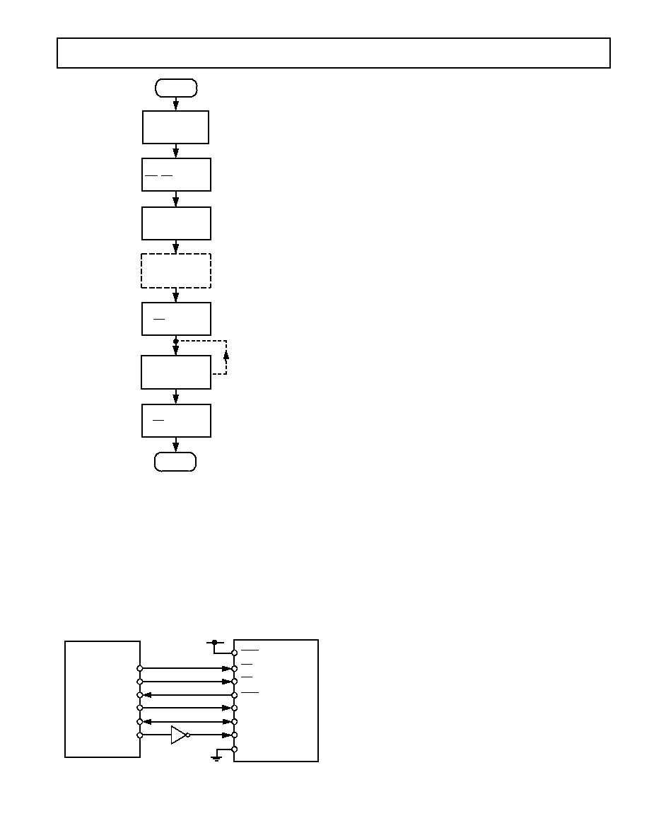
AD7710
REV. F
25
REVERSE
ORDER OF
BITS
x3
START
WRITE DATA FROM
ACCUMULATOR TO
SERIAL BUFFER
BRING
TFS & A0 LOW
LOAD DATA FROM
ADDRESS TO
ACCUMULATOR
CONFIGURE &
INITIALIZE C/ P
SERIAL PORT
BRING
RFS, TFS & A0 HIGH
BRING
TFS & A0 HIGH
END
Figure 16. Flowchart for Single Write Operation to the
AD7710
AD7710 to 8XC51 Interface
Figure 17 shows an interface between the AD7710 and the
8XC51 microcontroller. The AD7710 is configured for its exter-
nal clocking mode while the 8XC51 is configured in its Mode 0
serial interface mode. The
DRDY line from the AD7710 is
connected to the Port P1.2 input of the 8XC51 so the
DRDY
line is polled by the 8XC51. The
DRDY line can be connected
to the
INT1 input of the 8XC51 if an interrupt driven system is
preferred.
P1.0
P3.0
P3.1
P1.1
P1.2
P1.3
8XC51
AD7710
SDATA
A0
RFS
TFS
MODE
DRDY
SYNC
SCLK
DV
DD
Figure 17. AD7710 to 8XC51 Interface
Table VII shows some typical 8XC51 code used for a single 24-
bit read from the output register of the AD7710. Table VIII
shows some typical code for a single write operation to the con-
trol register of the AD7710. The 8XC51 outputs the LSB first
in a write operation while the AD7710 expects the MSB first so
the data to be transmitted has to be rearranged before being
written to the output serial register. Similarly, the AD7710
outputs the MSB first during a read operation while the 8XC51
expects the LSB first. Therefore, the data which is read into the
serial buffer needs to be rearranged before the correct data word
from the AD7710 is available in the accumulator.
Table VII. 8XC51 Code for Reading from the AD7710
MOV SCON,#00010001B;
Configure 8051 for MODE 0
Operation
MOV IE,#00010000B;
Disable All Interrupts
SETB 90H;
Set P1.0, Used as
RFS
SETB 91H;
Set P1.1, Used as
TFS
SETB 93H;
Set P1.3, Used as A0
MOV R1,#003H;
Sets Number of Bytes to Be Read in
A Read Operation
MOV R0,#030H;
Start Address for Where Bytes Will
Be Loaded
MOV R6,#004H;
Use P1.2 as
DRDY
WAIT:
NOP;
MOV A,P1;
Read Port 1
ANL A,R6;
Mask Out All Bits Except
DRDY
JZ READ;
If Zero Read
SJMP WAIT;
Otherwise Keep Polling
READ:
CLR 90H;
Bring
RFS Low
CLR 98H;
Clear Receive Flag
POLL:
JB 98H, READ1
Tests Receive Interrupt Flag
SJMP POLL
READ 1:
MOV A,SBUF;
Read Buffer
RLC A;
Rearrange Data
MOV B.0,C;
Reverse Order of Bits
RLC A; MOV B.1,C; RLC A; MOV B.2,C;
RLC A; MOV B.3,C; RLC A; MOV B.4,C;
RLC A; MOV B.5,C; RLC A; MOV B.6,C;
RLC A; MOV B.7,C;
MOV A,B;
MOV @R0,A;
Write Data to Memory
INC R0;
Increment Memory Location
DEC R1
Decrement Byte Counter
MOV A,R1
JZ END
Jump if Zero
JMP WAIT
Fetch Next Byte
END:
SETB 90H
Bring
RFS High
FIN:
SJMP FIN
REV. F
26
AD7710
Table VIII. 8XC51 Code for Writing to the AD7710
MOV SCON,#00000000B;
Configure 8051 for MODE 0
Operation & Enable Serial Reception
MOV IE,#10010000B;
Enable Transmit Interrupt
MOV IP,#00010000B;
Prioritize the Transmit Interrupt
SETB 91H;
Bring
TFS High
SETB 90H;
Bring
TFS High
MOV R1,#003H;
Sets Number of Bytes to Be Written
in a Write Operation
MOV R0,#030H;
Start Address in RAM for Bytes
MOV A,#00H;
Clear Accumulator
MOV SBUF,A;
Initialize the Serial Port
WAIT:
JMP WAIT;
Wait for Interrupt
INT ROUTINE:
NOP;
Interrupt Subroutine
MOV A,R1;
Load R1 to Accumulator
JZ FIN;
If Zero Jump to FIN
DEC R1;
Decrement R1 Byte Counter
MOV A,@R;
Move Byte into the Accumulator
INC R0;
Increment Address
RLC A;
Rearrange Data--From LSB First
to MSB First
MOV B.0,C; RLC A; MOV B.1,C; RLC A;
MOV B.2,C; RLC A; MOV B.3,C; RLC A;
MOV B.4,C; RLC A; MOV B.5,C; RLC A;
MOV B.6,C; RLC A: MOV B.7,C; MOV A,B;
CLR 93H;
Bring A0 Low
CLR 91H;
Bring
TFS Low
MOV SBUF,A;
Write to Serial Port
RETI;
Return from Subroutine
FIN:
SETB 91H;
Set
TFS High
SETB 93H;
Set A0 High
RETI;
Return from Interrupt Subroutine
AD7710 to 68HC11 Interface
Figure 18 shows an interface between the AD7710 and the
68HC11 microcontroller. The AD7710 is configured for its
external clocking mode while the SPI port is used on the
68HC11 which is in its single chip mode. The
DRDY line from
the AD7710 is connected to the Port PC0 input of the 68HC11
so the
DRDY line is polled by the 68HC11. The DRDY line
can be connected to the
IRQ input of the 68HC11 if an inter-
rupt driven system is preferred. The 68HC11 MOSI and MISO
lines should be configured for wired-or operation. Depending
on the interface configuration, it may be necessary to provide
bidirectional buffers between the 68HC11's MOSI and MISO
lines.
The 68HC11 is configured in the master mode with its CPOL
bit set to a logic zero and its CPHA bit set to a logic one. With a
10 MHz master clock on the AD7710, the interface will operate
with all four serial clock rates of the 68HC11.
AD7710
SDATA
SCLK
A0
RFS
TFS
PC0
MISO
SCK
PC1
PC2
MODE
PC3
DRDY
SYNC
68HC11
MOSI
SS
DV
DD
DV
DD
Figure 18. AD7710 to 68HC11 Interface
AD7710 to ADSP-2105 Interface
An interface circuit between the AD7710 and the ADSP-2105
microprocessor is shown in Figure 19. In this interface, the
AD7710 is configured for its self-clocking mode while the
RFS
and
TFS pins of the ADSP-2105 are configured as inputs and
the ADSP-2105 serial clock line is also configured as an input.
When the ADSP-2105's serial clock is configured as an input it
needs a couple of clock pulses to initialize itself correctly before
accepting data. Therefore, the first read from the AD7710 may
not read correct data. In the interface shown, a read operation
to the AD7710 accesses either the output register or the calibra-
tion registers. Data cannot be read from the control register.
A write operation always writes to the control or calibration
registers.
DRDY is used as the frame synchronization pulse for read
operations from the output register and it is decoded with A0 to
drive the
RFS inputs of both the AD7710 and the ADSP-2105.
The latched A0 line drives the
TFS inputs of both the AD7710
and the ADSP-2105 as well as the AD7710 A0 input.
AD7710
SDATA
SCLK
A0
RFS
TFS
DR
SCLK
MODE
A0
DRDY
ADSP-2105
DT
DMWR
TFS
DV
DD
D
74HC74
Q
Q
RFS
Figure 19. AD7710 to ADSP-2105 Interface
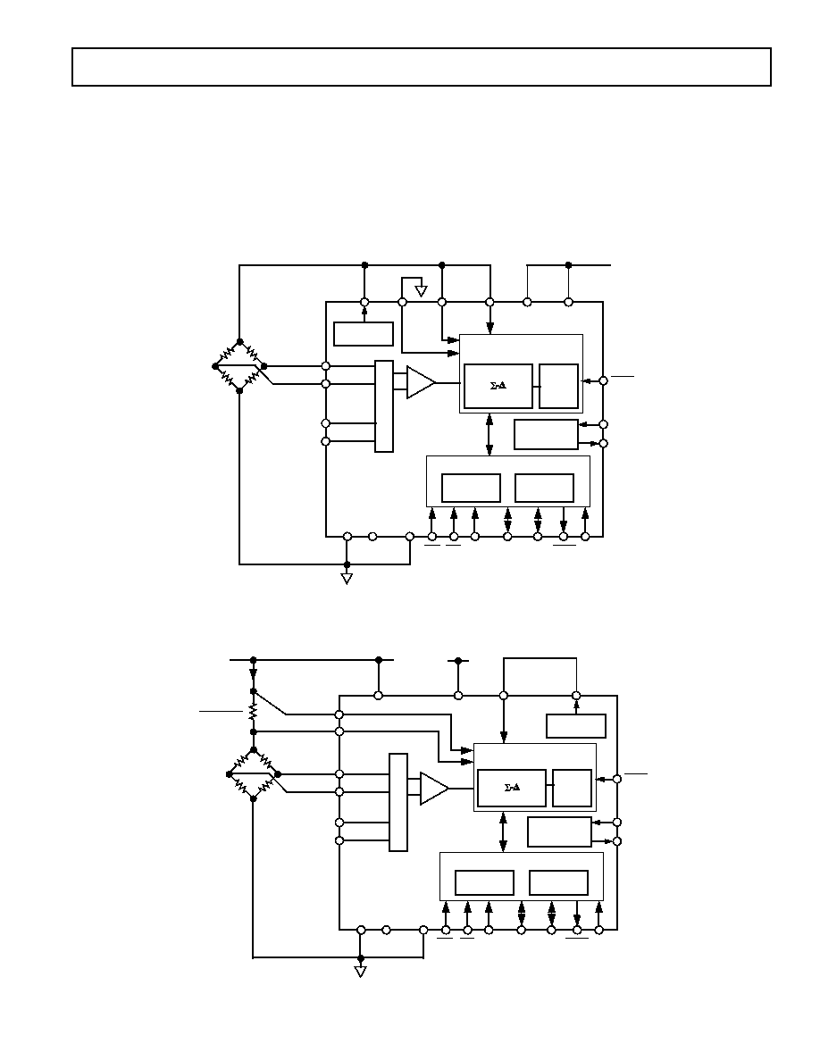
AD7710
REV. F
27
APPLICATIONS
Figure 20 shows a strain gage interfaced directly to one of the
analog input channels of the AD7710. The differential inputs to
the AD7710 are connected directly to the bridge network of the
strain gage. In the diagram shown, the on-chip reference of the
AD7710 provides the voltage for the bridge network and also
provides the reference voltage for the AD7710. An alternative
scheme, outlined in Figure 21, shows the analog positive supply
voltage powering the bridge network and the AD7710 with the
CLOCK
GENERATION
SERIAL INTERFACE
CONTROL
REGISTER
OUTPUT
REGISTER
CHARGE-BALANCING A/D
CONVERTER
DIGITAL
FILTER
AD7710
M
U
X
PGA
AGND
DGND
MODE SDATA SCLK
A0
MCLK
OUT
MCLK
I
AIN1(+)
AIN1()
REF
IN ()
REF
IN (+)
SYNC
A = 1 128
DRDY
TFS
RFS
AIN2(+)
AIN2()
V
SS
V
BIAS
AV
DD
DV
DD
2.5V
REFERENCE
REF
OUT
ANALOG
+5V SUPPLY
R
R
ACTIVE
GAGE
DUMMY
GAGE
N
AUTO-ZEROED
MODULATOR
Figure 20. Strain-Gage Application with the AD7710
CLOCK
GENERATION
SERIAL INTERFACE
CONTROL
REGISTER
OUTPUT
REGISTER
CHARGE-BALANCING A/D
CONVERTER
AUTO-ZEROED
MODULATOR
DIGITAL
FILTER
AD7710
M
U
X
PGA
AGND
DGND
MODE SDATA SCLK
A0
MCLK
OUT
MCLK
IN
AIN1(+)
AIN1()
SYNC
A = 1 128
DRDY
TFS
RFS
AIN2(+)
AIN2()
V
SS
V
BIAS
AV
DD
DV
DD
2.5V
REFERENCE
R
R
ACTIVE
GAGE
DUMMY
GAGE
DIGITAL
+5V SUPPLY
ANALOG SUPPLY
EXCITATION
CURRENT
REF IN(+)
R =
V
REF
I
EXCITATION
REF IN()
REF
OUT
Figure 21. Alternate Scheme for Generating AD7710 Reference Voltage
reference voltage for the AD7710 generated across a resistor
which is placed in series with the bridge network. In this case,
the value of the reference resistor is determined by the required
reference voltage divided by the value of the excitation current.
The on-chip PGA allows the AD7710 to handle an analog input
voltage range as low as 20 mV full scale. The differential inputs
of the part allow this analog input range to have an absolute
value anywhere between V
SS
and AV
DD
.
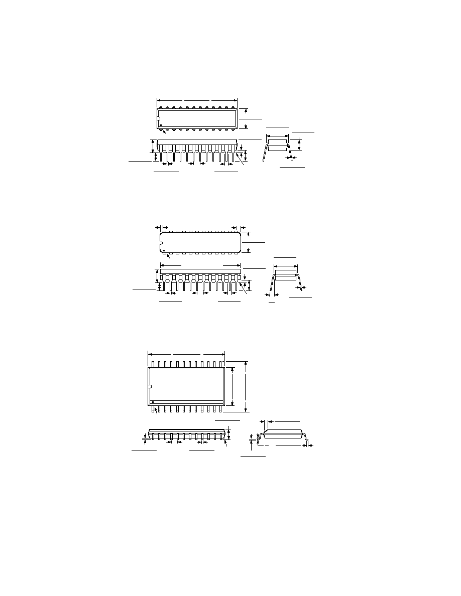
REV. F
28
AD7710
OUTLINE DIMENSIONS
Dimensions shown in inches and (mm).
Plastic DIP (N-24)
24
1
12
13
0.280 (7.11)
0.240 (6.10)
PIN 1
1.275 (32.30)
1.125 (28.60)
0.150
(3.81)
MIN
0.200 (5.05)
0.125 (3.18)
SEATING
PLANE
0.022 (0.558)
0.014 (0.356)
0.060 (1.52)
0.015 (0.38)
0.210
(5.33)
MAX
0.070 (1.77)
0.045 (1.15)
0.100 (2.54)
BSC
0.325 (8.25)
0.300 (7.62)
0.015 (0.381)
0.008 (0.204)
0.195 (4.95)
0.115 (2.93)
Cerdip (Q-24)
24
1
12
13
0.310 (7.87)
0.220 (5.59)
PIN 1
0.005 (0.13) MIN
0.098 (2.49) MAX
SEATING
PLANE
0.023 (0.58)
0.014 (0.36)
0.200 (5.08)
MAX
1.280 (32.51) MAX
0.150
(3.81)
MIN
0.200 (5.08)
0.125 (3.18)
0.100 (2.54)
BSC
0.060 (1.52)
0.015 (0.38)
0.070 (1.78)
0.030 (0.76)
15°
0°
0.320 (8.13)
0.290 (7.37)
0.015 (0.38)
0.008 (0.20)
SOIC (R-24)
24
13
12
1
0.6141 (15.60)
0.5985 (15.20)
0.4193 (10.65)
0.3937 (10.00)
0.2992 (7.60)
0.2914 (7.40)
PIN 1
SEATING
PLANE
0.0118 (0.30)
0.0040 (0.10)
0.0192 (0.49)
0.0138 (0.35)
0.1043 (2.65)
0.0926 (2.35)
0.0500
(1.27)
BSC
0.0125 (0.32)
0.0091 (0.23)
0.0500 (1.27)
0.0157 (0.40)
8°
0°
0.0291 (0.74)
0.0098 (0.25)
x 45°
C1654e010/99
PRINTED IN U.S.A.