Äîêóìåíòàöèÿ è îïèñàíèÿ www.docs.chipfind.ru
REV. D
Information furnished by Analog Devices is believed to be accurate and
reliable. However, no responsibility is assumed by Analog Devices for its
use, nor for any infringements of patents or other rights of third parties
which may result from its use. No license is granted by implication or
otherwise under any patent or patent rights of Analog Devices.
a
LC
2
MOS
20-Bit A/D Converter
AD7703
© Analog Devices, Inc., 1996
One Technology Way, P.O. Box 9106, Norwood, MA 02062-9106, U.S.A.
Tel: 617/329-4700
Fax: 617/326-8703
FEATURES
Monolithic 20-Bit ADC
0.0003% Linearity Error
20-Bit No Missed Codes
On-Chip Self-Calibration Circuitry
Programmable Low-Pass Filter
0.1 Hz to 10 Hz Corner Frequency
0 to +2.5 V or +2.5 V Analog Input Range
4 kSPS Output Data Rate
Flexible Serial Interface
Ultralow Power
APPLICATIONS
Industrial Process Control
Weigh Scales
Portable Instrumentation
Remote Data Acquisition
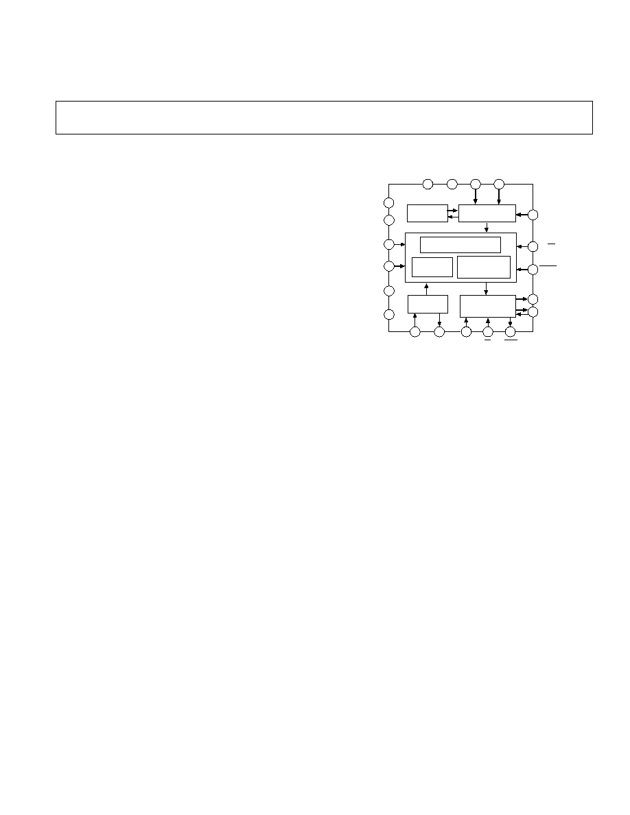
FUNCTIONAL BLOCK DIAGRAM
5
DGND
AV
DD
DV
DD
AV
SS
DV
SS
SC1
SC2
14
15
7
6
4
17
AGND
A
IN
V
REF
10
8
13
CALIBRATION
SRAM
CALIBRATION
MICROCONTROLLER
CAL
BP/UP
SLEEP
20
19
CLOCK
GENERATOR
SERIAL INTERFACE
LOGIC
SDATA
SCLK
3
2
1
16
18
CLKIN
CLKOUT
MODE
CS
DRDY
AD7703
9
ANALOG
MODULATOR
12
11
6-POLE GAUSSIAN
LOW-PASS
DIGITAL FILTER
20-BIT CHARGE BALANCE A/D
CONVERTER
PRODUCT HIGHLIGHTS
1. The AD7703 offers 20-bit resolution coupled with
outstanding 0.0003% accuracy.
2. No missing codes ensures true, usable, 20-bit dynamic range,
removing the need for programmable gain and level-setting
circuitry.
3. The effects of temperature drift are eliminated by on-chip
self-calibration, which removes zero and gain error. External
circuits can also be included in the calibration loop to remove
system offsets and gain errors.
4. A flexible synchronization allows the AD7703 to interface
directly to the serial ports of industry standard
microcontrollers and DSP processors.
5. Low operating power consumption and an ultralow power
standby mode make the AD7703 ideal for loop powered
remote sensing applications, or battery-powered portable
instruments.
GENERAL DESCRIPTION
The AD7703 is a 20-bit ADC which uses a sigma delta conver-
sion technique. The analog input is continuously sampled by an
analog modulator whose mean output duty cycle is proportional
to the input signal. The modulator output is processed by an
on-chip digital filter with a six-pole Gaussian response, which
updates the output data register with 20-bit binary words at
word rates up to 4 kHz. The sampling rate, filter corner fre-
quency and output word rate are set by a master clock input
that may be supplied externally, or by an on-chip gate oscillator.
The inherent linearity of the ADC is excellent, and endpoint
accuracy is ensured by self-calibration of zero and full scale
which may be initiated at any time. The self-calibration scheme
can also be extended to null system offset and gain errors in the
input channel.
The output data is accessed through a serial port, which has two
synchronous modes suitable for interfacing to shift registers or
the serial ports of industry standard microcontrollers.
CMOS construction ensures low power dissipation, and a power
down mode reduces the idle power consumption to only 10 W.

REV. D
2
AD7703SPECIFICATIONS
Parameter
A/S Versions
2
B Version
2
C Version
2
Units
Test Conditions/Comments
STATIC PERFORMANCE
Resolution
20
20
20
Bits
Integral Nonlinearity, T
MIN
to T
MAX
±
0.0015
±
0.0007
±
0.0003
% FSR typ
+25
°
C
±
0.003
±
0.0015
±
0.0008
% FSR max
T
MIN
to T
MAX
±
0.003
±
0.0015
±
0.0012
% FSR max
Differential Nonlinearity, T
MIN
to T
MAX
±
0.5
±
0.5
±
0.5
LSB typ
Guaranteed No Missing Codes
Positive Full-Scale Error
3
±
4
±
4
±
4
LSB typ
±
16
±
16
±
16
LSB max
Full-Scale Drift
4
±
19/
±
37
±
19
±
19
LSB typ
Unipolar Offset Error
3
±
4
±
4
±
4
LSB typ
±
16
±
16
±
16
LSB max
Unipolar Offset Drift
4
±
26
±
26
±
26
LSB typ
Temp Range: 0
°
C to +70
°
C
±
67 +48/400
±
67
±
67
LSB typ
Specified Temp Range
Bipolar Zero Error
3
±
4
±
4
±
4
LSB typ
±
16
±
16
±
16
LSB max
Bipolar Zero Drift
4
±
13
±
13
±
13
LSB typ
Temp Range: 0
°
C to +70
°
C
±
34 +24/200
±
34
±
34
LSB typ
Specified Temp Range
Bipolar Negative Full-Scale Errors
3
±
8
±
8
±
8
LSB typ
±
32
±
32
±
32
LSB max
Bipolar Negative Full-Scale Drift
4
±
10/
±
20
±
10
±
10
LSB typ
Noise (Referred to Output)
1.6
1.6
1.6
LSB rms typ
DYNAMIC PERFORMANCE
Sampling Frequency, f
S
f
CLKIN
/256
f
CLKIN
/256
f
CLKIN
/256
Hz
Output Update Rate, f
OUT
f
CLKIN
/1024
f
CLKIN
/1024
f
CLKIN
/1024
Hz
Filter Corner Frequency, f
3 dB
f
CLKIN
/409,600
f
CLKIN
/409,600
f
CLKIN
/409,600
Hz
Settling Time to
±
0.0007% FS
507904/f
CLKIN
507904/f
CLKIN
507904/f
CLKIN
sec
For Full-Scale Input Step
SYSTEM CALIBRATION
Positive Full-Scale Calibration Range
V
REF
+ 0.1
V
REF
+ 0.1
V
REF
+ 0.1
V max
System Calibration Applies to
Positive Full-Scale Overrange
V
REF
+ 0.1
V
REF
+ 0.1
V
REF
+ 0.1
V max
Unipolar and Bipolar Ranges.
Negative Full-Scale Overrange
(V
REF
+ 0.1)
(V
REF
+ 0.1)
(V
REF
+ 0.1)
V max
After Calibration, if A
IN
> V
REF
,
Maximum Offset Calibration Ranges
5, 6
the Device Will Output All 1s.
Unipolar Input Range
(V
REF
+ 0.1)
(V
REF
+ 0.1)
(V
REF
+ 0.1)
V max
If A
IN
< 0 (Unipolar) or V
REF
Bipolar Input Range
0.4 V
REF
to +0.4 V
REF
0.4 V
REF
to +0.4 V
REF
0.4 V
REF
to +0.4 V
REF
V max
(Bipolar), the Device Will
Input Span
7
0.8 V
REF
0.8 V
REF
0.8 V
REF
V min
Output all 0s
2 V
REF
+ 0.2
2 V
REF
+ 0.2
2 V
REF
+ 0.2
V max
ANALOG INPUT
Unipolar Input Range
0 to +2.5
0 to +2.5
0 to +2.5
Volts
Bipolar Input Range
±
2.5
±
2.5
±
2.5
Volts
Input Capacitance
20
20
20
pF typ
Input Bias Current
1
1
1
1
nA typ
LOGIC INPUTS
All Inputs except CLKIN
V
INL
, Input Low Voltage
0.8
0.8
0.8
V max
V
INH
, Input High Voltage
2.0
2.0
2.0
V min
CLKIN
V
INL
, Input Low Voltage
0.8
0.8
0.8
V max
V
INH
, Input High Voltage
3.5
3.5
3.5
V min
I
IN
, Input Current
10
10
10
µ
A max
LOGIC OUTPUTS
V
OL
, Output Low Voltage
0.4
0.4
0.4
V max
I
SINK
= 1.6 mA
V
OH
, Output High Voltage
DV
DD
1
DV
DD
1
DV
DD
1
V min
I
SOURCE
= 100
µ
A
Floating State Leakage Current
±
10
±
10
±
10
µ
A max
Floating State Output Capacitance
9
9
9
pF typ
POWER REQUIREMENTS
Power Supply Voltages
Analog Positive Supply (AV
DD
)
4.5/5.5
4.5/5.5
4.5/5.5
V min/V max
For Specified Performance
Digital Positive Supply (DV
DD
)
4.5/AV
DD
4.5/AV
DD
4.5/AV
DD
V min/V max
Analog Negative Supply (AV
SS
)
4.5/5.5
4.5/5.5
4.5/5.5
V min/V max
Digital Negative Supply (DV
SS
)
4.5/5.5
4.5/5.5
4.5/5.5
V min/V max
Calibration Memory Retention
Power Supply Voltage
2.0
2.0
2.0
V min
(T
A
= +25 C; AV
DD
= DV
DD
= +5 V; AV
SS
= DV
SS
= 5 V; V
REF
= +2.5 V; f
CLKIN
= 4.096 MHz;
BP/UP = +5 V; MODE = +5 V; A
IN
Source Resistance = 1 k
1
with 1 nF to AGND at A
IN
unless otherwise noted.)
Parameter
A/S Versions
2
B Version
2
C Version
2
Units
Test Conditions/Comments
STATIC PERFORMANCE
DC Power Supply Currents
8
Analog Positive Supply (AI
DD
)
3.2
3.2
3.2
mA max
Typically 2 mA
Digital Positive Supply (DI
DD
)
1.5
1.5
1.5
mA max
Typically 1 mA
Analog Negative Supply (AI
SS
)
3.2
3.2
3.2
mA max
Typically 2 mA
Digital Negative Supply (DI
SS
)
0.1
0.1
0.1
mA max
Typically 0.03 mA
Power Supply Rejection
9
Positive Supplies
70
70
70
dB typ
Negative Supplies
75
75
75
dB typ
Power Dissipation
Normal Operation
40
40
40
mW rnax
SLEEP
= Logic 1,
Typically 25 mW
Standby Operations
10
SLEEP
= Logic 0,
A, B, C
20
20
20
µ
W max
Typically 10
µ
W
S
40
40
40
µ
W max
NOTES
1
The A
IN
pin presents a very high impedance dynamic load which varies with clock frequency. A ceramic 1 nF capacitor from the A
IN
to AGND is necessary. Source
resistance should be 750
or less.
2
Temperature Ranges are as follows: A, B, C Versions: 40
°
C to +85
°
C; S Version: 55
°
C to +125
°
C.
3
Applies after calibration at the temperature of interest. Full-Scale Error applies for both unipolar and bipolar input ranges.
4
Total drift over the specified temperature range after calibration at power-up at +25
°
C. This is guaranteed by design and/or characterization. Recalibration at any
temperature will remove these errors.
5
In unipolar mode the offset can have a negative value (V
REF
) such that the unipolar mode can mimic bipolar mode operation.
6
The specifications for input overrange and for input span apply additional constraints on the offset calibration range.
7
For unipolar mode, input span is the difference between full scale and zero scale. For bipolar mode, input span is the difference between positive and negative
full-scale points. When using less than the maximum input span, the span range may be placed anywhere within the range of
±
(V
REF
+ 0.1).
8
All digital outputs unloaded. All digital inputs at 5 V CMOS levels.
9
Applies in 0.1 Hz to 10 Hz bandwidth. PSRR at 60 Hz will exceed 120 dB due to the digital filter.
10
CLKIN is stopped. All digital inputs are grounded.
Specifications subject to change without notice.
ABSOLUTE MAXIMUM RATINGS*
(T
A
= +25
°
C unless otherwise noted)
DV
DD
to AGND . . . . . . . . . . . . . . . . . . . . . . . 0.3 V to +6 V
DV
DD
to AV
DD
. . . . . . . . . . . . . . . . . . . . . . . 0.3 V to +0.3 V
DV
SS
to AGND . . . . . . . . . . . . . . . . . . . . . . . . +0.3 V to 6 V
AV
DD
to AGND . . . . . . . . . . . . . . . . . . . . . . . . 0.3 V to +6 V
AV
SS
to AGND . . . . . . . . . . . . . . . . . . . . . . . . +0.3 V to 6 V
AGND to DGND . . . . . . . . . . . . . . . . . . . . . 0.3 V to +0.3 V
Digital Input Voltage to DGND . . . . 0.3 V to DV
DD
+ 0.3 V
Analog Input Voltage to AGND . . . . . . . . . . . AV
SS
0.3 V to
. . . . . . . . . . . . . . . . . . . . . . . . . . . . . . . . . . . . . . AV
DD
+ 0.3 V
Input Current to Any Pin Except Supplies
1
. . . . . . . .
±
10 mA
Operating Temperature Range
Industrial (A, B, C Versions) . . . . . . . . . . . 40
°
C to +85
°
C
Extended (S Version) . . . . . . . . . . . . . . . . 55
°
C to +125
°
C
Storage Temperature Range . . . . . . . . . . . . 65
°
C to +150
°
C
Lead Temperature (Soldering, 10 secs) . . . . . . . . . . . +300
°
C
Power Dissipation (DIP Package) to +75
°
C . . . . . . . 450 mW
Derates above +75
°
C by . . . . . . . . . . . . . . . . . . . . 10 mW/
°
C
Power Dissipation (SOIC Package) to +75
°
C . . . . . . 250 mW
Derates above +75
°
C by . . . . . . . . . . . . . . . . . . . . 15 mW/
°
C
NOTES
*Stresses above those listed under "Absolute Maximum Ratings" may cause
permanent damage to the device. This is a stress rating only and functional
operation of the device at these or any other conditions above those listed in the
operational sections of this specification is not implied. Exposure to absolute
maximum rating conditions for extended periods may affect device reliability.
1
Transient currents of up to 100 mA will not cause SCR latch-up.
ORDERING GUIDE
Linearity
Temperature
Error
Package
Model
Range
(% FSR)
Options*
AD7703AN
40
°
C to +85
°
C
0.003
N-20
AD7703BN
40
°
C to +85
°
C
0.0015
N-20
AD7703CN
40
°
C to +85
°
C
0.0012
N-20
AD7703AR
40
°
C to +85
°
C
0.003
R-20
AD7703BR
40
°
C to +85
°
C
0.0015
R-20
AD7703CR
40
°
C to +85
°
C
0.0012
R-20
AD7703AQ
40
°
C to +85
°
C
0.003
Q-20
AD7703BQ
40
°
C to +85
°
C
0.0015
Q-20
AD7703CQ
40
°
C to +85
°
C
0.0012
Q-20
AD7703SQ
55
°
C to +125
°
C
0.003
Q-20
*N = Plastic DIP; R = SOIC; Q = Cerdip.
WARNING!
ESD SENSITIVE DEVICE
CAUTION
ESD (electrostatic discharge) sensitive device. Electrostatic charges as high as 4000 V readily
accumulate on the human body and test equipment and can discharge without detection.
Although this device features proprietary ESD protection circuitry, permanent damage may
occur on devices subjected to high energy electrostatic discharges. Therefore, proper ESD
precautions are recommended to avoid performance degradation or loss of functionality.
3
AD7703
REV. D
AD7703
4
REV. D
(AV
DD
= DV
DD
= +5 V 10%; AV
SS
= DV
SS
= 5 V 10%; AGND = DGND = 0 V; f
CLKIN
=
4.096 MHz; Input Levels: Logic 0 = 0 V, Logic 1 = DV
DD
; unless otherwise noted.)
TIMING CHARACTERISTICS
1, 2
Limit at T
MIN
, T
MAX
Limit at T
MIN
, T
MAX
Parameter
(A, B, C Versions)
(S Version)
Units
Conditions/Comment
6
f
CLKIN
3, 4
200
200
kHz min
Master Clock Frequency: Internal Gate Oscillator
5
5
MHz max Typically 4096 kHz
200
200
kHz min
Master Clock Frequency: Externally Supplied
5
5
MHz max
t
r
5
50
50
ns max
Digital Output Rise Time. Typically 20 ns
t
f
5
50
50
ns max
Digital Output Fall Time. Typically 20 ns
t
1
0
0
ns min
SC1, SC2 to CAL High Setup Time
t
2
50
50
ns min
SC1, SC2 Hold Time After CAL Goes High
t
3
6
1000
1000
ns min
SLEEP
High to CLKIN High Setup Time
SSC MODE
t
4
7
3/f
CLKIN
3/f
CLKIN
ns max
Data Access Time (CS Low to Data Valid)
t
5
100
100
ns max
SCLK Falling Edge to Data Valid Delay (25 ns typ)
t
6
250
250
ns min
MSB Data Setup Time. Typically 380 ns
t
7
300
300
ns max
SCLK High Pulse Width. Typically 240 ns
t
8
790
790
ns max
SCLK Low Pulse Width. Typically 730 ns
t
9
l/f
CLKIN
+ 200
l/f
CLKIN
+ 200
ns max
SCLK Rising Edge to Hi-Z Delay (1/f
CLKIN
+ 100 ns typ)
t
10
8, 9
4/f
CLKIN
+ 200
4/f
CLKIN
+ 200
ns max
CS
High to Hi-Z Delay
SEC MODE
f
SCLK
5
5
MHz max Serial Clock Input Frequency
t
11
35
35
ns min
SCLK High Pulse Width
t
12
160
160
ns min
SCLK Low Pulse Width
t
13
7, 10
160
160
ns max
Data Access Time (CS Low to Data Valid). Typically 80 ns
t
14
11
150
150
ns max
SCLK Falling Edge to Data Valid Delay. Typically 75 ns
t
15
8
250
250
ns max
CS
High to Hi-Z Delay
t
16
8
200
200
ns max
SCLK Falling Edge to Hi-Z Delay. Typically 100 ns
NOTES
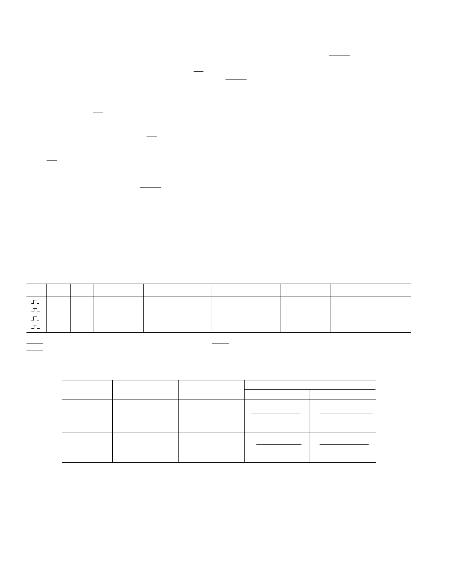
1
Sample tested at +25
°
C to ensure compliance. All input signals are specified with tr = tf = 5 ns (10% to 90% of 5 V) and timed from a voltage level of 1.6 V.
2
See Figures 1 to 6.
3
CLKIN duty cycle range is 20% to 80%. CLKIN must be supplied whenever the AD7703 is not in SLEEP mode. If no clock is present in this case, the device can
draw higher current than specified and possibly become uncalibrated.
4
The AD7703 is production tested with f
CLKIN
at 4.096 MHz. It is guaranteed by characterization to operate at 200 kHz.
5
Specified using 10% and 90% points on waveform of interest.
6
In order to synchronize several AD7703s together using the SLEEP pin, this specification must be met.
7
t
4
and t
13
are measured with the load circuit of Figure 1 and defined as the time required for an output to cross 0.8 V or 2.4 V.
8
t
9
, t
10
, t
15
and t
16
are derived from the measured time taken by the data outputs to change 0.5 V when loaded with the circuit of Figure 1. The measured number is
then extrapolated back to remove the effects of charging or discharging the 100 pF capacitor. This means that the tune quoted in the Timing Characteristics is the
true bus relinquish time of the part and as such is independent of external bus loading capacitances.
9
If CS is returned high before all 20 bits are output, the SDATA and SCLK outputs will complete the current data bit and then go to high impedance.
10
If CS is activated asynchronously to DRDY, CS will not be recognized if it occurs when DRDY is high for four clock cycles. The propagation delay time may be as
great as 4 CLKIN cycles plus 160 ns. To guarantee proper clocking of SDATA when using asynchronous CS, the SCLK input should not be taken high sooner than
4 CLKIN cycles plus 160 ns after CS goes low.
11
SDATA is clocked out on the falling edge of the SCLK input.
CAL
SC1, SC2
SC1,SC2 VALID
t
1
t
2
Figure 2. Calibration Control Timing
CLKIN
SLEEP
t
3
Figure 3. Sleep Mode Timing
I
OL
1.6mA
+2.1V
TO
OUTPUT
PIN
C
L
100pF
I
OH
200µA
Figure 1. Load Circuit for Access Time and Bus Relinquish
Time
AD7703
REV. D
5
DATA
VALID
t
15
HI-Z
SDATA
CS
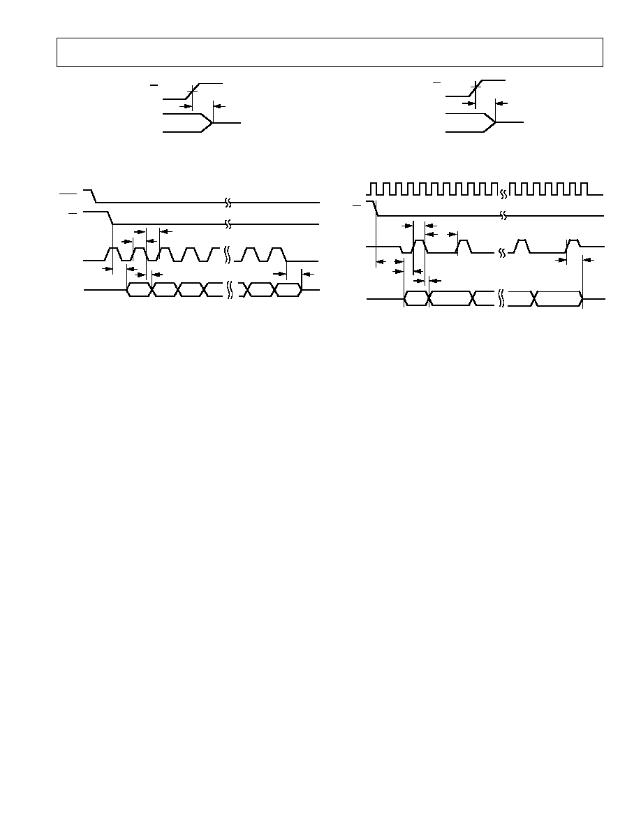
Figure 5a. SEC Mode Data Hold Time
HI-Z
DB19
DB18
DB1
DB0
HI-Z
SCLK
SDATA
CLKIN
CS
HI-Z
t
7
t
8
t
5
t
9
t
4
t
8
HI-Z
Figure 6. SSC Mode Timing Diagram
DATA
VALID
t
10
HI-Z
SDATA
CS
Figure 4. SSC Mode Data Hold Time
HI-Z
DB18
DB1
DB0
HI-Z
SDATA
DRDY
CS
t
12
t
11
t
13
t
14
SCLK
t
16
DB19
Figure 5b. SEC Mode Timing Diagram
TERMINOLOGY
LINEARITY ERROR
This is the maximum deviation of any code from a straight line
passing through the endpoints of the transfer function. The end-
points of the transfer function are zero-scale (not to be confused
with bipolar zero), a point 0.5 LSB below the first code transi-
tion (000 . . . 000 to 000 . . . 001) and full scale, a point 1.5 LSB
above the last code transition (111 . . . 110 to 111 . . . 111).
The error is expressed as a percentage of full scale.
DIFFERENTIAL LINEARITY ERROR
This is the difference between any code's actual width and the
ideal (1 LSB) width. Differential linearity error is expressed in
LSBs. A differential linearity specification of
±
1 LSB or less
guarantees monotonicity.
POSITIVE FULL-SCALE ERROR
Positive full-scale error is the deviation of the last code transition
(111 . . . 110 to 111 . . . 111) from the ideal (V
REF
3/2 LSBs).
It applies to both positive and negative analog input ranges.
UNIPOLAR OFFSET ERROR
Unipolar offset error is the deviation of the first code transition
from the ideal (AGND + 0.5 LSB) when operating in the uni-
polar mode.
BIPOLAR ZERO ERROR
This is the deviation of the midscale transition (0111 . . . 111 to
1000 . . . 000) from the ideal (AGND 0.5 LSB) when operat-
ing in the bipolar mode.
BIPOLAR NEGATIVE FULL-SCALE ERROR
This is the deviation of the first code transition from the ideal
(V
REF
+ 0.5 LSB), when operating in the bipolar mode.
POSITIVE FULL-SCALE OVERRANGE
Positive full-scale overrange is the amount of overhead available
to handle input voltages greater than +V
REF
(for example, noise
peaks or excess voltages due to system gain errors in system cali-
bration routines) without introducing errors due to overloading
the analog modulator or overflowing the digital filter.
NEGATIVE FULL-SCALE OVERRANGE
This is the amount of overhead available to handle voltages be-
low V
REF
without overloading the analog modulator or over-
flowing the digital filter. Note that the analog input will accept
negative voltage peaks even in the unipolar mode.
OFFSET CALIBRATION RANGE
In the system calibration modes (SC2 Low) the AD7703 cali-
brates its offset with respect to the A
IN
pin. The offset calibra-
tion range specification defines the range of voltages that the
AD7701 can accept and still calibrate offset accurately.
FULL-SCALE CALIBRATION RANGE
This is the range of voltages that the AD7703 can accept in the
system calibration mode and still calibrate full scale correctly.
INPUT SPAN
In system calibration schemes, two voltages applied in sequence
to the AD7703's analog input define the analog input range.
The input span specification defines the minimum and maxi-
mum input voltages from zero to full scale that the AD7703 can
accept and still calibrate gain accurately.
AD7703
6
REV. D
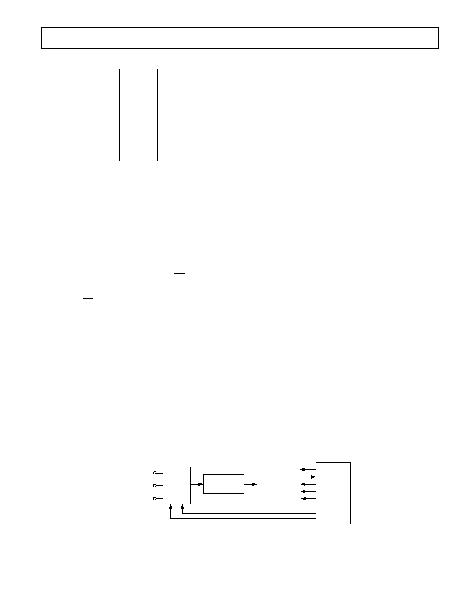
PIN FUNCTION DESCRIPTION
Pin
Mnemonic
Description
1
MODE
Selects the Serial Interface Mode. If MODE is tied to DGND, the Synchronous External Clocking (SEC)
mode is selected. SCLK is configured as an input, and the output appears without formatting, the MSB com-
ing first. If MODE is tied to +5 V, the AD7703 operates in the Synchronous Self-Clocking (SSC) mode.
SCLK is configured as an output, with a clock frequency for f
CLKIN
/4 and 25% duty cycle.
2
CLKOUT
Clock Output to generate an Internal Master Clock by connecting a crystal between CLKOUT and CLKIN.
If an external clock is used, CLKOUT is not connected.
3
CLKIN
Clock Input for External Clock.
4, 17
SC1, SC2
System Calibration Pins. The state of these pins, when CAL is taken high, determines the type of calibration
performed.
5
DGND
Digital Ground. Ground reference for all digital signals.
6
DV
SS
Digital Negative Supply, 5 V nominal.
7
AV
SS
Analog Negative Supply, 5 V nominal.
8
AGND
Analog Ground. Ground reference for all analog signals.
9
A
IN
Analog Input.
10
V
REF
Voltage Reference Input, +2.5 V nominal. This determines the value of positive full-scale in the unipolar
mode and of both positive and negative full-scale in the Bipolar Mode.
11
SLEEP
Sleep mode pin. When this pin is taken low, the AD7703 goes into a low-power mode with typically 10
µ
W
power consumption.
12
BP/UP
Bipolar/Unipolar mode pin. When this pin is Low, the AD7703 is configured for a unipolar input range going
from AGND to V
REF
. When Pin 12 is High, the AD7703 is configured for a bipolar input range,
±
V
REF
.
13
CAL
Calibration mode pin. When CAL is taken High for more than 4 cycles, the AD7703 is reset and performs a
calibration cycle when CAL is brought Low again. The CAL pin can also be used as a strobe to synchronize
the operation of several AD7703s.
14
AV
DD
Analog Positive Supply, +5 V nominal.
15
DV
DD
Digital Positive Supply, +5 V nominal.
16
CS
Chip Select Input. When CS is brought low, the AD7703 will begin to transmit serial data in a format deter-
mined by the state of the MODE pin.
18
DRDY
Data Ready Output. DRDY is low when valid data is available in the output register. It goes high after trans-
mission of a word is completed. It also goes high for four clock cycles when a new data word is being loaded
into the output register, to indicate that valid data is not available, irrespective of whether data transmission is
complete or not.
19
SCLK
Serial Clock Input/Output. The SCLK pin in configured as an input or output, dependent on the type of se-
rial data transmission that has been selected by the MODE pin. When configured as an output in the Syn-
chronous Self-Clocking mode, it has a frequency of f
CLKIN
/4 and a duty cycle of 25%.
20
SDATA
Serial Data Output. The AD7703's output data is available at this pin as a 20-bit serial word.
Table I. Bit Weight Table (2.5 V Reference Voltage)
UNIPOLAR MODE
BIPOLAR MODE
V
LSBs
% FS
ppm FS LSBs
% FS
ppm FS
0.596
0.25
0.0000238
0.24
0.13
0.0000119
0.12
1.192
0.5
0.0000477
0.48
0.26
0.0000238
0.24
2.384
1.00
0.0000954
0.95
0.5
0.0000477
0.48
4.768
2.00
0.0001907
1.91
1.00
0.0000954
0.95
9.537
4.00
0.0003814
3.81
2.00
0.0001907
1.91
PIN CONFIGURATION
DIP, Cerdip, SOIC
MODE
SC1
DGND
CLKOUT
CLKIN
AGND
DV
SS
AV
SS
A
IN
V
REF
SDATA
SCLK
SC2
CAL
AV
DD
DV
DD
DRDY
CS
BP/UP
SLEEP
TOP VIEW
(Not to Scale)
AD7703
1
2
3
4
5
6
7
8
9
10
14
13
12
11
20
19
18
17
16
15
AD7703
REV. D
7
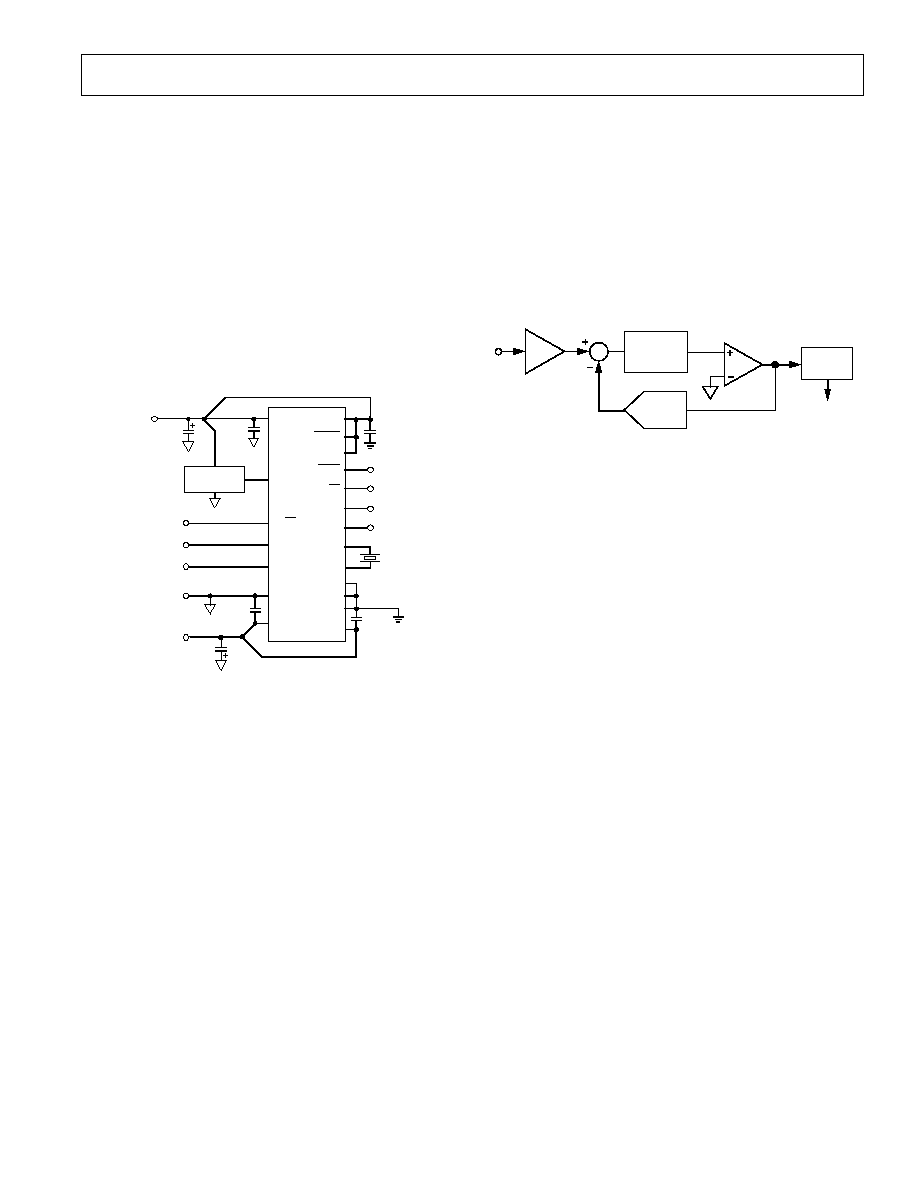
THEORY OF OPERATION
The general block diagram of a sigma-delta ADC is shown in
Figure 8. It contains the following elements:
1. A sample-hold amplifier
2. A differential amplifier or subtracter
3. An analog low-pass filter
4. A 1-bit A/D converter (comparator)
5. A 1-bit DAC
6. A digital low-pass filter
ANALOG
LOW-PASS
FILTER
COMPARATOR
DIGITAL
FILTER
DIGITAL DATA
S/H AMP
DAC
Figure 8. General Sigma-Delta ADC
In operation, the sampled analog signal is fed to the subtracter,
along with the output of the 1-bit DAC. The filtered difference
signal is fed to the comparator, whose output samples the
difference signal at a frequency many times that of the analog
signal frequency (oversampling).
Oversampling is fundamental to the operation of sigma-delta
ADCs. Using the quantization noise formula for an ADC:
SNR
=
(6.02
×
number of bits
+
1.76) dB,
a 1-bit ADC or comparator yields an SNR of 7.78 dB.
The AD7703 samples the input signal at 16 kHz, which spreads
the quantization noise from 0 kHz to 8 kHz. Since the specified
analog input bandwidth of the AD7703 is only 0 Hz to 10 Hz,
the noise energy in this bandwidth would be only 1/800 of the
total quantization noise, assuming that the noise energy was
spread evenly throughout the spectrum. It is reduced still
further by analog filtering in the modulator loop, which shapes
the quantization noise spectrum to move most of the noise
energy to frequencies above 10 Hz. The SNR performance in
the 0 Hz to 10 Hz range is conditioned to the 20-bit level in this
fashion.
The output of the comparator provides the digital input for the
1-bit DAC, so the system functions as a negative feedback loop
which minimizes the difference signal. The digital data that
represents the analog input voltage is in the duty cycle of the
pulse train appearing at the output of the comparator. It can be
retrieved as a parallel binary data word using a digital filter.
Sigma-delta ADCs are generally described by the order of the
analog low-pass filter. A simple example of a first order sigma-
delta ADC is shown in Figure 8. This contains only a first-order
low-pass filter or integrator.
The AD7703 uses a second-order sigma-delta modulator and a
digital filter that provides a rolling average of the sampled
output. After power-up or if there is a step change in the input
voltage, there is a settling time before valid data is obtained.
GENERAL DESCRIPTION
The AD7703 is a 20-bit A/D converter with on-chip digital
filtering, intended for the measurement of wide dynamic range,
low frequency signals such as those representing chemical,
physical or biological processes. It contains a charge-balancing
(sigma-delta) ADC, calibration microcontroller with on-chip
static RAM, a clock oscillator and a serial communications port.
The analog input signal to the AD7703 is continuously sampled
at a rate determined by the frequency of the master clock,
CLKIN. A charge-balancing A/D converter (sigma-delta modu-
lator) converts the sampled signal into a digital pulse train
whose duty cycle contains the digital information. A six-pole
Gaussian digital low-pass filter processes the output of the
sigma-delta modulator and updates the 20-bit output register at
a 4 kHz rate. The output data can be read from the serial port
randomly or periodically at any rate up to 4 kHz.
AD7703
MODE
SDATA
SC1
DGND
CLKOUT
CLKIN
AGND
SCLK
SC2
CAL
CS
BP/UP
DV
SS
DV
DD
SLEEP
RANGE
SELECT
CALIBRATE
ANALOG
INPUT
ANALOG
GROUND
5V
ANALOG
SUPPLY
0.1
µ
F
SERIAL
DATA
SERIAL
CLOCK
READ
(TRANSMIT)
DATA
READY
+5V
ANALOG
SUPPLY
2.5V
0.1
µ
F
0.1
µ
F
DRDY
0.1
µ
F
10
µ
F
AV
DD
V
REF
A
IN
AV
SS
VOLTAGE
REFERENCE
10
µ
F
Figure 7. Typical System Connection Diagram
The AD7703 can perform self-calibration using the on-chip
calibration microcontroller and SRAM to store calibration
parameters. A calibration cycle may be initiated at any time
using the CAL control input.
Other system components may also be included in the
calibration loop to remove offset and gain errors in the input
channel.
For battery operation, the AD7703 also offers a standby mode
that reduces idle power consumption to typically 10
µ
W.
AD7703
8
REV. D
DIGITAL FILTERING
The AD7703's digital filter behaves like an analog filter, with a
few minor differences.
First, since digital filtering occurs after the A to D conversion
process, it can remove noise injected during the conversion
process. Analog filtering cannot do this.
On the other hand, analog filtering can remove noise superim-
posed on the analog signal before it reaches the ADC. Digital
filtering cannot do this and noise peaks riding on signals near
full scale have the potential to saturate the analog modulator
and digital filter, even though the average value of the signal is
within limits. To alleviate this problem, the AD7703 has over-
range headroom built into the sigma-delta modulator and digital
filter which allows overrange excursions of 100 mV. If noise sig-
nals are larger than this, consideration should be given to analog
input filtering, or to reducing the gain in the input channel so
that a full-scale input (2.5 V) gives only a half-scale input to the
AD7703 (1.25 V). This will provide an overrange capability
greater than 100% at the expense of reducing the dynamic range
by 1 bit (50%).
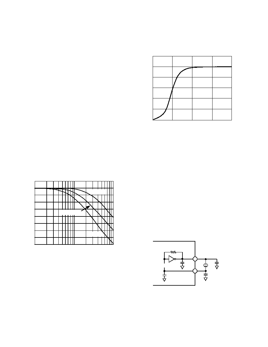
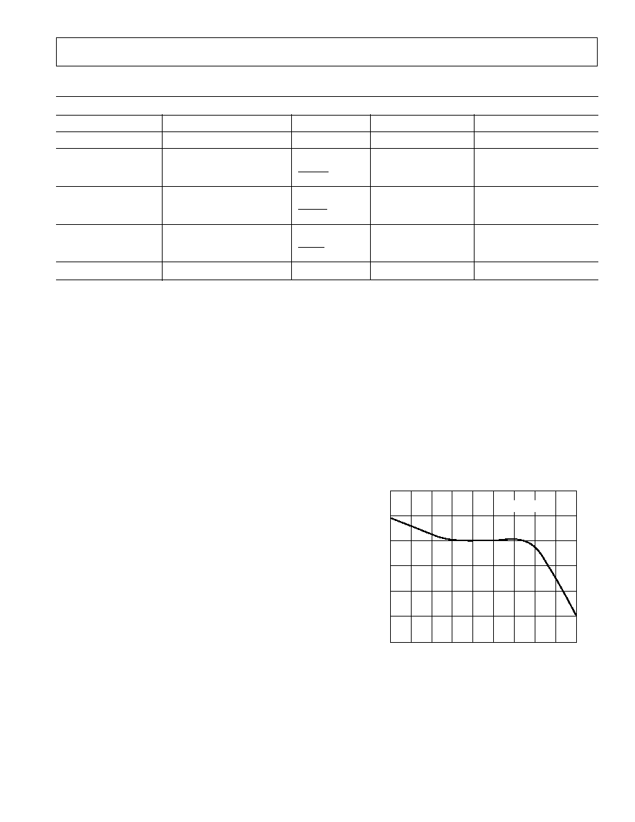
FILTER CHARACTERISTICS
The cutoff frequency of the digital filter is f
CLK
/409600. At the
maximum clock frequency of 4.096 MHz, the cutoff frequency
of the filter is 10 Hz and the data update rate is 4 kHz.
Figure 9 shows the filter frequency response. This is a 6-pole
Gaussian response that provides 55 dB of 60 Hz rejection for a
10 Hz cutoff frequency. If the clock frequency is halved to give a
5 Hz cutoff, 60 Hz rejection is better than 90 dB.
1
10
100
FREQUENCY Hz
20
0
20
40
60
80
100
120
140
160
GAIN dB
f
CLK
= 1MHz
f
CLK
= 2MHz
f
CLK
= 4MHz
Figure 9. Frequency Response of AD7703 Filter
Since the AD7703 contains this low-pass filtering, there is a set-
tling time associated with step function inputs, and data will be
invalid after a step change until the settling time has elapsed.
The AD7703 is, therefore, unsuitable for high speed multiplex-
ing, where channels are switched and converted sequentially at
high rates, as switching between channels can cause a step
change in the input. However, slow multiplexing of the AD7703
is possible, provided that the settling time is allowed to elapse
before data for the new channel is accessed.
The output settling of the AD7703 in response to a step input
change is shown in Figure 10. The Gaussian response has fast
settling with no overshoot, and the worst-case settling time to
±
0.0007% is 125 ms with a 4.096 MHz master clock frequency.
PERCENT OF FINAL VALUE
100
80
60
40
20
0
0
40
80
120
160
TIME ms
Figure 10. AD7703 Step Response
USING THE AD7703
SYSTEM DESIGN CONSIDERATIONS
The AD7703 operates differently from successive approxima-
tion ADCs or integrating ADCs. Since it samples the signal con-
tinuously, like a tracking ADC, there is no need for a start convert
command. The 20-bit output register is updated at a 4 kHz rate,
and the output can be read at any time, either synchronously or
asynchronously.
CLOCKING
The AD7703 requires a master clock input, which may be an
external TTL/CMOS compatible clock signal applied to the
CLKIN pin (CLKOUT not used). Alternatively, a crystal of the
correct frequency can be connected between CLKIN and
CLKOUT, when the clock circuit will function as a crystal
controlled oscillator.
Figure 11 shows a simple model of the on-chip gate oscillator
and Table II gives some typical capacitor values to be used with
various resonators.
AD7703
C2*
C1*
R1
5M
X1
2
3
10pF
10pF
g
m
= 1500
µ
MHO
*SEE TABLE II
Figure 11. On-Chip Gate Oscillator
AD7703
REV. D
9
Table II. Resonator Loading Capacitors
Resonators
C1
C2
Ceramic
200 kHz
330 pF
470 pF
455 kHz
100 pF
100 pF
1.0 MHz
50 pF
50 pF
2.0 MHz
20 pF
20 pF
Crystals
2.000 MHz
30 pF
30 pF
3.579 MHz
20 pF
20 pF
4.096 MHz
None
None
The input sampling frequency, output data rate, filter character-
istics and calibration time are all directly related to the master
clock frequency f
CLKIN
by the ratios given in the specification
table under Dynamic Performance. Therefore, the first step in
system design with the AD7703 is to select a master clock fre-
quency suitable for the bandwidth and output data rate required
by the application.
ANALOG INPUT RANGES
The AD7703 performs conversion relative to an externally sup-
plied reference voltage, which allows easy interfacing to ratio-
metric systems. In addition, either unipolar or bipolar input
voltage ranges may be selected using the BP/UP input. With
BP/UP tied low, the input range is unipolar and the span is
(V
REF
V
AGND
), where V
AGND
is the voltage at the device AGND
pin. With BP/UP tied high, the input range is bipolar and the
span is 2 V
REF
. In the bipolar mode both positive and negative
full scale are directly determined by V
REF
. This offers superior
tracking of positive and negative full scale and better midscale
(bipolar zero) stability than bipolar schemes that simply scale
and offset the input range.
The digital output coding for the unipolar range is unipolar
binary and for the bipolar range it is offset binary. Bit weights
for the unipolar and bipolar modes are shown in Table I.
ACCURACY
Sigma-delta ADCs, like VFCs and other integrating ADCs, do
not contain any source of nonmonotonicity and inherently offer
no missing codes performance.
The AD7703 achieves excellent linearity by the use of high
quality, on-chip silicon dioxide capacitors, which have a very
SYSTEM
REF HI
A
IN
SYSTEM
REF LO
ANALOG
MUX
A0
A1
SIGNAL
CONDITIONING
AD7703
SCLK
SDATA
CAL
SC1
SC2
MICRO
COMPUTER
A
IN
Figure 12. Typical Connections for System Calibration
low capacitance/voltage coefficient. The device also achieves low
input drift through the use of chopper-stabilized techniques in
its input stage. To ensure excellent performance over time and
temperature, the AD7703 uses digital calibration techniques
which minimize offset and gain error to typically
±
4 LSBs.
AUTOCALIBRATION
The AD7703 offers both self-calibration and system-calibration
facilities. For calibration to occur, the on-chip microcontroller
must record the modulator output for two different input condi-
tions. These are the "zero scale" and "full scale" points. In uni-
polar self-calibration mode, the zero scale point is V
AGND
and
the full-scale point is V
REF
. With these readings the microcon-
troller can calculate the gain slope for the input to output trans-
fer function of the converter. In unipolar mode the slope factor
is determined by dividing the span between zero and full scale
by 2
20
. In bipolar mode it is determined by dividing the span by
2
19
since the inputs applied represent only half the total codes.
In both unipolar and bipolar modes the slope factor is saved and
used to calculate the binary output code when an analog input is
applied to the device. Table IV gives the output code size after
calibration.
System calibration allows the AD7703 to compensate for system
gain and offset errors. A typical circuit where this might be used
is shown in Figure 12.
System calibration performs the same slope factor calculations
as self-calibration but uses voltage values presented by the
system to the A
IN
pin for the zero and full-scale points. There
are two system calibration modes.
The first mode offers system level calibration for system offset
and system gain. This is a two step operation. The zero-scale
point must be presented to the converter first. It must be
applied to the converter before the calibration step is initiated
and remain stable until the step is complete. The DRDY output
from the device will signal when the step is complete by going
low. After the zero-scale point is calibrated the full-scale point is
applied and the second calibration step is initiated. Again the
voltage must remain stable throughout the calibration step.
The two step calibration mode offers another feature. After the
sequence has been completed, additional offset calibrations can
be performed by themselves to adjust the zero reference point to
a new system zero reference value. This second system
calibration mode uses an input voltage for the zero-scale
calibration point but uses the V
REF
value for the full-scale point.
AD7703
10
REV. D
Initiating Calibration
Table III illustrates the calibration modes available in the
AD7703. Not shown in the table is the function of the BP/UP
pin which determines whether the converter has been calibrated
to measure bipolar or unipolar signals. A calibration step is
initiated by bringing the CAL pin high for at least 4 CLKIN
cycles and then bringing it low again. The states of SC1 and
SC2 along with the BP/UP pin will determine the type of
calibration to be performed. All three signals should be stable
before the CAL pin is taken positive. The SC1 and SC2 inputs
are latched when CAL goes high. The BP/UP input is not
latched and therefore must remain in a fixed state throughout
the calibration and measurement cycles. Any time the state of
the BP/UP is changed, a new calibration cycle must be
performed to enable the AD7703 to function properly in the
new mode.
When a calibration step is initiated, the DRDY signal will go
high and remain high until the step is finished. Table III shows
the number of clock cycles each calibration requires. Once a
calibration step is initiated it must finish before a new calibra-
tion step can be executed. In the two step system calibration
mode, the offset calibration step must be initiated before initiat-
ing the gain calibration step.
Table IV. Output Code Size After Calibration
1 LSB
CAL MODE
ZERO-SCALE
GAIN FACTOR
UNIPOLAR
BIPOLAR
Self-Cal
V
AGND
V
REF
(V
REF
V
AGND
)
1048576
2(V
REF
V
AGND
)
1048576
System Cal
S
OFF
S
GAIN
(S
GAIN
S
OFF
)
1048576
2(S
GAIN
S
OFF
)
1048576
Table III. Calibration Truth Table
CAL
SC1
SC2
CAL TYPE
ZERO-SCALE CAL FULL-SCALE CAL SEQUENCE
CALIBRATION TIME
0
0
Self-Cal
V
AGND
V
REF
One Step
3,145,655 Clock Cycles
1
1
System Offset
A
IN
_
1st Step
1,052,599 Clock Cycles
0
1
System Gain
_
A
IN
2nd Step
1,068,813 Clock Cycles
1
0
System Offset
A
IN
V
REF
One Step
2,117,389 Clock Cycles
NOTE
DRDY
remains high throughout the calibration sequence. In the Self-Cal mode, DRDY falls once the AD7703 has settled to the analog input. In all other modes
DRDY
falls as the device begins to settle.
When self-calibration is completed, DRDY falls and the output
port is updated with a data word that represents the analog
input signal. When a system calibration step is completed,
DRDY
will fall and the output port will be updated with the
appropriate data value (all 0s for the zero-scale point and all 1s
for the full-scale point). In the system calibration mode, the
digital filter must settle before the output code will represent the
value of the analog input signal. Tables IV and V indicate the
output code size and output coding of the AD7703 in its
various modes. In these tables, S
OFF
is the measured system
offset in volts and S
GAIN
is the measured system gain at the
full-scale point in volts.
Span and Offset Limits
Whenever a system calibration mode is used, there are limits on
the amount of offset and span which can be accommodated.
The range of input span in both the unipolar and bipolar modes
has a minimum value of 0.8 V
REF
and a maximum value of
2 (V
REF
+ 0.1 V).
The amount of offset which can be accommodated depends on
whether the unipolar or bipolar mode is being used. In unipolar
mode, the system calibration modes can handle a maximum
offset of 0.2 V
REF
and a minimum offset of (V
REF
+ 0.1 V).
Thus the AD7703 in the unipolar mode can be calibrated to
mimic bipolar operation.
AD7703
REV. D
11
Table V. AD7703 Output Coding
I
NPUT VOLTAGE, UNIPOLAR MODE INPUT VOLTAGE, BIPOLAR MODE
System Cal
Self Cal
Output Codes
Self-Cal
System Cal
>(
S
GAIN
1.5 LSB)
>
(V
REF
1.5 LSB)
FFFFF
>
(V
REF
1.5 LSB)
>
(S
GAIN
1.5 LSB)
S
GAIN
1.5 LSB
V
REF
1.5 LSB
FFFFF
FFFFE
V
REF
1.5 LSB
S
GAIN
1.5 LSB
(S
GAIN
S
OFF
)/2 0.5 LSB
(V
REF
V
AGND
)/2 0.5 LSB
80000
7FFFF
V
AGND
0.5 LSB
S
OFF
0.5 LSB
S
OFF
+ 0.5 LSB
V
AGND
+ 0.5 LSB
00001
00000
V
REF
+ 0.5 LSB
S
GAIN
+ 2 S
OFF
+ 0.5 LSB
<
(S
OFF
+ 0.5 LSB)
<
(V
AGND
+ 0.5 LSB)
00000
<
(V
REF
+ 0.5 LSB)
<(S
GAIN
+2 S
OFF
+ 0.5 LSB)
updated at a rate determined by the master clock, therefore the
amount of offset drift which occurs will be proportional to the
elapsed time between samples. Thus, to minimize offset drift at
higher temperatures, higher CLKIN rates are recommended.
Gain drift within the converter depends mainly upon the tem-
perature tracking of the internal capacitors. It is not affected by
leakage currents so that it is significantly less than offset drift.
The typical gain drift of the AD7703 is less than 40 LSBs over
the specified temperature range.
Measurement errors due to offset drift or gain drift can be elimi-
nated at any time by recalibrating the converter. Using the sys-
tem calibration mode can also minimize offset and gain errors in
the signal conditioning circuitry. Integral and differential linear-
ity are not significantly affected by temperature changes.
BIPOLAR OFFSET LSBs
160
0
80
160
240
320
55
5
25
105
125
TEMPERATURE
°
C
80
35
15
45
65
85
CLKIN = 4.096MHz
Figure 13. Typical Bipolar Offset vs. Temperature after
Calibration at +25
°
C
In the bipolar mode the system offset calibration range is
restricted to
±
0.4 V
REF
. It should be noted that the span
restrictions limit the amount of offset which can be calibrated.
The span range of the converter in bipolar mode is equidistant
around the voltage used for the zero scale point. When the zero-
scale point is calibrated it must not cause either of the two
endpoints of the bipolar transfer function to exceed the positive
or the negative input overrange points (+V
REF
+ 0.1) V or
V
REF
+ 0.1) V. If the span range is set to a minimum (0.8 V
REF
)
the offset voltage can move +0.4 V
REF
without causing the end
points of the transfer function to exceed the overrange points.
Alternatively, if the span range is set to 2 V
REF
, the input offset
cannot move more than +0.1 V or 0.1 V before an endpoint of
the transfer function exceeds the input overrange limit.
POWER-UP AND CALIBRATION
A calibration cycle must be carried out after power-up to
initialize the device to a consistent starting condition and correct
calibration. The CAL pin must be held high for at least four
clock cycles, after which calibration is initiated on the falling
edge of CAL and takes a maximum of 3,145,655 clock cycles
(approximately 768 ms with a 4.096 MHz clock). See Table III.
The type of calibration cycle initiated by CAL is determined by
the SC1 and SC2 inputs, in accordance with Table III.
Drift Considerations
The AD7703 uses chopper stabilization techniques to minimize
input offset drift. Charge injection in the analog switches and
leakage currents at the sampling node are the primary sources of
offset voltage drift in the converter. Figure 13 indicates the typi-
cal offset due to temperature changes after calibration at 25
°
C.
Drift is relatively flat up to 75
°
C. Above this temperature, leak-
age current becomes the main source of offset drift. Since leak-
age current doubles approximately every 10
°
C, the offset drifts
accordingly. The value of the voltage on the sample capacitor is
AD7703
12
REV. D
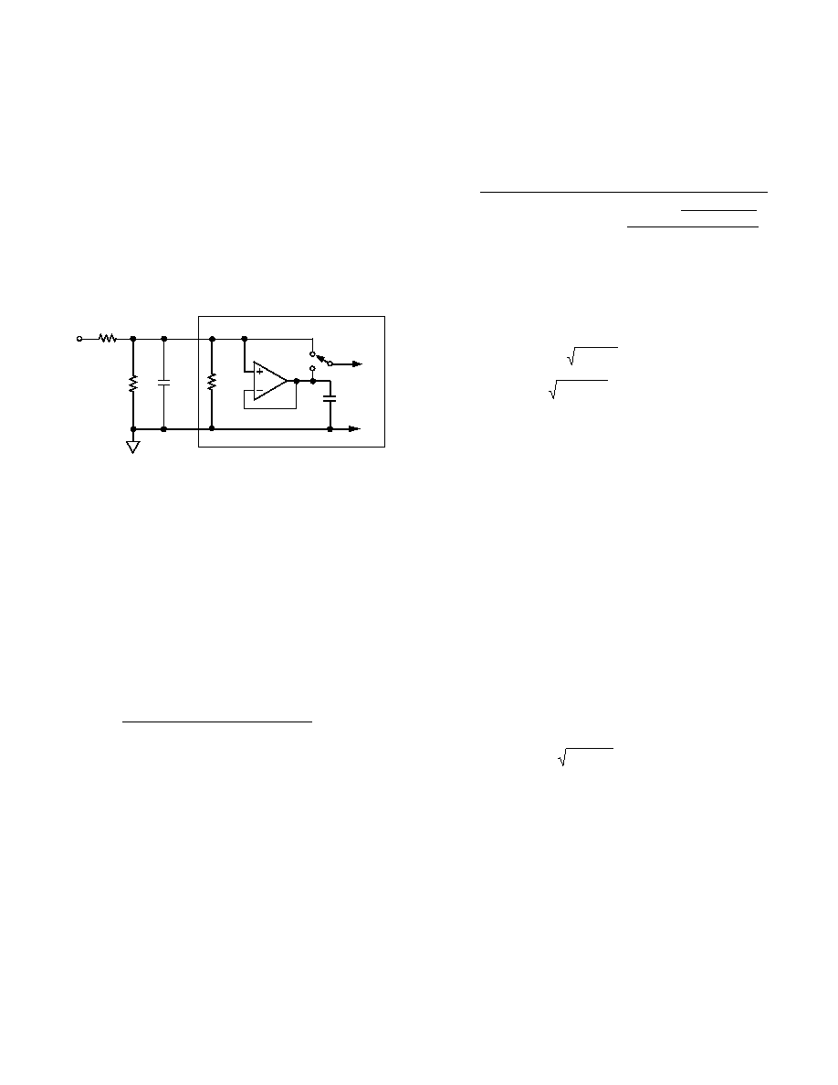
INPUT SIGNAL CONDITIONING
Reference voltages from +1 V to +3 V may be used with the
AD7703, with little degradation in performance. Input ranges
that cannot be accommodated by this range of reference voltages
may be achieved by input signal conditioning. This may take the
form of gain to accommodate a smaller signal range, or passive
attenuation to reduce a larger input voltage range.
Source Resistance
If passive attenuators are used in front of the AD7703, care
must be taken to ensure that the source impedance is suffi-
ciently low. The dc input resistance for the AD7703 is over
1 G
. In parallel with this there as a small dynamic load which
varies with the clock frequency (see Figure 14). Each time the
A
IN
R1
R2
C
EXT
AGND
AD7703
V
OS
100mV
C
IN
10pF
V
IN
1G
Figure 14. Equivalent Input Circuit and Input Attenuator
analog input is sampled, a 10 pF capacitor draws a charge
packet of maximum 1 pC (10 pF 100 mV) from the analog
source with a frequency f
CLKIN
/256. For a 4.096 MHz CLKIN,
this yields an average current draw of 16 nA. After each sample
the AD7703 allows 62 clock periods for the input voltage to
settle. The equation which defines settling time is:
V
O
=
V
IN
[1 e
t /RC
]
where V
O
, is the final settled value, V
IN
, is the value of the input
signal, R is the value of the input source resistance, C is the
10 pF sample capacitor. The value of t is equal to 62/f
CLKIN
.
The following equation can be developed which gives the max-
imum allowable source resistance, R
S(MAX)
for an error of V
E
.
R
S(MAX )
=
62
f
CLKIN
·(10 pF )· ln (100 mV /V
E
)
Provided the source resistance is less than this value, the analog
input will settle within the desired error band in the requisite 62
clock periods. Insufficient settling leads to offset errors. These
can be calibrated in system calibration schemes.
If a limit of 600 nV (0.25 LSB at 20 bits) is set for the maxi-
mum offset voltage, then the maximum allowable source resis-
tance is 125 k
from the above equation, assuming that there is
no external stray capacitance.
An RC filter may be added in front of the AD7703 to reduce
high frequency noise. With an external capacitor added from
A
IN
to AGND, the following equation will specify the maximum
allowable source resistance:
R
S(MAX )
=
62
f
CLKIN
·(C
IN
+
C
EXT
) · ln
100 mV ·
C
IN
(C
IN
+
C
EXT
)
V
E
The practical limit to the maximum value of source resistance is
thermal (Johnson) noise. A practical resistor may be modeled as
an ideal (noiseless) resistor in series with a noise voltage source
or in parallel with a noise current source.
V
n
=
4 kTRf Volts
i
n
=
4 kTf / R Amperes
where k is Boltzmann's constant (1.38 10
23
J/K), and T is
temperature in degrees Kelvin (
°
C + 273).
Active signal conditioning circuits such as op amps generally do
not suffer from problems of high source impedance. Their open
loop output resistance is normally only tens of ohms and, in any
case, most modern general purpose op amps have sufficiently
fast closed loop settling time for this not to be a problem. Offset
voltage in op amps can be eliminated in a system calibration
routine.
Antialias Considerations
The digital filter of the AD7703 does not provide any rejection
at integer multiples of the sampling frequency (nf
CLKIN
/256,
where n = 1, 2, 3 . . . ).
With a 4.096 MHz master clock there are narrow (
±
10 Hz)
bands at 16 kHz, 32 kHz, 48 kHz, etc., where noise passes
unattenuated to the output.
However, due to the AD7703's high oversampling ratio of 800
(16 kHz to 20 Hz) these bands occupy only a small fraction of
the spectrum, and most broadband noise is filtered.
The reduction in broadband noise is given by:
e
out
=
e
in
2 f
C
/ f
S
=
0.035 e
in
where e
in
and e
out
are rms noise terms referred to the input and f
C
is the filter 3 dB corner frequency (f
CLKIN
/409600) and f
S
is the
sampling frequency (f
CLKIN
/256).
Since the ratio of f
S
to f
CLKIN
is fixed, the digital filter reduces
broadband white noise by 96.5% independent of the master
clock frequency.

AD7703
REV. D
13
Therefore, the two analog supplies should be individually
decoupled to AGND using 100 nF ceramic capacitors to
provide power supply noise rejection at these frequencies. The
two digital supplies should similarly be decoupled to DGND.
The positive digital supply (DV
DD
) must never exceed the
positive analog supply (AV
DD
) by more than 0.3 V. Power
supply sequencing is therefore important. If separate analog and
digital supplies are used, care must be taken to ensure that the
analog supply is powered up first.
It is also important that power is applied to the AD7703 before
signals at V
REF
, A
IN
or the logic input pins in order to avoid any
possibility of latch-up. If separate supplies are used for the
AD7703 and the system digital circuitry, then the AD7703
should be powered up first.
A typical scheme for powering the AD7703 from a single set of
±
5 V rails is shown Figure 7. In this circuit AV
DD
and DV
DD
are
brought along separate tracks from the same +5 V supply.
Thus, there is no possibility of the digital supply coming up
before the analog supply.
SLEEP MODE
The low power standby mode is initiated by taking the SLEEP
input low, which shuts down all analog and digital circuits and
reduces power consumption to 10
µ
W. When coming out of
SLEEP mode it is sometimes possible (when using a crystal to
generate CLKIN, for example) to lose the calibration coeffi-
cients. Therefore, it is advisable as a safeguard to always do a
calibration cycle after coming out of SLEEP mode.
DIGITAL INTERFACE
The AD7703's serial communications port allows easy
interfacing to industry standard microprocessors. Two different
modes of operation are available, optimized for different types
of interface.
VOLTAGE REFERENCE CONNECTIONS
The voltage applied to the V
REF
pin defines the analog input
range. The specified reference voltage is 2.5 V, but the AD7703
will operate with reference voltages from 1 V to 3 V with little
degradation in performance.
The reference input presents exactly the same dynamic load as
the analog input, but in the case of the reference input, source
resistance and long settling time introduce gain errors rather
than offset errors. Fortunately, most precision references have
sufficiently low output impedance and wide enough bandwidth
to settle to the required accuracy within 62 clock cycles.
The digital filter of the AD7703 removes noise from the refer-
ence input, just as it does with noise at the analog input, and
the same limitations apply regarding lack of noise rejection at
integer multiples of the sampling frequency. Note that the refer-
ence should be chosen to minimize noise below 10 Hz. The
AD7703 typically exhibits 1.6 LSB rms noise in its measure-
ments. This specification assumes a clean reference. Many
monolithic bandgap references are available which can supply
the 2.5 V needed for the AD7703. However, some of these are
not specified for noise especially in the 0.1 Hz to 10 Hz band-
width. If the reference noise in this bandwidth is excessive, it
can degrade the performance of the AD7703. Recommended
references are the AD580 and the LT1019. Both of these 2.5 V
references typically have less than 10 V p-p noise in the 0.1 Hz
to 10 Hz band.
POWER SUPPLIES AND GROUNDING
AGND is the ground reference voltage for the AD7703, and is
completely independent of DGND. Any noise riding on the
AGND input with respect to the system analog ground will
cause conversion errors. AGND should therefore be used as the
system ground and also as the ground for the analog input and
the reference voltage.
The analog and digital power supplies to the AD7703 are
independent and separately pinned out, to minimize coupling
between analog and digital sections of the device. The digital
filter will provide rejection of broadband noise on the power
supplies, except at integer multiples of the sampling frequency.
AD7703
14
REV. D
SYNCHRONOUS SELF-CLOCKING MODE (SSC)
The SSC mode (MODE pin high) allows easy interfacing to
serial-parallel conversion circuits in systems with parallel data
communication. This mode allows interfacing to 74XX299
Universal Shift registers without any additional decoding. The
SSC mode can also be used with microprocessors such as the
68HC11 and 68HC05, which allow an external device to clock
their serial port.
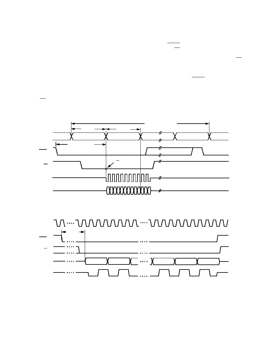
Figure 15 shows the timing diagram for the SSC mode. Data is
clocked out by an internally generated serial clock. The
AD7703 divides each sampling interval into sixteen distinct
periods. Eight periods of 64 clock pulses are for analog settling
and eight periods of 64 clock pulses are for digital computation.
The status of CS is polled at the beginning of each digital
computation period. If it is low at any of these times, then
SCLK will become active and the data word currently in the
output register will be transmitted, MSB first. After the LSB has
been transmitted DRDY will go high until the new data word
becomes available. If CS, having been brought low, is taken
high again at any time during data transmission, SDATA and
SCLK will go three-state after the current bit finishes. If CS is
subsequently brought low, transmission will resume with the
next bit during the subsequent digital computation period. If
transmission has not been initiated and completed by the time
the next data word is available, DRDY will go high for four
clock cycles then low again as the new word is loaded into the
output register.
A more detailed diagram of the data transmission in the SSC
mode is shown in Figure 16. Data bits change on the falling
edge of SCLK and are valid on the rising edge of SCLK.
ANALOG TIME 0
DIGITAL TIME 7
SCLK (O)
SDATA (O)
HI-Z
HI-Z
HI-Z
HI-Z
MSB
DRDY (O)
DIGITAL TIME 0
CS POLLED
CS (I)
INTERNAL
STATUS
72 CLKIN CYCLES
64 CLKIN
CYCLES
64 CLKIN
CYCLES
1024 CLKIN CYCLES
LSB
Figure 15. Timing Diagram for SSC Data Transmission Mode
CLKIN (I)
DRDY (O)
SDATA (O)
DB19 (MSB)
DB18
DB2
DB1
DB0 (LSB)
HI-Z
HI-Z
SCLK (O)
HI-Z
HI-Z
CS (I)
72
CLKIN
CYCLES
DB17
Figure 16. SSC Mode Showing Data Timing Relative to SCLK
AD7703
REV. D
15
SYNCHRONOUS EXTERNAL CLOCK MODE (SEC)
The SEC mode (MODE pin grounded) is designed for direct
interface to the synchronous serial ports of industry standard
microprocessors such as the 68HC11 and 68HC05. The SEC
mode also allows customized interfaces, using I/O port pins, to
microprocessors that do not have a direct fit with the AD7703's
other mode.
As shown in Figure 17, a falling edge on CS enables the serial
data output with the MSB initially valid. Subsequent data bits
change on the falling edge of an externally supplied SCLK.
After the LSB has been transmitted, DRDY and SDATA go
three-state. If CS is low and the AD7703 is still transmitting
data when a new data word becomes available, the old data
word continues to be transmitted and the new data is lost.
If CS is taken high at any time during data transmission,
SDATA will go three-state immediately. If CS returns low, the
AD7703 will continue transmission with the same data bit. If
transmission has not been initiated and completed by the time
the next data word becomes available, and if CS is high, DRDY
will return high for four clock cycles, then fall as the new word is
loaded into the output register.
DIGITAL NOISE AND OUTPUT LOADING
As mentioned earlier, the AD7703 divides its internal timing
into two distinct phases, analog sampling and settling and digital
computation. In the SSC mode, data is transmitted only during
the digital computation periods, to minimize the effects of
digital noise on analog performance. In the SEC mode data
transmission is externally controlled, so this automatic safeguard
does not exist. To compensate, the AD7703 should be
synchronized to the digital system clock via CLKIN when used
in the SEC mode.
Whatever mode of operation is used, resistive and capacitive
loads on digital outputs should be minimized in order to reduce
crosstalk between analog and digital portions of the circuit. For
this reason connection to low-power CMOS logic such as one of
the 4000 series or 74C families is recommended.
DRDY (O)
SDATA (O)
DB19 (MSB)
DB18
DB2
DB1
DB0 (LSB)
HI-Z
SCLK (O)
HI-Z
CS (I)
DB17
Figure 17. Timing Diagram for the SEC Mode
AD7703
16
REV. D
C1477b29/96
PRINTED IN U.S.A.
MECHANICAL INFORMATION
Dimensions shown in inches and (mm)
20-Pin Plastic DIP (Suffix N)
20-Pin Cerdip (Suffix Q)
20-Lead SOIC (Suffix R)