Äîêóìåíòàöèÿ è îïèñàíèÿ www.docs.chipfind.ru
REV. A
Information furnished by Analog Devices is believed to be accurate and
reliable. However, no responsibility is assumed by Analog Devices for its
use, nor for any infringements of patents or other rights of third parties
which may result from its use. No license is granted by implication or
otherwise under any patent or patent rights of Analog Devices.
a
16-Bit
DSP DACPORT
AD766
One Technology Way, P.O. Box 9106, Norwood, MA 02062-9106, U.S.A.
Tel: 617/329-4700
Fax: 617/326-8703
FEATURES
Zero-Chip Interface to Digital Signal Processors
Complete DACPORT®
On-Chip Voltage Reference
Voltage and Current Outputs
Serial, Twos-Complement Input
3 V Output
Sample Rates to 390 kSPS
94 dB Minimum Signal-to-Noise Ratio
81 dB Maximum Total Harmonic Distortion
15-Bit Monotonicity
5 V to 12 V Operation
16-Pin Plastic and Ceramic Packages
Available in Commercial, Industrial, and Military
Temperature Ranges
APPLICATIONS
Digital Signal Processing
Noise Cancellation
Radar Jamming
Automatic Test Equipment
Precision Industrial Equipment
Waveform Generation
PRODUCT DESCRIPTION
The AD766 16-bit DSP DACPORT provides a direct, three-
wire interface to the serial ports of popular DSP processors, in-
cluding the ADSP-2101, TMS320CXX, and DSP56001. No
additional "glue logic" is required. The AD766 is also com-
plete, offering on-chip serial-to-parallel input format conver-
sion, a 16-bit current-steering DAC, voltage reference, and a
voltage output op amp. The AD766 is fabricated in Analog
Devices' BiMOS II mixed-signal process which provides bipolar
transistors, MOS transistors, and thin-film resistors for preci-
sion analog circuits in addition to CMOS devices for logic.
The design and layout of the AD766 have been optimized for ac
performance and are responsible for its guaranteed and tested
94 dB signal-to-noise ratio to 20 kHz and 79 dB SNR to
250 kHz. Laser-trimming the AD766's silicon chromium thin-
film resistors reduces total harmonic distortion below 81 dB
(at 1 kHz), a specification also production tested. An optional
linearity trim pin allows elimination of midscale differential
linearity error for even lower THD with small signals.
The AD766's output amplifier provides a
±
3 V signal with a
high slew rate, small glitch, and fast settling. The output ampli-
fier is short circuit protected and can withstand indefinite shorts
to ground.
DACPORT is a registered trademark of Analog Devices, Inc.
The serial interface consists of bit clock, data, and latch enable
inputs. The twos-complement data word is clocked MSB first
on falling clock edges into the serial-to-parallel converter, con-
sistent with the serial protocols of popular DSP processors. The
input clock can support data transfers up to 12.5 MHz. The
falling edge of latch enable updates the internal DAC input reg-
ister at the sample rate with the sixteen bits most recently
clocked into the serial input register.
The AD766 operates over a
±
5 V to
±
12 V power supply range.
The digital supplies, +V
L
and V
L
, can be separated from the
analog signal supplies, +V
S
and V
S
, for reduced digital
crosstalk. Separate analog and digital ground pins are also pro-
vided. An internal bandgap reference provides a precision volt-
age source to the output amp that is stable over temperature and
time.
Power dissipation is typically 120 mW with
±
5 V supplies and
300 mW with
±
12 V. The AD766 is available in commercial
(0
°
C to +70
°
C), industrial (40
°
C to +85
°
C), and military
(55
°
C to +125
°
C) grades. Commercial and industrial grade
parts are available in a 16-pin plastic DIP; military parts pro-
cessed to MIL-STD-883B are packaged in a 16-pin ceramic
DIP. See Analog Devices' Military Products Databook or current
military data sheet for specifications for the military version.
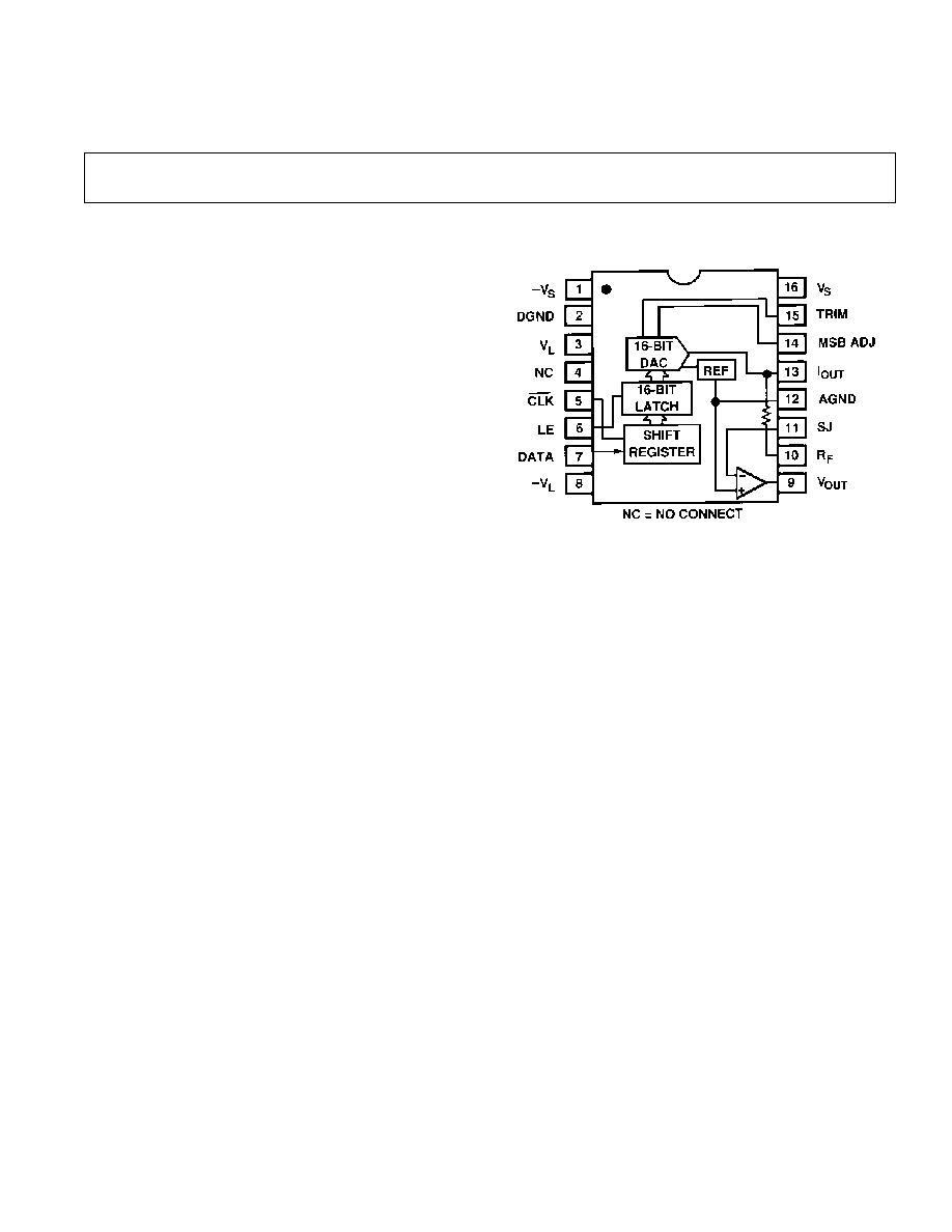
FUNCTIONAL BLOCK DIAGRAM

REV. A
2
AD766SPECIFICATIONS
AD766J
AD766A
Parameter
Min
Typ
Max
Min
Typ
Max
Units
RESOLUTION
16
16
Bits
DIGITAL INPUTS
V
IH
2.0
+V
L
2.0
+V
L
V
V
IL
0.8
0.8
V
I
IH
, V
IH
= V
L
1.0
1.0
µ
A
I
IL
, V
IL
= 0.4
10
10
µ
A
SERIAL PORT TIMING
Serial Clock Period (t
CLK
)
95
115
ns
Serial Clock HI (t
HI
)
30
30
ns
Serial Clock LO (t
LO
)
30
70
ns
Data Valid (t
DATA
)
40
40
ns
Data Setup (t
S
)
15
20
ns
Data Hold (t
H
)
15
20
ns
Clock-to-Latch-Enable (t
CTLE
)
80
100
ns
Latch-Enable-to-Clock (t
LETC
)
15
15
ns
Latch Enable HI (t
LEHI
)
40
40
ns
Latch Enable LO (t
LELO
)
40
80
ns
ACCURACY
1
Gain Error
±
2.0
±
2.0
% of FSR
Gain Drift
±
25
±
25
ppm of FSR/
°
C
Midscale Output Voltage Error
±
30
±
30
mV
Bipolar Zero Drift
±
4
±
4
ppm of FSR/
°
C
Differential Linearity Error
±
0.001
±
0.001
% of FSR
Monotonicity
15
15
Bits
TOTAL HARMONIC DISTORTION
F
OU T
= 1037 Hz
1
0 dB
88
81
88
81
dB
20 dB
75
65
75
65
dB
60 dB
37
27
37
27
dB
F
OUT
= 49.07 kHz
2
0 dB
77
72
77
72
dB
20 dB
69
66
69
66
dB
60 dB
25
21
25
21
dB
SIGNAL-TO-NOISE RATIO
3
20 Hz to 20 kHz (F
OUT
= 1037 Hz)
1
94
102
94
102
dB
20 kHz to 250 kHz (F
OUT
= 49.07 kHz)
2
79
83
79
83
dB
SETTLING TIME (to
±
0.0015% of FSR)
Voltage Output
1
6 V Step
1.5
1.5
µ
s
1 LSB Step
1.0
1.0
µ
s
Slew Rate
9
9
V/
µ
s
Current Output
1 mA Step 10
to 100
Load
350
350
ns
1 k
Load
350
350
ns
OUTPUT
Voltage Output Configuration
1
Bipolar Range
±
2.88
±
3.0
±
3.12
±
2.88
±
3.0
±
3.12
V
Output Current
±
8.0
±
8.0
mA
Output Impedance
0.1
0.1
Short Circuit Duration
Indefinite to Common
Indefinite to Common
Current Output Configuration
Bipolar Range
±
0.7
±
1.0
±
1.3
±
0.7
±
1.0
±
1.3
mA
Output Impedance (
±
30%)
1.7
1.7
k
POWER SUPPLY
Voltage: +V
L
and +V
S
4.75
13.2
4.75
13.2
V
Voltage:
V
L
and V
S
13.2
4.75
13.2
4.75
V
Current Case 1
1
: V
S
and V
L
= +5 V
+I
12.0
15.0
12.0
15.0
mA
Current Case 1
1
:
V
S
and V
L
= 5 V
I
12.0
15.0
12.0
15.0
mA
Current
Case 2:
1
V
S
and V
L
= +12 V
+I
10.5
10.5
mA
Current Case 2:
1
V
S
and V
L
= 12 V
I
14
14
mA
Current
Case 3
4
: V
S
and V
L
= +5 V
+I
12
12
mA
Current Case 2:
1
V
S
and V
L
= 12 V
I
14
14
mA
Power Dissipation: V
S
and V
L
=
±
5 V
1
120
150
120
150
mW
Power Dissipation:
V
S
and V
L
=
±
12 V
300
300
mW
Power Dissipation:
V
S
and V
L
= +5 V,
Power Dissipation:
V
S
and V
L
= 12 V
4
225
225
mW
(T
MIN
to T
MAX
, 5 V supplies, F
S
= 500 kSPS unless otherwise noted. No deglitchers or
MSB trimming is used.)
AD766
REV. A
3
WARNING!
ESD SENSITIVE DEVICE
ESD SENSITIVITY
The AD766 features input protection circuitry consisting of large "distributed" diodes and
polysilicon series resistors to dissipate both high energy discharges (Human Body Model) and
fast, low energy pulses (Charged Device Model). Per Method 3015.2 of MIL-STD-883C, the
AD766 has been classified as a Category 1 Device.
Proper ESD precautions are strongly recommended to avoid functional damage or perfor-
mance degradation. Charges as high as 4000 volts readily accumulate on the human body and
test equipment, and discharge without detection. Unused devices must be stored in conduc-
tive foam or shunts, and the foam discharged to the destination socket before devices are
removed. For further information on ESD precaution, refer to Analog Devices' ESD
Prevention Manual.
ABSOLUTE MAXIMUM RATINGS*
V
L
to DGND . . . . . . . . . . . . . . . . . . . . . . . . . . . . . . 0 to 13.2 V
V
S
to AGND . . . . . . . . . . . . . . . . . . . . . . . . . . . . . . 0 to 13.2 V
V
L
to DGND . . . . . . . . . . . . . . . . . . . . . . . . . . 13.2 V to 0 V
V
S
to AGND . . . . . . . . . . . . . . . . . . . . . . . . . . 13.2 V to 0 V
Digital Inputs to DGND . . . . . . . . . . . . . . . . . . . . 0.3 V to V
L
AGND to DGND . . . . . . . . . . . . . . . . . . . . . . . . . . . . .
±
0.3 V
Short Circuit Protection . . . . . . . . Indefinite Short to Ground
Soldering . . . . . . . . . . . . . . . . . . . . . . . . . . . . . +300
°
C, 10 sec
*Stresses greater than those listed under "Absolute Maximum Ratings" may cause
permanent damage to the device. This is a stress rating only and functional
operation of the device at these or any other conditions above those indicated in
the operational section of this specification is not implied. Exposure to absolute
maximum rating conditions for extended periods may affect device reliability.
PIN DESIGNATIONS
Pin
Function
Description
1
V
S
Analog Negative Power Supply
2
DGND
Digital Ground
3
V
L
Logic Positive Power Supply
4
NC
No Connection
5
CLK
Clock Input
6
LE
Latch Enable Input
7
DATA
Serial Data Input
8
V
L
Logic Negative Power Supply
9
V
OUT
Voltage Output
10
R
F
Feedback Resistor
11
SJ
Summing Junction
12
AGND
Analog Ground
13
I
OUT
Current Output
14
MSB ADJ
MSB Adjustment Terminal
15
TRIM
MSB Trimming Potentiometer Terminal
16
V
S
Analog Positive Power Supply
ORDERING GUIDE
Temperature
Package
Model
Range
Option*
AD766JN
0
°
C to +70
°
C
N-16
AD766AN
40
°
C to +85
°
C
N-16
AD766SD/883B 55
°
C to +125
°
C
D-16
*N = Plastic DIP; D = Ceramic DIP.
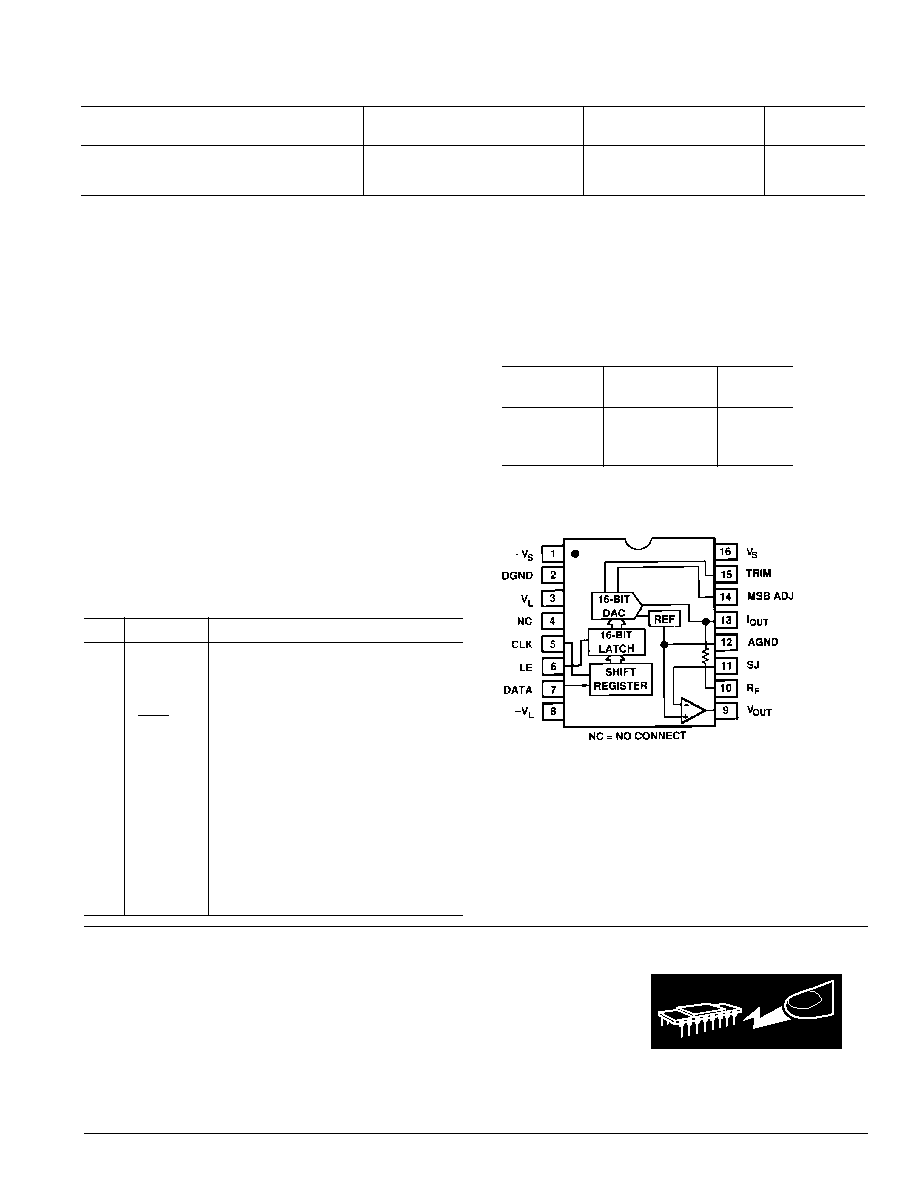
CONNECTION DIAGRAM
AD766J
AD766A
Parameter
Min
Typ
Max
Min
Typ
Max
Units
TEMPERATURE RANGE
Specified
0
+70
40
+85
°
C
Storage
60
+100
60
+100
°
C
NOTES
1
For A grade only, voltage outputs are guaranteed only if +V
S
7 V and V
S
7 V.
2
Specified using external op amp, see Figure 3 for more details.
3
Tested at full-scale input.
4
For A grade only, power supplies must be symmetric, i.e., V
S
= |V
S
| and +V
L
= |
V
L
|
. Each supply must independently meet this equality within
±
5%.
All min and max specifications are guaranteed. Specifications in boldface are tested on all production units at final electrical test. Results from those tests are used to
calculate outgoing quality levels.
Specifications subject to change without notice.
AD766Definition of Specifications
4
REV. A
TOTAL HARMONIC DISTORTION
Total Harmonic Distortion (THD) is defined as the ratio of the
square root of the sum of the squares of the values of the har-
monics to the value of the fundamental input frequency. It is ex-
pressed in percent (%) or decibels (dB).
THD is a measure of the magnitude and distribution of integral
linearity error and differential linearity error. The distribution of
these errors may be different, depending on the amplitude of the
output signal. Therefore, to be most useful, THD should be
specified for both large and small signal amplitudes.
SETTLING TIME
Settling Time is the time required for the output to reach and
remain within a specified error band about its final value, mea-
sured from the digital input transition. It is the primary measure
of dynamic performance.
BIPOLAR ZERO ERROR
Bipolar Zero Error or midscale error is the deviation of the ac-
tual analog output from the ideal output (0 V) when the 2s
complement input code representing half scale (all 0s) is loaded
in the input register.
DIFFERENTIAL LINEARITY ERROR
Differential Linearity Error is the measure of the variation in
analog value, normalized to full scale, associated with a 1 LSB
change in the digital input. Monotonic behavior requires that
the differential linearity error not exceed 1 LSB in the negative
direction.
MONOTONICITY
A D/A converter is monotonic if the output either increases or
remains constant as the digital input increases.
SIGNAL-TO-NOISE RATIO
SNR is defined as the ratio of the fundamental to the square
root of the sum of the squares for the values of all the nonfun-
damental, nonharmonic signals for a specified bandwidth. SNR
is tested at full-scale input. The AD766 specifies SNR for
20 kHz and 250 kHz bandwidths.
FUNCTIONAL DESCRIPTION
Serial input data is clocked into the AD766's shift register by
the falling edge of CLK. Data is presumed to be in twos
complement format with MSB (i.e., the sign bit) clocked in first.
The shift register converts the most recently clocked-in 16 bits
to a parallel word. The falling edge of the latch enable (LE) sig-
nal causes the most recent parallel word to be transferred to the
internal DAC input latch. See Figure 2 for detailed serial port
timing requirements.
The contents of the DAC input latch cause the 16-bit DAC to
generate a corresponding current. This
±
1 mA current is avail-
able directly on the I
OUT
pin.
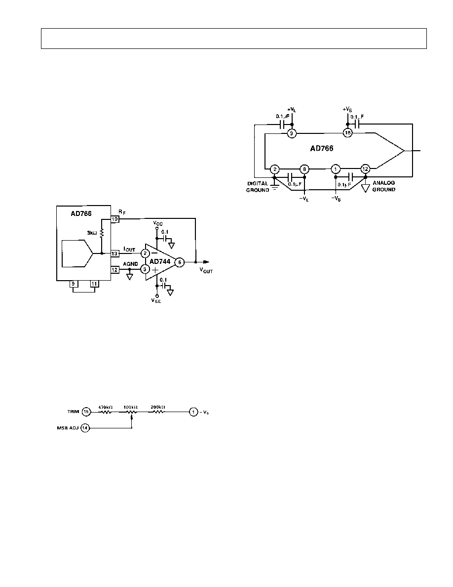
To use the internal op amp, connect I
OUT
(Pin 13) directly to
the summing junction pin, SJ (Pin 11) and connect the feedback
resistor pin, R
F
(Pin 10) to V
OUT
(Pin 9). Note that the internal
op amp is in the inverting configuration. Using the internal
3 k
feedback resistor, this op amp will produce
±
3 V outputs.
One advantage of external pins at each end of the feedback
resistor is that it allows the user to implement a single pole
active low-pass filter simply by adding a capacitor across these
pins (Pins 10 and 13). The circuit can best be understood
redrawn as shown in Figure 1.
Figure 1. Low-Pass Filter Using External Capacitor
The frequency response from this filter will be
V
OUT
(s)
I
OUT
=
-
R
F
R
F
·
C
·
s
+
1
where R
F
is 3 k
(
±
20%).
Figure 2. AD766 Serial Input Timing
5
REV. A
The digital ground pin returns ground current from the digital
logic portions of the AD766 circuitry. This pin should be con-
nected to the digital common point in the system.
As illustrated in Figure 5, the analog and digital grounds should
be connected together at one point in the system.
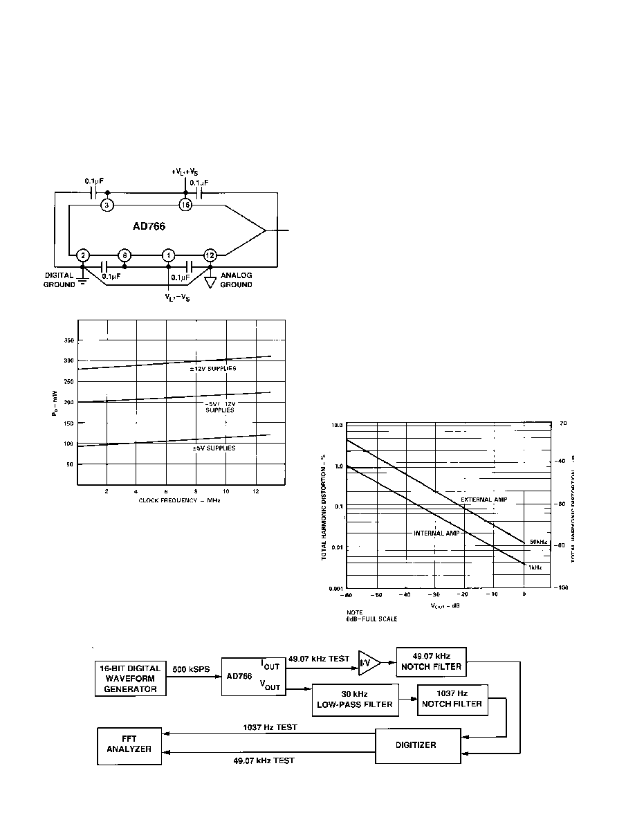
Figure 5. Recommended Circuit Schematic
POWER SUPPLIES AND DECOUPLING
The AD766 has four power supply input pins.
±
V
S
provide the
supply voltages to operate the linear portions of the DAC in-
cluding the voltage reference, output amplifier and control am-
plifier. The
±
V
S
supplies are designed to operate from
±
5 V to
±
12 V.
The
±
V
L
supplies operate the digital portions of the chip, in-
cluding the input shift register and the input latching circuitry.
The
±
V
L
supplies are also designed to operate from
±
5 V to
±
12 V. To assure freedom from latch-up, V
L
should never go
more negative than V
S
.
Special restrictions on power supplies apply to extended tem-
perature range versions of the AD766 that do not apply to the
commercial AD766J. First, supplies must be symmetric. That is,
+V
S
= V
S
and +V
L
= V
L
. Each supply must independently
meet this equality within
±
5%. Since we require that V
S
V
L
to guarantee latch-up immunity, this symmetry principle implies
that the positive analog supply must be greater than or equal to
the positive digital supply, i.e., V
S
V
L
for extended-temper-
ature range parts. In other words, the digital supply range must
be inside the analog supply range. Second, the internal op amp's
performance in generating voltage outputs is only guaranteed if
+V
S
7 V (and V
S
7 V, by the symmetry principle). These
constraints do not apply to the AD766J.
Decoupling capacitors should be used on all power supply pins.
Furthermore, good engineering practice suggests that these ca-
pacitors be placed as close as possible to the package pins as
well as the common points. The logic supplies,
±
V
L
, should be
decoupled to digital common; and the analog supplies,
±
V
S
,
should be decoupled to analog common.
The use of four separate power supplies will reduce feedthrough
from the digital portion of the system to the linear portions of
the system, thus contributing to the performance as tested.
However, four separate voltage supplies are not necessary for
good circuit performance. For example, Figure 6 illustrates a
For applications requiring broader bandwidths and/or even
lower noise than that afforded by the AD766's internal op amp,
an external op amp can easily by used in its place. I
OUT
(Pin 13)
drives the negative (inverting) input terminal of the external op
amp, and its external voltage output is connected to the feed-
back resistor pin, R
F
(Pin 10). To insure that the AD766's un-
used internal op amp remains in a closed-loop configuration,
V
OUT
(Pin 9) should be tied to the summing junction pin, SJ
(Pin 11).
As an example, Figure 3 shows the AD766 using the AD744 op
amp as an external current-to-voltage converter. In this invert-
ing configuration, the AD744 will provide the same
±
3 V out-
put as the internal op amp would have. Other recommended
amplifiers include the AD845 and AD846. Note that a single
pole of low-pass filtering could also be attained with this circuit
simply by adding a capacitor in parallel with the feedback resis-
tor as just shown in Figure 1.
Figure 3. External Op Amp Connections
Residual DAC differential linearity error around midscale can
be externally trimmed out, improving THD beyond the
AD766's guaranteed tested specifications. This error is most
significant with low-amplitude signals because the ratio of the
midscale linearity error to the signal amplitude is greatest in this
case, thereby increasing THD. The MSB adjust circuitry shown
in Figure 4 can be used for improving THD with low-level sig-
nals. Otherwise, the AD766 will operate to its specifications
with MSB ADJ (Pin 14) and TRIM (Pin 15) unconnected.
Figure 4. Optional MSB Adjustment Circuit
ANALOG CIRCUIT CONSIDERATIONS
GROUNDING RECOMMENDATIONS
The AD766 has two ground pins, designated AGND (analog
ground) and DGND (digital ground). The analog ground pin is
the "high-quality" ground reference point for the device. The
analog ground pin should be connected to the analog common
point in the system. The output load should also be connected
to that same point.
Analog Circuit ConsiderationsAD766
AD766
REV. A
6
system where only a single positive and a single negative supply
are available. In this case, the positive logic and positive analog
supplies may both be connected to the single positive supply.
The negative logic and negative analog supplies may both be
connected to the single negative supply. Performance would
benefit from a measure of isolation between the supplies intro-
duced by using simple low-pass filters in the individual power
supply leads.
Figure 6. Alternate Recommended Schematic
Figure 7. Power Dissipation vs. Clock Frequency
As with most linear circuits, changes in the power supplies will
affect the output of the DAC. Analog Devices recommends that
well regulated power supplies with less than 1% ripple be incor-
porated into the design of any system using these device.
MEASUREMENT OF TOTAL HARMONIC DISTORTION
The THD specification of a DSP DAC represents the amount
of undesirable signal produced during reconstruction of a digital
waveform. To account for the variety of operating conditions
Figure 8. Distortion Test Circuit
in signal processing applications, the DAC is tested at two
output frequencies and at three signal levels over the full oper-
ating temperature ranges.
A block diagram of the test setup is shown in Figure 8. In this
test setup, a digital data stream, representing a 0 dB, 20 dB or
60 dB sine wave is sent to the device under test. The frequen-
cies used are 1037 Hz and 49.07 kHz. Input data is latched into
the AD766 at 500 kSPS. The AD766 under test produces an
analog output signal using the on-board op amp for 1 kHz and
an external op amp for 50 kHz.
The automatic test equipment digitizes the output test wave-
form, and then an FFT to 250 kHz is performed on the results
of the test. Based on the first 9 harmonics of the fundamental
1037 Hz and the first 3 harmonics of the 49.07 kHz output
waves, the total harmonic distortion of the device is calculated.
Neither a deglitcher nor an MSB trim is used during the THD
test.
The circuit design, layout and manufacturing techniques em-
ployed in the production of the AD766 result in excellent THD
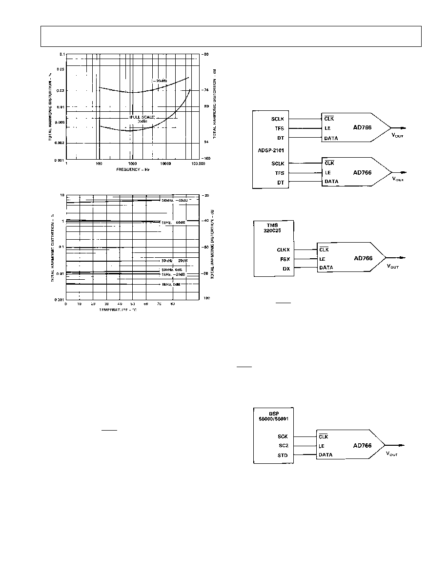
performance. Figure 9 shows the typical unadjusted THD per-
formance of the AD766 for various amplitudes of 1 kHz and
50 kHz sine waves. As can be seen, the AD766 offers excellent
performance even at amplitudes as low as 60 dB. Figure 10
illustrates the typical THD versus frequency performance from
the internal amplifier for a filtered AD766 output. At frequen-
cies greater than approximately 30 kHz, depending on the low-
pass filter used, an improvement in THD of 34 dB over the
performance shown in the figure can be achieved. Figure 11
illustrates the consistent THD performance of the AD766
over temperature.
Figure 9. Typical Unadjusted THD
7
REV. A
ApplicationsAD766
Figure 10. Typical THD vs. Frequency
Figure 11. THD vs. Temperature
INTERFACING THE AD766 TO DIGITAL SIGNAL
PROCESSORS
The AD766 is specifically designed to easily interface to several
popular digital signal processors (DSP) without any additional
logic. Such an interface reduces the possibility of interface prob-
lems and improves system reliability by minimizing component
count.
AD766 TO ADSP-2101
The ADSP-2101 incorporates two complete serial ports which
can be directly interfaced to the AD766 as shown in Figure 12.
The SCLK, TFS and DT outputs of the ADSP-2101 are con-
nected directly to the CLK, LE and DATA inputs of the
AD766, respectively. SCLK is internally generated and can be
programmed to operate from 94 Hz to 6.25 MHz. Data (DT) is
valid on the falling edge of SCLK. After 16 bits have been trans-
mitted, the falling edge of TFS updates the AD766's data latch.
Using both serial ports of the ADSP-2101, two AD766's can be
directly interfaced with no additional hardware.
AD766 TO TMS320C25
Figure 13 shows the zero-chip interface to the TMS320C25.
The interface to other TMS320C2X processors is similar. Note
that the C25 should be run in continuous mode. The C25's
frame synch signal (FSX) will be asserted at the beginning of
each 16-bit word but will actually latch in the previous word.
Figure 12. AD766 to ADSP-2101/ADSP-2102/ ADSP-2105/
ADSP-2111
Figure 13. AD766 to TMS320C25
The CLKS, FSX and DX outputs of the TMS320C25 are con-
nected to the CLK, LE and DATA inputs of the AD766, re-
spectively. Data (DX) is valid on the falling edge of CLKX. The
maximum serial clock rate of the TMS320C25 is 5 MHz.
AD766 TO DSP56000/56001
Figure 14 shows the zero-chip interface to the DSP56000/
56001. The SSI of the 56000/56001 allows serial clock rates up
to fosc/4. SCK, SC2 and STD can be directly connected to the
CLK
, LE and DATA inputs of the AD766. The CRA control
register of the 56000 allows SCK to be internally generated and
software configurable to various divisions of the master clock
frequency. The data (STD) is valid on the falling edge of SCK.
Figure 14. AD766 to DSP56000/DSP56001
AD766
REV. A
8
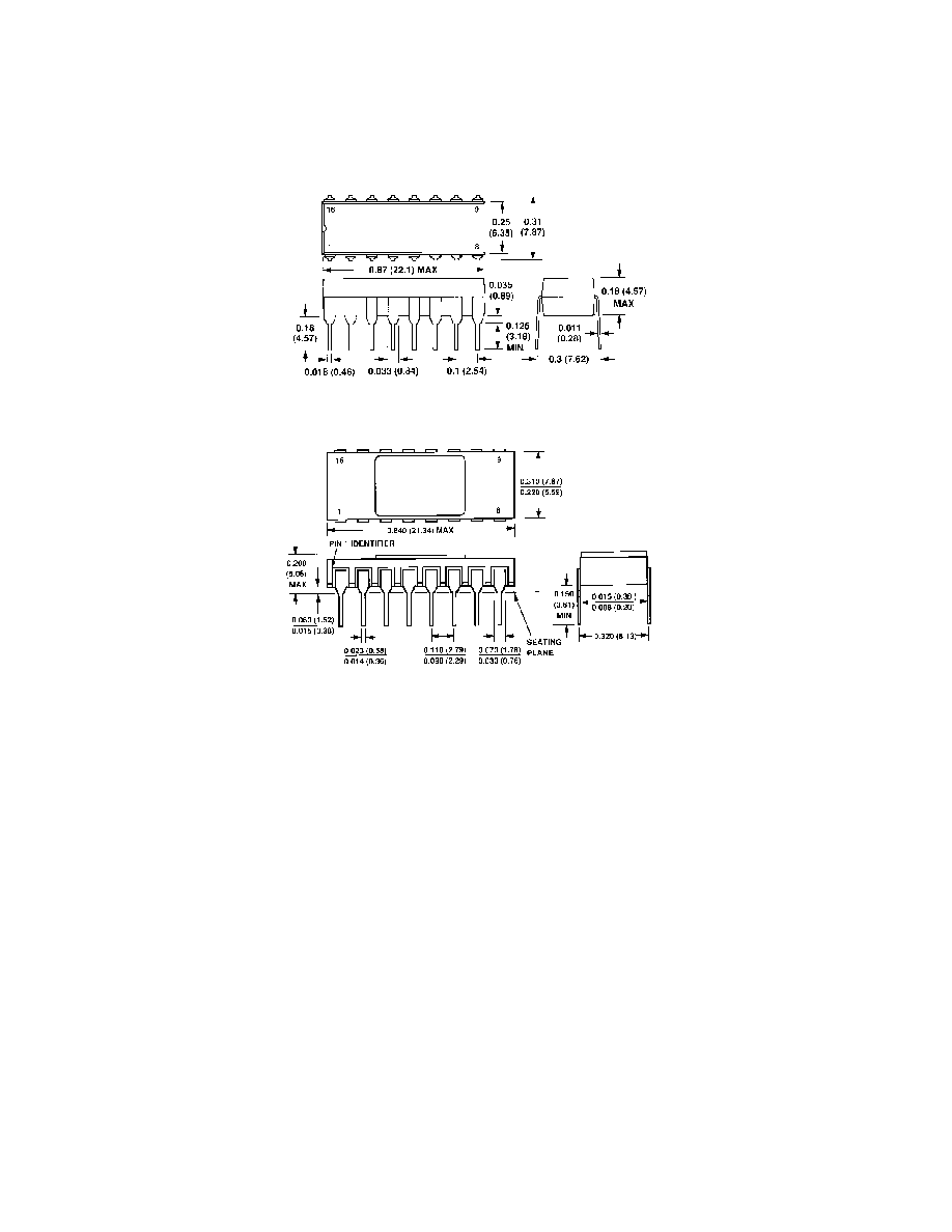
OUTLINE DIMENSIONS
Dimensions shown in inches and (mm).
C1385a163/91
PRINTED IN U.S.A.
16-Pin Plastic DIP (N-16)
D-16
16-Lead Side Brazed Ceramic DIP