Äîêóìåíòàöèÿ è îïèñàíèÿ www.docs.chipfind.ru
One Technology Way, P.O. Box 9106, Norwood. MA 02062-9106, U.S.A.
Tel: 617/329-4700
Fax: 617/326-8703
REV. A
Information furnished by Analog Devices is believed to be accurate and
reliable. However, no responsibility is assumed by Analog Devices for its
use, nor for any infringements of patents or other rights of third parties
which may result from its use. No license is granted by implication or
otherwise under any patent or patent rights of Analog Devices.
=
Evaluation Board for 12-bit high speed,
low power, successive-approximation ADC
EVAL-AD7492CB
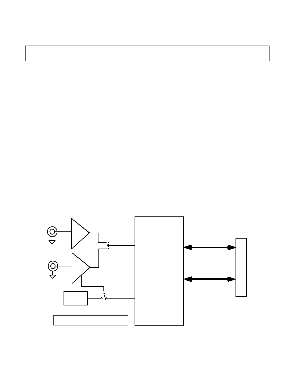
FUNCTIONAL BLOCK DIAGRAM
FEATURES
Full-Featured Evaluation Board for the AD7492
EVAL-CONTROL BRD2 Compatible
Stand Alone Capability
On-Board Analog Buffering and Reference
Optional On-Board Analog Bias-Up Circuit
Various Linking Options
PC Software for Control and Data Analysis when used
with EVAL-CONTROL BRD2
I N T R O D U C T I O N
This Technical Note describes the evaluation board for the
AD7492 12-bit, high speed, low power, internal reference
and clock, successive approximation A/D converter that
operates from a single 2.7 V to 5.25 V supply. Full data on
the AD7492 is available in the AD7492 data sheet available
from Analog Devices and should be consulted in conjunction
with this Technical Note when using the Evaluation Board.
On-board components include an AD780 which is a pin
programmable +2.5 V or +3 V ultra high precision bandgap
reference, two AD797 op-amps used to buffer the analog
input, and an OP07 op-amp used to buffer the DC bias
voltage applied to the optional analog input bias-up circuit.
There are various link options which are explained in detail
on page 2.
Interfacing to this board is through a 96-way connector. This
96-way connector is compatible with the EVAL-CONTROL
BRD2 which is also available from Analog Devices. External
sockets are provided for the
CONVST input and the VIN
inputs.
OPERATING THE AD7492 EVALUATION BOARD
Power Supplies
When using this evaluation board with the EVAL-CON-
TROL BRD2, all supplies are provided from the EVAL-
CONTROL BRD2 through the 96 way connector.
When using the board as a stand alone unit, external supplies
must be provided. This evaluation board has five power
supply inputs: V
DD
, A
GND
, V
SS
, V
DRIVE
and D
GND
. +5 V must
be connected to the V
DD
input to supply the AV
DD
and DV
DD
pins on the AD7492, the AD780 voltage reference, the
positive supply pin of all three op-amps and the digital
control logic. 0 V is connected to the A
GND
input. -5 V must
be connected to the V
SS
input to supply the negative supply
pins on all three op-amps. The V
DRIVE
input can be used to
provide an external voltage for the output drivers on the
AD7492. If an external V
DRIVE
is supplied, it is referenced to
the D
GND
input which should be tied to 0 V. The supplies are
decoupled to the relevant ground plane with 47µF tantalum
and 0.1µF multilayer ceramic capacitors at the point where
they enter the board. The supply pins of the op-amps and
Vin
Unipolar
Ain
Bipolar
Ain
Ref Out
External
Reference
Buffer
Bias-up
buffer
96
P
i
n
E
v
al-
C
ont
r
o
l
Bo
a
rd
I
nt
er
fa
ce
Data Bus
Control Lines
AD7492 ADC
Power Supply Circuit

EVAL-AD7492CB
2
REV. A
reference are also decoupled to A
GND
with a 10µF tantalum and a 0.1µF ceramic capacitor. The AD7492 AV
DD
supply pin is
decoupled to A
GND
with 10uF tantalum and 0.1µF multilayer ceramic capacitors. The AD7492 DV
DD
and VDRIVE pins are
decoupled to A
GND
with 10uF tantalum capacitors and to D
GND
with 0.1µF multilayer ceramic capacitors.
Extensive ground planes are used on this board to minimize the effect of high frequency noise interference. There are two
ground planes, A
GND
and D
GND
. These are connected at one location close to the AD7492.
Analog Input Section
The analog input section of this evaluation board accommodates unipolar and bipolar signals. Unipolar signals within the
AD7492 analog input signal range of 0 V - 2.5 V are connected via SK1. They are then buffered by the on-board buffer before
being applied to the VIN pin of the AD7492. Bipolar signals are connected via SK3 and are biased up by the on-board bias-
up buffer circuit before being applied to the VIN pin of the AD7492. The input impedence of the bias-up circuit is 50
which
is determined by the value of R7. The input impedence may be modified by removing/changing the value of R7. To obtain
optimum performance from this evaluation board the use of an impedence matched, passive filter is recommended before the
analog signal is applied to the evaluation board. For example, when using a 100KHz input tone, a 100KHz 50
filter from
TTE (part number KC5-100K-15K-50/50-720B) is suitable.
R13 Potentiometer (50Kohm)
This variable resistor is used to trim the DC bias voltage applied to the optional analog input bias-up circuit. This bias voltage
is factory preset to 1.25 V which biases a bipolar signal to swing around the midpoint of the analog input range (0 - 2.5 V).
If any adjustment is required, the user can use the histogram window in the eval-board software to analyze the DC voltage
variation while adjusting the trim pot. To view this properly, an analog input signal should not be applied to the board. Under
normal operation this pot should not be adjusted as it is preset for optimum performance.
LINK AND SWITCH OPTIONS
There are 12 link options which must be set for the required operating setup before using the evaluation board. The functions
of these options are outlined below.
Link No.
Function.
LK1
This link is used to select the DC bias voltage to be applied to the optional Vin bias-up circuit.
If the user is using the bias-up circuit, this link must be inserted which will apply the 2.5 V reference voltage
to the bias-up circuit. This causes a bipolar signal (applied to the bipolar vin input socket) to be biased up
around +1.25 V before it is applied to the AD7492 VIN pin. - see also LK10 (below).
When this link is in position "A" the bias-up circuit is supplied by the AD7492 internal reference.
When this link is in position "B" the bias-up circuit is supplied by the AD780 external reference.
If the bias up circuit is not being used this link should be removed.
LK2
This link must be in position "A" if external power supplies are being used. In this position the control logic
is being powered by the voltage applied to the VDD input.
When power is being supplied from the EVAL-CONTROL BRD2, this link can be moved to position "B"
if the user wants to drive the control logic from a separate +5 V which is generated on the EVAL-CONTROL
BRD2.
LK3
This link option selects the sleep mode that the AD7492 can be put into.
When this link is in position "A" the part goes into full sleep when low power operation is selected.
When this link is in position "B" the part goes into partial sleep when low power operation is selected.
LK4
This link option selects the source of the
CONVST input.
When this link is in position "A" the
CONVST input is provided by the EVAL-CONTROL BRD2.
When this link is in position "B" the
CONVST input is provided via the external socket, SK2.
LK5
This link option selects the source of the
RD input.
When this link is in position "A" the
RD input is provided by the EVAL-CONTROL BRD2.
When this link is in position "B" the
RD input is tied to GND.
LK6
This link option selects the source of the
CS input.
When this link is in position "A" the
CS input is provided by the EVAL-CONTROL BRD2.
When this link is in position "B" the
CS input is tied to GND.
LK7
This link option sets the voltage applied to the VDRIVE pin on the AD7492.
When this link is in position "A", VDRIVE is connected directly to the DVDD pin.
When this link is in position "B", an external voltage must be applied to the VDRIVE pin Via J3.
LK8
This link selects the source of the V
DD
supply.
When this link is in position "A" V
DD
must be supplied from an external source via J2.
When this link is in position "B" V
DD
is supplied from the EVAL-CONTROL BRD2.
LK9
This link selects the source of the V
SS
supply.
When this link is in position "A" V
SS
must be supplied from an external source via J2.
When this link is in position "B" V
SS
is supplied from the EVAL-CONTROL BRD2.

EVAL-AD7492CB
REV. A
3
Continued on next page
LK10
This link must be in position "A" if a bipolar AIN signal is being applied to the bipolar Vin socket, SK3.
This link must be in position "B" if a unipolar AIN signal is being applied to the unipolar Vin socket, SK1.
LK11
This link is used to connect in the impedence matching resistor, R5, for unipolar Vin.
LK12
This link is used to connect in the impedence matching resistor, R7, for bipolar Vin.
SET-UP CONDITIONS
Care should be taken before applying power and signals to the evaluation board to ensure that all link positions are as per the
required operating mode. Table I shows the position in which all the links are set when the evaluation board is sent out. All
links are set for use with the EVAL-CONTROL BRD2.
Table I. Initial Link and Switch Positions
Link No.
Position
Function.
LK1
B
Provides DC bias voltage to the analog bias-up circuit using AD780 external reference.
LK2
B
The digital logic circuitry is powered from the EVAL-CONTROL BRD2.
LK3
B
Part goes into partial sleep mode if low power operation selected.
LK4
A
CONVST signal is provided by the EVAL-CONTROL BRD2 via J1.
LK5
A
RD signal is provided by the EVAL-CONTROL BRD2 via J1.
LK6
A
CS signal is provided by the EVAL-CONTROL BRD2 via J1.
LK7
A
AD7492 VDRIVE pin is connected to the AD7492 DVDD pin.
LK8
B
V
DD
is supplied by the EVAL-CONTROL BRD2 via J1.
LK9
B
V
SS
is supplied by the EVAL-CONTROL BRD2 via J1.
LK10
A
The AD7492 Vin pin is connected to the bipolar Vin.
LK11
Inserted
Unipolar Vin impedence matching resistor is connected into circuit.
LK12
Inserted
Bipolar Vin impedence matching resistor is connected into circuit.
EVAL-AD7492CB
4
REV. A
EVAL-CONTROL BRD2 INTERFACING
Interfacing to the EVAL-CONTROL BRD2 is via a 96-way
connector, J1. The pinout for the J1 connector is shown in
Figure 2 and its pin designations are given in Table II.
1
32
1
32
A
B
C
Figure 1. Pin Configuration for the 96-Way
Connector, J1
96-Way Connector Pin Description
D0-D11
Data Bit 0 to Data Bit 11. Three-state TTL
outputs. D11 is the MSB.
+5VD
Digital +5 V supply. This can be used to provide
a separate +5 V supply for the digital logic if
required via LK2.
R D
Read. This is an active low logic input connected
to the
RD pin of the AD7492 via LK5.
C S
Chip Select. This is an active low logic input
connected to the
CS pin of the AD7492 via LK6.
F L 0
Flag zero. This logic input is connected to the
CONVST input of the AD7492 via LK4.
IRQ2
Interrupt Request 2. This is a logic output and is
connected to the BUSY logic output on the
AD7492.
D G N D
Digital Ground. These lines are connected to
the digital ground plane on the evaluation
board. It allows the user to provide the digital
supply via the connector along with the other
digital signals.
A G N D
Analog Ground. These lines are connected to
the analog ground plane on the evaluation
board.
AV
SS
Negative Supply Voltage. This provides a nega-
tive supply to the on-board op-amps via LK9.
AV
DD
Positive Supply Voltage. This provides a positive
supply to the op-amps, the reference, the AD7492
and the digital logic.
When interfacing directly to the EVAL-CONTROL BRD2,
all power supplies and control signals are generated by the
EVAL-CONTROL BRD2. However, due to the nature of
the DSP interface on the EVAL-CONTROL BRD2, AD7492
sampling rates greater than 750 KHz are not supported when
interfacing the EVAL-AD7492CB directly to the EVAL-
CONTROL BRD2.
Table II. 96-Way Connector Pin Functions.
ROW A
ROWB
R O W C
1
2
D 0
3
D 1
4
D G N D
D G N D
D G N D
5
D 2
6
D 3
7
D 4
8
+5VD
+5VD
+5VD
9
R D
D 5
10
D 6
C S
11
D 7
12
D G N D
D G N D
D G N D
13
D 8
14
D 9
15
D10
16
D G N D
D G N D
D G N D
17
F L 0
D11
IRQ2
18
19
20
D G N D
D G N D
D G N D
21
A G N D
A G N D
A G N D
22
A G N D
A G N D
A G N D
23
A G N D
A G N D
A G N D
24
A G N D
A G N D
A G N D
25
A G N D
A G N D
A G N D
26
A G N D
A G N D
A G N D
27
A G N D
28
A G N D
29
A G N D
A G N D
A G N D
30
A G N D
31
AVSS
AVSS
AVSS
32
AVDD
AVDD
AVDD
Note : The unused pins of the 96-way connector are not shown.

EVAL-AD7492CB
REV. A
5
S O C K E T S
There are three input sockets relevant to the operation of the
AD7492 on this evaluation board. The function of these
sockets is outlined in Table III.
Table III. Socket Functions
Socket
Function
SK1
Sub-Miniature BNC Socket for unipolar ana-
log input. Analog inputs in the acceptable
AD7492 analog input range (0 V to REFIN)
are applied to this socket. The signal is then
buffered before it is applied to the AD7492
VIN pin.
SK2
Sub-Miniature BNC Socket for external
CONVST input.
SK3
Sub-Miniature BNC Socket for Bipolar ana-
log input The AD7492 can only accept analog
inputs in the range 0 V to REFIN. Bipolar
analog inputs in the range -1.25 V to +1.25 V
applied to this socket are biased up to the
acceptable AD7492 input range by the on-
board bias-up circuit before being applied to
the AD7492 VIN pin.
C O N N E C T O R S
There are three connectors on the AD7492 evaluation board
as outlined in Table IV.
Table IV. Connector Functions
Connector
Function
J 1
96-Way Connector for EVAL-CONTROL
BRD2 interface connections.
J 2
External VDD, VSS & AGND power connec-
tor.
J 3
External VDRIVE & DGND power connec-
tor.
OPERATING WITH THE EVAL-CONTROL BRD2
The evaluation board can be operated in a stand-alone mode
or operated in conjunction with the EVAL-CONTROL
BRD2. This EVAL-CONTROL BRD2 is available from
Analog Devices under the order entry "EVAL-CONTROL
BRD2". When interfacing directly to this control board, all
supplies and control signals to operate the AD7492 are
provided by the EVAL-CONTROL BRD2 when it is run
under control of the AD7492 software which is provided with
the AD7492 evaluation board package. This EVAL-CON-
TROL BRD2 will also operate with all Analog Devices
evaluation boards which end with the letters CB in their title.
The 96-way connector on the EVAL-AD7492CB plugs
directly into the 96-way connector on the EVAL-CON-
TROL BRD2. No power supplies are required in the system.
The EVAL-CONTROL BRD2 generates all the required
supplies for itself and the EVAL-AD7492CB. The EVAL-
CONTROL BRD2 is powered from a 12 V AC transformer.
Suitable transformers are available as an accessory from
Analog Devices under the following part numbers:
EVAL-110VAC-US:
For use in the U.S. or Japan
EVAL-220VAC-UK:
For use in the U.K.
EVAL-220VAC-EU:
For use in Europe
These transformers are also available for other suppliers
including Digikey (U.S.) and Campbell Collins (U.K.).
Connection between the EVAL-CONTROL BRD2 and the
serial port of a PC is via a standard RS-232 cable which is
provided as part the EVAL-CONTROL BRD2 package.
Please refer to the manual which accompanies the EVAL-
CONTROL BRD2 for more details on the EVAL-CON-
TROL BRD2 package.

EVAL-AD7492CB
6
REV. A
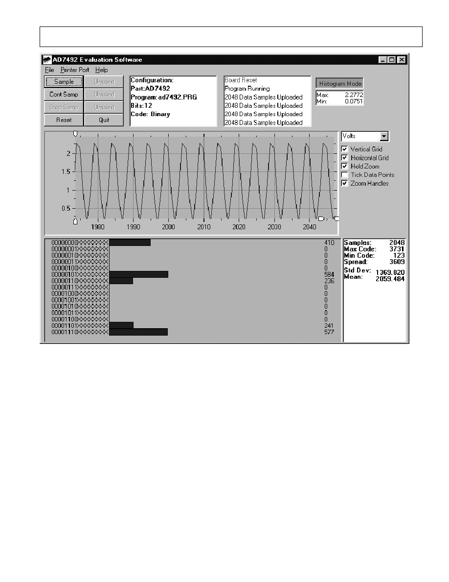
Figure 2. Main Screen
SOFTWARE DESCRIPTION
The software which controls the Evaluation Board Controller
and hence the evaluation board has three main screens.
The screen shown in Figure 2 shows the screen which appears
when the software is run. The main function of this screen is
to allow the user to read a predetermined number of samples
from the evaluation board and display them in both the time
and frequency domain. The screen can be divided into 3
sections. The upper third of the screen contains the control
buttons, the menu bar and various status windows. The
control buttons allow the user to enter the setup menu, take
samples and get information about the software. The menu
bar allows the user to select which printer port is to be used
to control the Evaluation Board Controller, load and save
data etc. The status windows indicate the setup of the
evaluation board/device, number of samples taken and any
information/error messages that are generated.
The middle third of the screen is a Digital Storage Oscilloscope
(DSO). When samples are uploaded from the Evaluation
Board Controller they are displayed here. The samples can be
displayed either as integer values or as voltages (determined
by the input range of the device inquestion). Once samples
have been displayed clicking at any point in the graph will
display the sample number and value of the point directly
beneath the cursor. Along the axis of the graph are the "zoom
handles". These allow the user to zoom in and out to get a
closer look at a particular sample if required. When another
set of samples is taken the graph will attempt to display all
values collected unless the Hold Zoom check box is ticked.
In this case the graph will keep the same axis settings as for
the previous set of data samples. Additional check boxes are
provided to give the user control over the vertical and
horizontal grids and data points. The lower third of the screen
will show either a Fast Fourier Transform (FFT) of the data
or a Histogram which shows the number of occurrances of
each particular code read back. The FFT (the default option)
is typically used when the user is concerned with examining
an ADC's performance in the frequency domain while the
Histogram will give an indication of the ADC's performance
to DC signals. The option displayed can be toggled by
clicking on the FFT Mode/Histogram Mode button in the
top right of the screen. Figure 3 shows how the main screen
looks when the Histogram Option is selected.
EVAL-AD7492CB
REV. A
7
Figure 3. Main Screen - Histogram Mode
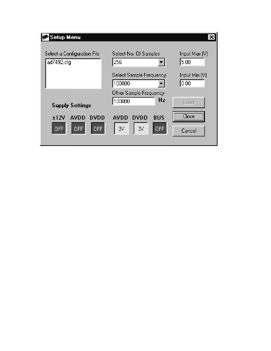
Setup Screen
The Setup Screen is responsible for allowing the user to load
a configuration file for the evaluation board. The configura-
tion file will give the software detailed information about the
evaluation board and part connected to the Evaluation Board
Controller such as number of bits, maximum sampling rate,
power supply requirements etc. The configuration file also
tells the software the name of the DSP program file which it
should download to the Evaluation Board Controller. These
files are supplied by Analog Devices with the evaluation
board. Figure 4 shows the Setup Screen.
SETTING UP THE EVALUATION BOARD CON-
TROLLER
The following text describes how the evaluation board
Evaluation Board Controller and software should be set up
for the user to begin using the complete system. The
Evaluation Board Controller and evaluation board should be
connected together (via the 96 way connector). The power
should be applied to the Evaluation Board Controller. At this
stage the red LED should be flashing which indicates that the
Evaluation Board Controller is functional and ready to
receive instructions. The software which should have
been installed should be loaded before the printer port
cable is connected between the Evaluation Board Con-troller
and the PC. This will ensure that the printer port has been
initialized properly. The printer port cable can then be
connected between the PC and the Evaluation Board Con-
troller.
Running the Software
With the hardware setup the user is now in a position to
use the software to control the Evaluation Board Con-troller
and evaluation board. In the software the user should select
the File menu and click on Setup. This will display the setup
form. A window on the left of the setup form list all the
available configuration files. The con-figuration files are text
based files which contain infor-mation about the particular
evaluation board to be tested. The information will cover
such things as the part name, number of samples to be taken,
default and maximum sampling frequency power supply
settings etc. The configuration file also contains the name of
the DSP program file which is to be downloaded to the
Evaluation Board Controller. The user should select the
relevant configuration file and click Load. The Evaluation
Board Controller will be reset and the DSP program will be
downloaded. When the download has been completed the
EVAL-AD7492CB
8
REV. A
Figure 4. Setup Screen
power supply settings indicated in the configuration file are
set and the user may hear some of the relays clicking. The
pull-down menus items such as number of samples and
sampling frequency will have been set to the default values
specified by the configuration file. The user is free to change
these at will. Once all the settings had been decided the user
can click Close to return to the main form.
Taking Samples
When the user clicks Sample the software will instruct the
Evaluation Board Controller to take the required number of
samples at the required frequency from the evaluation board.
These samples are then uploaded and displayed. An FFT and
Histogram are also calculated and displayed. If the user clicks
Cont Samp the software will repeat the process indefinitely
until the user clicks the button again. While the software is
continuously sampling data the other control buttons are
disabled.
Other Buttons
The Reset button will cause the Evaluation Board Controller
to perform a reset function. When this happens the power
supplies are turned off and the program in DSP memory is
lost. The user should repeat the setup instructions to down-
load another program if required.
The Quit button will exit the software, the program running
on the Evaluation Board Controller is not terminated.
MENU BAR ITEMS
The main screen of the Evaluation Board Controller contains
a number of options available as pull-down menu items. The
functions of these are listed below.
File Menu:
Setup Menu: Selecting this option displays the Setup Screen
as shown in Figure 4.
Load Raw Data: Selecting this option allows the user to load
data which had been saved by the software during a previous
session.
Save Raw Data: Selecting this option allows the user to save
the current set of sample data points. The data can be
reloaded to the Evaluation Board Controller software at a
later date or can be used by other programs for further
analysis
Save Binary Data: Selecting this option allows the user to
save the current set of sample data points. The data is saved
in binary format as a text file. This method can be useful for
examining code flicker, looking for stuck bits etc.
Save FFT Data: Selecting this option allows the user to save
the current set of FFT data points. FFT data cannot be
reloaded into the Evaluation Board Controller software but
can be loaded into other software packages for further
analysis.
Exit: Quits the program.
Printer Port:
This menu item allows the user to select which printer port
should be used for communication with the Evaluation Board
Controller.
LPT1: This option selects 0x378 as the printer port
address. This is the default option.
LPT2: This option selects 0x278 as the printer port
address.
PRN: This option selects 0x3BC as the printer port
address.
Help:
This menu item gives information about the current revision
of software for the particular evaluation board being used.

EVAL-AD7492CB
REV. A
9
Figure 7. AD7492 Evaluation Board Circuit Diagram (ADC Section)
SOFTWARE CONFIGURATION FILES
Software Configuration Files give the Evaluation Board Controller software information on how the software and
hardware should perform . They contain information such as the name of the DSP program to download, the default and
maximum sample frequencies, the number of samples to take and the power supply settings to use. A typical Software
Configuration File (*.cfg) is shown in Table V.
Table V.: Typical Software Configuration File.
[EVAL-CONTROL BOARD]
partname:AD7492
programname:ad7492.PRG
samplefrequency:100000
maxsamplefrequency:750000
samples:2048
+/-15V:on
dvdd:5:on
avdd:5:on
bus:on
;options 2scomp, binary
dataformat:binary
numberofbits:12
inputVmax:2.5
inputVmin:0
[endofconfig]
EVAL-AD7492CB
1 0
REV. A
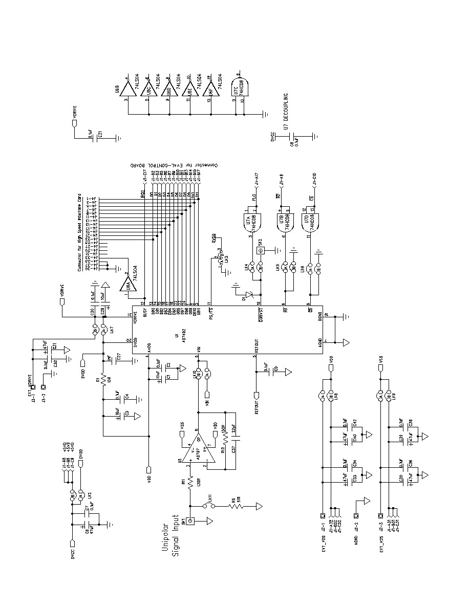
Figure 5. AD7492 Evaluation Board Circuit Diagram
EVAL-AD7492CB
REV. A
1 1
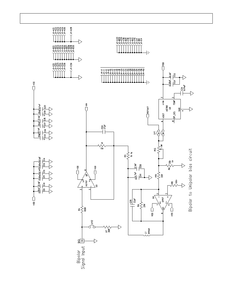
Figure 6. AD7492 Evaluation Board Circuit Diagram

EVAL-AD7492CB
1 2
REV. A
Table VI. AD7492 Evaluation Board Bill Of Materials
Qty.
PartType
RefDes
Order Number
Supplier/Manuf
1
AD7492BRU
U1
AD7492BRU
ADI
2
AD797BN
U2 U3
AD797BN
ADI
1
OP07DP
U4
OP07DP
ADI
1
AD780AR
U5
AD780AR
ADI
1
MM74HC04M
U6
.EC 379-220
Motorola
1
MM74HC08M
U7
.EC 379-224
Motorola
1
SD103C Schottky Diode
D1
SD103C
10
10u., 10V (TAJ-B Series)
C1 C3 C9 C11 C13 C15 C17
.EC 498-660
AVX
C19 C23 C29
2
0.1u. 16V X7R (0603 size)
C2 C4
.EC 499-675
AVX
13
0.1u. 50V X7R (0805 size)
C5 C7 C8 C10 C12 C14 C16
.EC 499-687
AVX
C18 C20-C22 C42 C38
5
0.1u. 50V X7R (0805 size)
C28 C30 C32 C34 C36
.EC 499-687
AVX
1
0.01u. 50V X7R (0805 size)
C24
.EC 499-225
AVX
1
27p. 50V NPO (0603 size)
C25
.EC 722-017
Philips
1
1n. 50V NPO (0805 size)
C27
.EC 317-457
AVX
6
47u. 16V (TAJ-D Series)
C6 C31 C33 C35 C40 C39
.EC 498-762
AVX
2
22p. 100V NPO (0805 size)
C37 C26
.EC-317-500
AVX
1
4.7u. 16V (TAJ-B Series)
C41
.EC 498-725
AVX
1
10
±1% (0603 Size)
R1
.EC 910-995
Multicomp
2
1K
±1% (0805 Size)
R2 R3
.EC 911-239
Multicomp
2
100
±1% (0805 Size)
R4 R8
.EC 911-732
Multicomp
2
51
±1% (0805 Size)
R5 R7
.EC 771-181
Multicomp
3
20k
±1% (0805 Size)
R6 R9 R10
.EC 771-491
Multicomp
1
130
±1% (0805 Size)
R11
.EC 771-235
Multicomp
1
130
±1% (0805 Size)
R12
.EC 771-235
Multicomp
1
50K
Multi-turn trimmer pot
R13
.EC 348-144
Bourns
1
220uH Inductor (8RHB Series)
L1
.EC 598-215
TOKO
1
2 pin header
LK1
.EC 511-705
Harwin
8
4 (2+2) pin header
LK2 LK4 LK5 LK6 LK7 LK8 LK9 LK10
.EC 511-791
Harwin
1
3 pin header (SIP3)
LK3
.EC 671-927
Harwin
10
Shorting Link
LK1 - LK10
.EC 528-456
Berg
24
Ultra Low Profile Sockets
U3 U4 U5
.EC 519-959
Harwin
1
96 Pin 90º DIN41612 Plug
J1
.EC 269-931
Siemens
1
3 Pin Terminal Block
J2
.EC 151-786
Lumberg
1
2 Pin Terminal Block
J3
.EC 151-785
Lumberg
1
40 Pin 90º IDC Ribbon Connector
J4
.EC 727-714
3M
3
Gold 50
SMB Jack
SK1 SK2 SK3
.EC 310-682
M/ACOM
4
Stick-on .eet
Each Corner
.EC 148-922
3M
1
PCB
EVAL-AD7492CB
n/a
EVAL-AD7492CB
REV. A
1 3
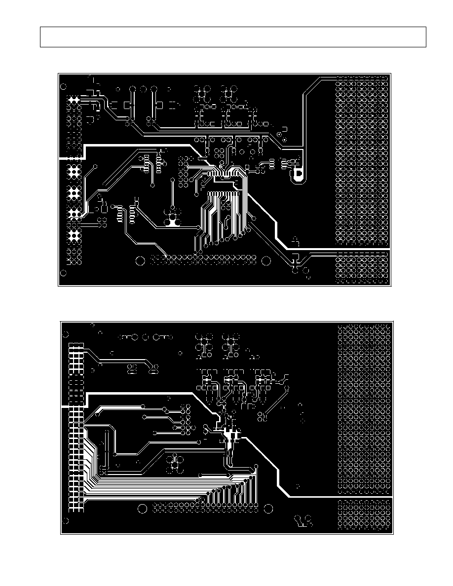
Figure 7. Component Side Artwork
Figure 8. Solder Side Artwork
EVAL-AD7492CB
1 4
REV. A
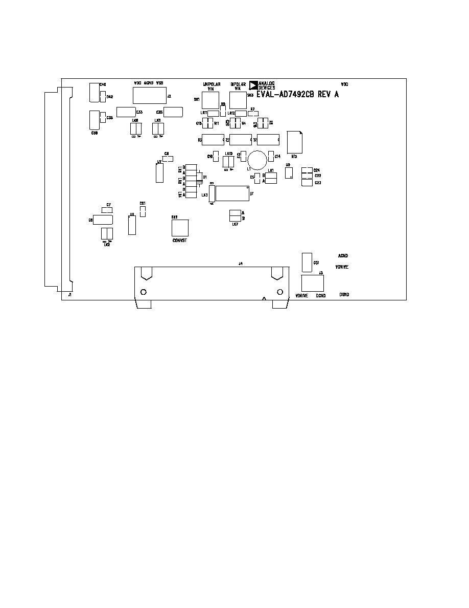
Figure 6. Component Side Artwork