Äîêóìåíòàöèÿ è îïèñàíèÿ www.docs.chipfind.ru
REV. A
Information furnished by Analog Devices is believed to be accurate and
reliable. However, no responsibility is assumed by Analog Devices for its
use, nor for any infringements of patents or other rights of third parties
which may result from its use. No license is granted by implication or
otherwise under any patent or patent rights of Analog Devices.
a
AD73360
One Technology Way, P.O. Box 9106, Norwood, MA 02062-9106, U.S.A.
Tel: 781/329-4700
World Wide Web Site: http://www.analog.com
Fax: 781/326-8703
© Analog Devices, Inc., 2000
Six-Input Channel
Analog Front End
FEATURES
Six 16-Bit A/D Converters
Programmable Input Sample Rate
Simultaneous Sampling
77 dB SNR
64 kS/s Maximum Sample Rate
83 dB Crosstalk
Low Group Delay (25
s Typ per ADC Channel)
Programmable Input Gain
Flexible Serial Port which Allows Multiple Devices to
Be Connected in Cascade
Single (+2.7 V to +5.5 V) Supply Operation
80 mW Max Power Consumption at +2.7 V
On-Chip Reference
28-Lead SOIC and 44-Lead TQFP Packages
APPLICATIONS
General Purpose Analog Input
Industrial Power Metering
Motor Control
Simultaneous Sampling Applications
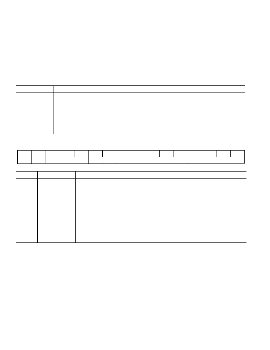
FUNCTIONAL BLOCK DIAGRAM
VINN1
VINP1
ANALOG
-
MODULATOR
SDI
SDIFS
SCLK
REFCAP
REFOUT
SE
RESET
SDOFS
SDO
MCLK
VINN2
VINP2
VINN3
VINP3
VINN4
VINP4
VINN5
VINP5
VINN6
VINP6
AD73360
SIGNAL
CONDITIONING
0/38dB
PGA
DECIMATOR
SERIAL
I/O
PORT
ANALOG
-
MODULATOR
SIGNAL
CONDITIONING
0/38dB
PGA
DECIMATOR
ANALOG
-
MODULATOR
SIGNAL
CONDITIONING
0/38dB
PGA
DECIMATOR
ANALOG
-
MODULATOR
SIGNAL
CONDITIONING
0/38dB
PGA
DECIMATOR
ANALOG
-
MODULATOR
SIGNAL
CONDITIONING
0/38dB
PGA
DECIMATOR
ANALOG
-
MODULATOR
SIGNAL
CONDITIONING
0/38dB
PGA
DECIMATOR
REFERENCE
GENERAL DESCRIPTION
The AD73360 is a six-input channel analog front-end processor
for general purpose applications including industrial power
metering or multichannel analog inputs. It features six 16-bit
A/D conversion channels each of which provide 77 dB signal-to-
noise ratio over a dc to 4 kHz signal bandwidth. Each channel
also features a programmable input gain amplifier (PGA) with
gain settings in eight stages from 0 dB to 38 dB.
The AD73360 is particularly suitable for industrial power me-
tering as each channel samples synchronously, ensuring that there
is no (phase) delay between the conversions. The AD73360 also
features low group delay conversions on all channels.
An on-chip reference voltage is included and is programmable
to accommodate either 3 V or 5 V operation.
The sampling rate of the device is programmable with four
separate settings offering 64 kHz, 32 kHz, 16 kHz and 8 kHz
sampling rates (from a master clock of 16.384 MHz).
A serial port (SPORT) allows easy interfacing of single or cas-
caded devices to industry standard DSP engines. The SPORT
transfer rate is programmable to allow interfacing to both fast
and slow DSP engines.
The AD73360 is available in 28-lead SOIC and 44-lead TQFP
packages.

REV. A
2
AD73360SPECIFICATIONS
1
(AVDD = 3 V 10%; DVDD = 3 V 10%; DGND = AGND = 0 V, f
MCLK
= 16.384 MHz,
f
SCLK
= 8.192 MHz, f
S
= 8 kHz; T
A
= T
MIN
to T
MAX
, unless otherwise noted.)
AD73360A
Parameter
Min
Typ
Max
Unit
Test Conditions/Comments
REFERENCE
REFCAP
Absolute Voltage, V
REFCAP
1.125
1.25
1.375
V
5VEN = 0
REFCAP TC
50
ppm/
°C
0.1
µF Capacitor Required from REFCAP
to AGND2
REFOUT
Typical Output Impedance
130
Absolute Voltage, V
REFOUT
1.125
1.25
1.375
V
Unloaded
Minimum Load Resistance
1
k
Maximum Load Capacitance
100
pF
ADC SPECIFICATIONS
Maximum Input Range at VIN
2, 3
1.644
V p-p
5VEN = 0, Measured Differentially
2.85
dBm
Nominal Reference Level at VIN
1.1413
V p-p
5VEN = 0, Measured Differentially
(0 dBm0)
6.02
dBm
Absolute Gain
PGA = 0 dB
0.8
+0.8
dB
1.0 kHz
PGA = 38 dB
0.8
+0.8
dB
1.0 kHz
Gain Tracking Error
±0.1
dB
1.0 kHz, +3 dBm0 to 50 dBm0
Signal to (Noise + Distortion)
PGA = 0 dB
73
77
dB
0 Hz to 4 kHz; f
S
= 8 kHz
PGA = 38 dB
62
dB
0 Hz to 4 kHz; f
S
= 64 kHz
Total Harmonic Distortion
PGA = 0 dB
83
76
dB
PGA = 38 dB
70
dB
Intermodulation Distortion
76
dB
PGA = 0 dB
Idle Channel Noise
70
dB
PGA = 0 dB
Crosstalk ADC-to-ADC
83
dB
ADC1 Input Signal Level: 1.0 kHz
ADC2 Input at Idle
DC Offset
30
+10
+45
mV
PGA = 0 dB
Power Supply Rejection
55
dB
Input Signal Level at AVDD and DVDD
Pins 1.0 kHz, 100 mV p-p Sine Wave
Group Delay
4, 5
25
µs
64 kHz Output Sample Rate
50
µs
32 kHz Output Sample Rate
95
µs
16 kHz Output Sample Rate
190
µs
8 kHz Output Sample Rate
Input Resistance at VIN
2, 4
25
k
6
DMCLK = 16.384 MHz
FREQUENCY RESPONSE
(ADC)
7
Typical Output
Frequency (Normalized to f
S
)
0
0
dB
0.03125
0.1
dB
0.0625
0.25
dB
0.125
0.6
dB
0.1875
1.4
dB
0.25
2.8
dB
0.3125
4.5
dB
0.375
7.0
dB
0.4375
9.5
dB
> 0.5
< 12.5
dB
REV. A
3
AD73360
AD73360A
Parameter
Min
Typ
Max
Unit
Test Conditions/Comments
LOGIC INPUTS
V
INH
, Input High Voltage
V
DD
0.8
V
DD
V
V
INL
, Input Low Voltage
0
0.8
V
I
IH
, Input Current
10
µA
C
IN
, Input Capacitance
10
pF
LOGIC OUTPUTS
V
OH
, Output High Voltage
V
DD
0.4
V
DD
V
|IOUT|
100 µA
V
OL
, Output Low Voltage
0
0.4
V
|IOUT|
100 µA
Three-State Leakage Current
10
+10
µA
POWER SUPPLIES
AVDD1, AVDD2
2.7
3.3
V
DVDD
2.7
3.3
V
I
DD
8
See Table I
NOTES
1
Operating temperature range is as follows: 40
°C to +85°C. Therefore, T
MIN
= 40
°C and T
MAX
= +85
°C.
2
Test conditions: Input PGA set for 0 dB gain (unless otherwise noted).
3
At input to sigma-delta modulator of ADC.
4
Guaranteed by design.
5
Overall group delay will be affected by the sample rate and the external digital filtering.
6
The ADC's input impedance is inversely proportional to DMCLK and is approximated by: (4
× 10
11
)/DMCLK.
7
Frequency response of ADC measured with input at audio reference level (the input level that produces an output level of 10 dBm0), with 38 dB preamplifier
bypassed and input gain of 0 dB.
8
Test Conditions: no load on digital inputs, analog inputs ac coupled to ground.
Specifications subject to change without notice.
Table I. Current Summary (AVDD = DVDD = 3.3 V)
Total
Analog
Digital
Current
MCLK
Conditions
Current
Current
(Max)
SE
ON
Comments
ADCs Only On
12
10
26.5
1
YES
REFOUT Disabled
REFCAP Only On
0.75
0.04
1.0
0
NO
REFOUT Disabled
REFCAP and
REFOUT Only On
3.3
0.04
4.5
0
NO
All Sections Off
0.01
1.2
1.5
0
YES
MCLK Active Levels Equal to 0 V and DVDD
All Sections Off
0.01
0.03
0.1
0
NO
Digital Inputs Static and Equal to 0 V or DVDD
The above values are in mA and are typical values unless otherwise noted. MCLK = 16.384 MHz; SCLK = 16.384 MHz.

REV. A
4
AD73360SPECIFICATIONS
1
(AVDD = 5 V 10%; DVDD = 5 V 10%; DGND = AGND = 0 V, f
MCLK
= 16.384 MHz,
f
SCLK
= 8.192 MHz, f
S
= 8 kHz; T
A
= T
MIN
to T
MAX
, unless otherwise noted.)
AD73360A
Parameter
Min
Typ
Max
Unit
Test Conditions/Comments
REFERENCE
REFCAP
Absolute Voltage, V
REFCAP
1.25
V
5VEN = 0
2.5
V
5VEN = 1
REFCAP TC
50
ppm/
°C
0.1
µF Capacitor Required from REFCAP
to AGND2
REFOUT
Typical Output Impedance
130
Absolute Voltage, V
REFOUT
1.25
V
5VEN = 0, Unloaded
2.5
V
5VEN = 1, Unloaded
Minimum Load Resistance
2
k
5VEN = 1
Maximum Load Capacitance
100
pF
ADC SPECIFICATIONS
Maximum Input Range at VIN
2, 3
3.2875
V p-p
5VEN = 1, Measured Differentially
3.17
dBm
Nominal Reference Level at VIN
2.2823
V p-p
5VEN = 1, Measured Differentially
(0 dBm0)
0
dBm
Absolute Gain
PGA = 0 dB
0.1
dB
1.0 kHz
PGA = 38 dB
0.5
dB
1.0 kHz
Gain Tracking Error
±0.1
dB
1.0 kHz, +3 dBm0 to 50 dBm0
Signal to (Noise + Distortion)
PGA = 0 dB
76
dB
0 Hz to 4 kHz; f
S
= 8 kHz
PGA = 38 dB
70
dB
0 Hz to 4 kHz; f
S
= 64 kHz
Total Harmonic Distortion
PGA = 0 dB
86
dB
PGA = 38 dB
80
dB
Intermodulation Distortion
79
dB
PGA = 0 dB
Idle Channel Noise
76
dB
PGA = 0 dB
Crosstalk ADC-to-ADC
85
dB
ADC1 Input Signal Level: 1.0 kHz, 0 dBm0
ADC2 Input at Idle
DC Offset
20
mV
PGA = 0 dB
Power Supply Rejection
55
dB
Input Signal Level at AVDD and DVDD
Pins 1.0 kHz, 100 mV p-p Sine Wave
Group Delay
4, 5
25
µs
64 kHz Output Sample Rate
50
µs
32 kHz Output Sample Rate
95
µs
16 kHz Output Sample Rate
190
µs
8 kHz Output Sample Rate
Input Resistance at VIN
2, 4
25
k
6
DMCLK = 16.384 MHz
FREQUENCY RESPONSE
(ADC)
7
Typical Output
Frequency (Normalized to f
S
)
0
0
dB
0.03125
0.1
dB
0.0625
0.25
dB
0.125
0.6
dB
0.1875
1.4
dB
0.25
2.8
dB
0.3125
4.5
dB
0.375
7.0
dB
0.4375
9.5
dB
> 0.5
< 12.5
dB
REV. A
5
AD73360
AD73360A
Parameter
Min
Typ
Max
Unit
Test Conditions/Comments
LOGIC INPUTS
V
INH
, Input High Voltage
V
DD
0.8
V
DD
V
V
INL
, Input Low Voltage
0
0.8
V
I
IH
, Input Current
0.5
µA
C
IN
, Input Capacitance
10
pF
LOGIC OUTPUTS
V
OH
, Output High Voltage
V
DD
0.4
V
DD
V
|IOUT|
100 µA
V
OL
, Output Low Voltage
0
0.4
V
|IOUT|
100 µA
Three-State Leakage Current
0.3
µA
POWER SUPPLIES
AVDD1, AVDD2
4.5
5.5
V
DVDD
4.5
5.5
V
I
DD
8
See Table II
NOTES
1
Operating temperature range is as follows: 40
°C to +85°C. Therefore, T
MIN
= 40
°C and T
MAX
= +85
°C.
2
Test conditions: Input PGA set for 0 dB gain (unless otherwise noted).
3
At input to sigma-delta modulator of ADC.
4
Guaranteed by design.
5
Overall group delay will be affected by the sample rate and the external digital filtering.
6
The ADC's input impedance is inversely proportional to DMCLK and is approximated by: (4
× 10
11
)/DMCLK.
7
Frequency response of ADC measured with input at audio reference level (the input level that produces an output level of 10 dBm0), with 38 dB preamplifier
bypassed and input gain of 0 dB.
8
Test Conditions: no load on digital inputs, analog inputs ac coupled to ground.
Specifications subject to change without notice.
Table II. Current Summary (AVDD = DVDD = 5.5 V)
Total
Analog
Digital
Current
MCLK
Conditions
Current
Current
(Typ)
SE
ON
Comments
ADCs Only On
16
16
32
1
YES
REFOUT Disabled
REFCAP Only On
0.8
0
0.8
0
NO
REFOUT Disabled
REFCAP and
REFOUT Only On
3.5
0
3.5
0
NO
All Sections Off
0.1
1.9
2.0
0
YES
MCLK Active Levels Equal to 0 V and DVDD
All Sections Off
0
0.05
0.06
0
NO
Digital Inputs Static and Equal to 0 V or DVDD
The above values are in mA and are typical values unless otherwise noted.
Table III. Signal Ranges
3 V Power Supply
5 V Power Supply
5VEN = 0
5VEN = 0
5VEN = 1
V
REFCAP
1.25 V
± 10%
1.25 V
2.5 V
V
REFOUT
1.25 V
± 10%
1.25 V
2.5 V
ADC
Maximum Input Range at V
IN
1.64375 V p-p
1.64375 V p-p
3.2875 V p-p
Nominal Reference Level
1.1413 V p-p
1.1413 V p-p
2.2823 V p-p

REV. A
AD73360
6
TIMING CHARACTERISTICS
Limit at
Parameter
T
A
= 40 C to +85 C
Unit
Description
Clock Signals
See Figure 1
t
1
61
ns min
MCLK Period
t
2
24.4
ns min
MCLK Width High
t
3
24.4
ns min
MCLK Width Low
Serial Port
See Figures 3 and 4
t
4
t
1
ns min
SCLK Period
t
5
0.4
× t
1
ns min
SCLK Width High
t
6
0.4
× t
1
ns min
SCLK Width Low
t
7
20
ns min
SDI/SDIFS Setup Before SCLK Low
t
8
0
ns min
SDI/SDIFS Hold After SCLK Low
t
9
10
ns max
SDOFS Delay from SCLK High
t
10
10
ns min
SDOFS Hold After SCLK High
t
11
10
ns min
SDO Hold After SCLK High
t
12
10
ns max
SDO Delay from SCLK High
t
13
30
ns max
SCLK Delay from MCLK
(AVDD = 3 V 10%; DVDD = 3 V 10%; AGND = DGND = 0 V; T
A
= T
MlN
to T
MAX
, unless otherwise
noted)
TIMING CHARACTERISTICS
Limit at
Parameter
T
A
= 40 C to +85 C
Unit
Description
Clock Signals
See Figure 1
t
1
61
ns min
MCLK Period
t
2
24.4
ns min
MCLK Width High
t
3
24.4
ns min
MCLK Width Low
Serial Port
See Figures 3 and 4
t
4
t
1
ns min
SCLK Period
t
5
0.4
× t
1
ns min
SCLK Width High
t
6
0.4
× t
1
ns min
SCLK Width Low
t
7
20
ns min
SDI/SDIFS Setup Before SCLK Low
t
8
0
ns min
SDI/SDIFS Hold After SCLK Low
t
9
10
ns max
SDOFS Delay from SCLK High
t
10
10
ns min
SDOFS Hold After SCLK High
t
11
10
ns min
SDO Hold After SCLK High
t
12
10
ns max
SDO Delay from SCLK High
t
13
30
ns max
SCLK Delay from MCLK
(AVDD = 5 V 10%; DVDD = 5 V 10%; AGND = DGND = 0 V; T
A
= T
MlN
to T
MAX
, unless otherwise
noted)
REV. A
AD73360
7
t
3
t
2
t
1
Figure 1. MCLK Timing
TO OUTPUT
PIN
+2.1V
100 A
100 A
I
OL
I
OH
C
L
15pF
Figure 2. Load Circuit for Timing Specifications
t
3
t
1
t
2
t
13
* SCLK IS INDIVIDUALLY PROGRAMMABLE
IN FREQUENCY (MCLK/4 SHOWN HERE).
t
4
t
5
t
6
MCLK
SCLK*
Figure 3. SCLK Timing
t
11
t
7
t
9
t
10
t
12
t
7
t
8
SE (I)
SCLK (O)
SDIFS (I)
SDI (I)
SDOFS (O)
SDO (O)
THREE-
STATE
THREE-
STATE
THREE-
STATE
D15
D2
D1
D0
D14
D15
D1
D14
D15
D15
t
8
D0
Figure 4. Serial Port (SPORT)
V
IN
dBm0
85
5
75
65
55
45
35
25
15
5
80
70
10
S/(N+D) dB
30
20
10
0
50
40
60
3.17
Figure 5a. S/(N+D) vs. V
IN
(ADC @ 3 V) Over Voiceband
Bandwidth (300 Hz3.4 kHz)
V
IN
dBm0
85
5
75
65
55
45
35
25
15
5
80
70
10
S/(N+D)
dB
30
20
10
0
50
40
60
3.17
Figure 5b. S/(N+D) vs. V
IN
(ADC @ 5 V) Over Voiceband
Bandwidth (300 Hz3.4 kHz)
REV. A
AD73360
8
ABSOLUTE MAXIMUM RATINGS*
(T
A
= +25
°C unless otherwise noted)
AVDD, DVDD to GND . . . . . . . . . . . . . . . . . 0.3 V to +7 V
AGND to DGND . . . . . . . . . . . . . . . . . . . . . 0.3 V to +0.3 V
Digital I/O Voltage to DGND . . . . . . 0.3 V to DVDD + 0.3 V
Analog I/O Voltage to AGND . . . . . 0.3 V to AVDD + 0.3 V
Operating Temperature Range
Industrial (A Version) . . . . . . . . . . . . . . . . 40
°C to +85°C
Storage Temperature Range . . . . . . . . . . . . 65
°C to +150°C
Maximum Junction Temperature . . . . . . . . . . . . . . . . +150
°C
SOIC,
JA
Thermal Impedance . . . . . . . . . . . . . . . . . . 75
°C/W
Lead Temperature, Soldering
Vapor Phase (60 sec) . . . . . . . . . . . . . . . . . . . . . . . . +215
°C
Infrared (15 sec) . . . . . . . . . . . . . . . . . . . . . . . . . . . . +220
°C
*Stresses above those listed under Absolute Maximum Ratings may cause perma-
nent damage to the device. This is a stress rating only; functional operation of the
device at these or any other conditions above those listed in the operational sections
of this specification is not implied. Exposure to absolute maximum rating condi-
tions for extended periods may affect device reliability.
ORDERING GUIDE
Temperature
Package
Model
Range
Options
1
AD73360AR
40
°C to +85°C
R-28
AD73360ASU
40
°C to +85°C
SU-44
EVAL-AD73360EB
Evaluation Board
2
+EZ-KIT Lite Upgrade
3
EVAL-AD73360EZ
Evaluation Board
2
+EZ-KIT Lite
4
NOTES
1
R = 0.3' Small Outline IC (SOIC); SU = Thin Quad Flatpack IC (TQFP).
2
The AD73360 evaluation board can be interfaced to an ADSP-2181 EZ-KIT Lite
or to a Texas Instruments EVM kit.
3
The upgrade consists of a connector for the expansion port P3 of the EZ-KIT
Lite. This option is intended for existing owners of EZ-KIT Lite.
4
The EZ-KIT Lite has been modified to allow it to interface with the AD73360
evaluation board. This option is intended for users who do not already have an
EZ-KIT Lite.
CAUTION
ESD (electrostatic discharge) sensitive device. Electrostatic charges as high as 4000 V readily
accumulate on the human body and test equipment and can discharge without detection.
Although the AD73360 features proprietary ESD protection circuitry, permanent damage may
occur on devices subjected to high energy electrostatic discharges. Therefore, proper ESD
precautions are recommended to avoid performance degradation or loss of functionality.
WARNING!
ESD SENSITIVE DEVICE
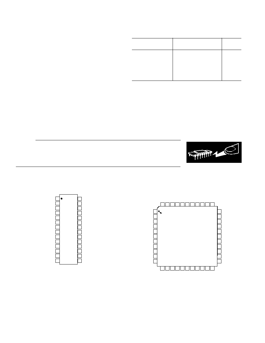
PIN CONFIGURATIONS
R-28
SU-44
TOP VIEW
(Not to Scale)
28
27
26
25
24
23
22
21
20
19
18
17
16
15
1
2
3
4
5
6
7
8
9
10
11
12
13
14
AD73360
SDO
MCLK
SCLK
RESET
DVDD
DGND
AGND2
VINP2
VINN2
VINP1
VINN1
AVDD2
REFCAP
REFOUT
SDOFS
SDIFS
SDI
SE
AGND1
AVDD1
VINP6
VINN3
VINP3
VINN4
VINP4
VINN6
VINP5
VINN5
3
4
5
6
7
1
2
10
11
8
9
40 39 38
41
42
43
44
36 35 34
37
12 13
14 15 16 17 18 19 20 21 22
PIN 1
IDENTIFIER
TOP VIEW
(Not to Scale)
29
30
31
32
33
27
28
25
26
23
24
NC
VINN5
VINP5
NC
VINN6
VINP6
NC
REFOUT
REFCAP
AVDD2
AVDD2
AGND2
AGND2
AGND2
NC = NO CONNECT
AGND2
DGND
DGND
DVDD
AVDD1
SDI
NC
AVDD1
SDIFS
AGND1
AGND1
NC
VINN1
NC
RESETB
VINN2
VINP3
VINN4
VINP4
NC
VINP2
SCLK
MCLK
SDO
VINP1
NC
SDOFS
VINN3
SE
NC
AD73360

REV. A
AD73360
9
PIN FUNCTION DESCRIPTION
Mnemonic
Function
VINP1
Analog Input to the Positive Terminal of Input Channel 1.
VINN1
Analog Input to the Negative Terminal of Input Channel 1.
VINP2
Analog Input to the Positive Terminal of Input Channel 2.
VINN2
Analog Input to the Negative Terminal of Input Channel 2.
VINP3
Analog Input to the Positive Terminal of Input Channel 3.
VINN3
Analog Input to the Negative Terminal of Input Channel 3.
VINP4
Analog Input to the Positive Terminal of Input Channel 4.
VINN4
Analog Input to the Negative Terminal of Input Channel 4.
VINP5
Analog Input to the Positive Terminal of Input Channel 5.
VINN5
Analog Input to the Negative Terminal of Input Channel 5.
VINP6
Analog Input to the Positive Terminal of Input Channel 6.
VINN6
Analog Input to the Negative Terminal of Input Channel 6.
REFOUT
Buffered Reference Output, which has a nominal value of 1.25 V or 2.5 V, the value being dependent on the status
of Bit 5VEN (CRC:7).
REFCAP
A Bypass Capacitor to AGND2 of 0.1
µF is required for the on-chip reference. The capacitor should be fixed to
this pin. This pin can be overdriven by an external reference if required.
AVDD2
Analog Power Supply Connection.
AGND2
Analog Ground/Substrate Connection.
DGND
Digital Ground/Substrate Connection.
DVDD
Digital Power Supply Connection.
RESET
Active Low Reset Signal. This input resets the entire chip, resetting the control registers and clearing the digital
circuitry.
SCLK
Output Serial Clock whose rate determines the serial transfer rate to/from the AD73360. It is used to clock data or
control information to and from the serial port (SPORT). The frequency of SCLK is equal to the frequency of the
master clock (MCLK) divided by an integer number--this integer number being the product of the external mas-
ter clock rate divider and the serial clock rate divider.
MCLK
Master Clock Input. MCLK is driven from an external clock signal.
SDO
Serial Data Output of the AD73360. Both data and control information may be output on this pin and are clocked
on the positive edge of SCLK. SDO is in three-state when no information is being transmitted and when SE is
low.
SDOFS
Framing Signal Output for SDO Serial Transfers. The frame sync is one bit wide and it is active one SCLK period
before the first bit (MSB) of each output word. SDOFS is referenced to the positive edge of SCLK. SDOFS is in
three-state when SE is low.
SDIFS
Framing Signal Input for SDI Serial Transfers. The frame sync is one bit wide and it is valid one SCLK period
before the first bit (MSB) of each input word. SDIFS is sampled on the negative edge of SCLK and is ignored
when SE is low.
SDI
Serial Data Input of the AD73360. Both data and control information may be input on this pin and are clocked on
the negative edge of SCLK. SDI is ignored when SE is low.
SE
SPORT Enable. Asynchronous input enable pin for the SPORT. When SE is set low by the DSP, the output pins
of the SPORT are three-stated and the input pins are ignored. SCLK is also disabled internally in order to decrease
power dissipation. When SE is brought high, the control and data registers of the SPORT are at their original values
(before SE was brought low); however, the timing counters and other internal registers are at their reset values.
AGND1
Analog Ground Connection.
AVDD1
Analog Power Supply Connection.

REV. A
AD73360
10
TERMINOLOGY
Absolute Gain
Absolute gain is a measure of converter gain for a known signal.
Absolute gain is measured (differentially) with a 1 kHz sine
wave at 0 dBm0 for each ADC. The absolute gain specification
is used for gain tracking error specification.
Crosstalk
Crosstalk is due to coupling of signals from a given channel to
an adjacent channel. It is defined as the ratio of the amplitude of
the coupled signal to the amplitude of the input signal. Crosstalk
is expressed in dB.
Gain Tracking Error
Gain tracking error measures changes in converter output for
different signal levels relative to an absolute signal level. The
absolute signal level is 0 dBm0 (equal to absolute gain) at 1 kHz
for each ADC. Gain tracking error at 0 dBm0 (ADC) is 0 dB by
definition.
Group Delay
Group Delay is defined as the derivative of radian phase with
respect to radian frequency, dø(f)/df. Group delay is a measure
of average delay of a system as a function of frequency. A linear
system with a constant group delay has a linear phase response.
The deviation of group delay from a constant indicates the de-
gree of nonlinear phase response of the system.
Idle Channel Noise
Idle channel noise is defined as the total signal energy measured
at the output of the device when the input is grounded (mea-
sured in the frequency range 0 Hz4 kHz).
Intermodulation Distortion
With inputs consisting of sine waves at two frequencies, fa and
fb, any active device with nonlinearities will create distortion
products at sum and difference frequencies of mfa
± nfb where
m, n = 0, 1, 2, 3, etc. Intermodulation terms are those for which
neither m nor n are equal to zero. For final testing, the second
order terms include (fa + fb) and (fa fb), while the third order
terms include (2fa + fb), (2fa fb), (fa + 2fb) and (fa 2fb).
Power Supply Rejection
Power supply rejection measures the susceptibility of a device to
noise on the power supply. Power supply rejection is measured
by modulating the power supply with a sine wave and measuring
the noise at the output (relative to 0 dB).
Sample Rate
The sample rate is the rate at which each ADC updates its out-
put register. It is set relative to the DMCLK and the program-
mable sample rate setting.
SNR + THD
Signal-to-noise ratio plus harmonic distortion is defined to be
the ratio of the rms value of the measured input signal to the
rms sum of all other spectral components in a given frequency
range, including harmonics but excluding dc.
ABBREVIATIONS
ADC
Analog-to-Digital Converter.
BW
Bandwidth.
CRx
A Control Register where x is a placeholder for
an alphabetic character (AE). There are eight
read/write control registers on the AD73360--
designated CRA through CRE.
CRx:n
A bit position, where n is a placeholder for a
numeric character (07), within a control regis-
ter; where x is a placeholder for an alphabetic
character (AE). Position 7 represents the MSB
and Position 0 represents the LSB.
DMCLK
Device (Internal) Master Clock. This is the
internal master clock resulting from the external
master clock (MCLK) being divided by the on-
chip master clock divider.
FSLB
Frame Sync Loop-Back--where the SDOFS of
the final device in a cascade is connected to the
RFS and TFS of the DSP and the SDIFS of first
device in the cascade. Data input and output
occur simultaneously. In the case of nonFSLB,
SDOFS and SDO are connected to the Rx Port
of the DSP while SDIFS and SDI are connected
to the Tx Port.
PGA
Programmable Gain Amplifier.
SC
Switched Capacitor.
SNR
Signal-to-Noise Ratio.
SPORT
Serial Port.
THD
Total Harmonic Distortion.
VBW
Voice Bandwidth.
REV. A
AD73360
11
FUNCTIONAL DESCRIPTION
General Description
The AD73360 is a six-channel, 16-bit, analog front end. It
comprises six independent encoder channels each featuring
signal conditioning, programmable gain amplifier, sigma-delta
A/D convertor and decimator sections. Each of these sections is
described in further detail below.
Encoder Channel
Each encoder channel consists of a signal conditioner, a
switched capacitor PGA and a sigma-delta analog-to-digital
converter (ADC). An on-board digital filter, which forms part
of the sigma-delta ADC, also performs critical system-level
filtering. Due to the high level of oversampling, the input
antialias requirements are reduced such that a simple single pole
RC stage is sufficient to give adequate attenuation in the band
of interest.
Signal Conditioner
Each analog channel has an independent signal conditioning
block. This allows the analog input to be configured by the user
depending on whether differential or single-ended mode is used.
Programmable Gain Amplifier
Each encoder section's analog front end comprises a switched
capacitor PGA that also forms part of the sigma-delta modula-
tor. The SC sampling frequency is DMCLK/8. The PGA,
whose programmable gain settings are shown in Table IV, may
be used to increase the signal level applied to the ADC from low
output sources such as microphones, and can be used to avoid
placing external amplifiers in the circuit. The input signal level
to the sigma-delta modulator should not exceed the maximum
input voltage permitted.
The PGA gain is set by bits IGS0, IGS1 and IGS2 in control
Registers D, E and F.
Table IV. PGA Settings for the Encoder Channel
IxGS2
IxGS1
IxGS0
Gain (dB)
0
0
0
0
0
0
1
6
0
1
0
12
0
1
1
18
1
0
0
20
1
0
1
26
1
1
0
32
1
1
1
38
ADC
Each channel has its own ADC consisting of an analog sigma-
delta modulator and a digital antialiasing decimation filter. The
sigma-delta modulator noise-shapes the signal and produces
1-bit samples at a DMCLK/8 rate. This bitstream, representing
the analog input signal, is input to the antialiasing decimation
filter. The decimation filter reduces the sample rate and in-
creases the resolution.
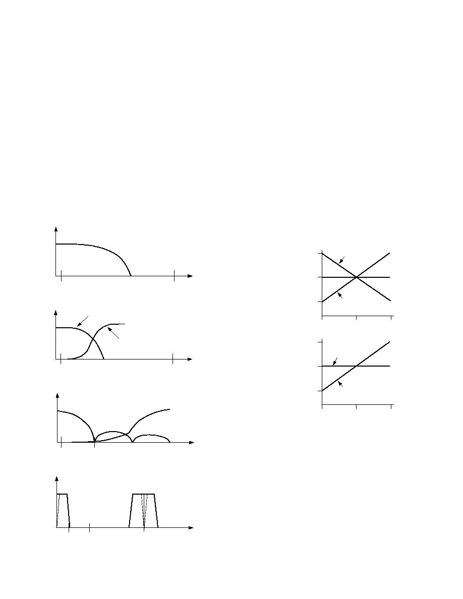
Analog Sigma-Delta Modulator
The AD73360 input channels employ a sigma-delta conversion
technique, which provides a high resolution 16-bit output with
system filtering being implemented on-chip.
Sigma-delta converters employ a technique known as over-
sampling, where the sampling rate is many times the highest
frequency of interest. In the case of the AD73360, the initial
sampling rate of the sigma-delta modulator is DMCLK/8. The
main effect of oversampling is that the quantization noise is
spread over a very wide bandwidth, up to f
S
/2 = DMCLK/16
(Figure 6a). This means that the noise in the band of interest is
much reduced. Another complementary feature of sigma-delta
converters is the use of a technique called noise-shaping. This
technique has the effect of pushing the noise from the band of
interest to an out-of-band position (Figure 6b). The combina-
tion of these techniques, followed by the application of a digital
filter, reduces the noise in band sufficiently to ensure good
dynamic performance from the part (Figure 6c).
BAND
OF
INTEREST
F
S
/2
DMCLK/16
F
S
/2
DMCLK/16
F
S
/2
DMCLK/16
DIGITAL FILTER
NOISE-SHAPING
BAND
OF
INTEREST
BAND
OF
INTEREST
a.
b.
c.
Figure 6. Sigma-Delta Noise Reduction
REV. A
AD73360
12
Figure 7 shows the various stages of filtering that are employed
in a typical AD73360 application. In Figure 7a we see the trans-
fer function of the external analog antialias filter. Even though it
is a single RC pole, its cutoff frequency is sufficiently far away
from the initial sampling frequency (DMCLK/8) that it takes
care of any signals that could be aliased by the sampling fre-
quency. This also shows the major difference between the initial
oversampling rate and the bandwidth of interest. In Figure 7b,
the signal and noise-shaping responses of the sigma-delta modu-
lator are shown. The signal response provides further rejection
of any high frequency signals while the noise-shaping will push
the inherent quantization noise to an out-of-band position. The
detail of Figure 7c shows the response of the digital decima-
tion filter (Sinc-cubed response) with nulls every multiple of
DMCLK/256, which is the decimation filter update rate. The
final detail in Figure 7d shows the application of a final antialias
filter in the DSP engine. This has the advantage of being imple-
mented according to the user's requirements and available
MIPS. The filtering in Figures 7a through 7c is implemented in
the AD73360.
F
B
= 4kHz
F
SINIT
= DMCLK/8
a. Analog Antialias Filter Transfer Function
F
B
= 4kHz
F
SINIT
= DMCLK/8
NOISE TRANSFER FUNCTION
SIGNAL TRANSFER FUNCTION
b. Analog Sigma-Delta Modulator Transfer Function
F
B
= 4kHz
F
SINTER
= DMCLK/256
c. Digital Decimator Transfer Function
F
B
= 4kHz
F
SINTER
= DMCLK/256
F
SFINAL
= 8kHz
d. Final Filter LPF (HPF) Transfer Function
Figure 7. DC Frequency Responses
Decimation Filter
The digital filter used in the AD73360 carries out two important
functions. Firstly, it removes the out-of-band quantization noise,
which is shaped by the analog modulator and secondly, it deci-
mates the high frequency bitstream to a lower rate 15-bit word.
The antialiasing decimation filter is a sinc-cubed digital filter
that reduces the sampling rate from DMCLK/8 to DMCLK/
256, and increases the resolution from a single bit to 15 bits. Its
Z transform is given as: [(1Z
32
)/(1Z
1
)]
3
. This ensures a mini-
mal group delay of 25
µs.
ADC Coding
The ADC coding scheme is in twos complement format (see
Figure 8). The output words are formed by the decimation
filter, which grows the word length from the single-bit output of
the sigma-delta modulator to a 15-bit word, which is the final
output of the ADC block. In 16-bit Data Mode this value is left
shifted with the LSB being set to 0. For input values equal to or
greater than positive full scale, however, the output word is set
at 0x7FFF, which has the LSB set to 1. In mixed Control/Data
Mode, the resolution is fixed at 15 bits, with the MSB of the
16-bit transfer being used as a flag bit to indicate either control
or data in the frame.
V
REF
+ (V
REF
0.32875)
V
REF
V
REF
(V
REF
0.32875)
10...00
00...00
01...11
ADC CODE DIFFERENTIAL
ANALOG
INPUT
V
INN
V
INP
V
REF
+ (V
REF
0.6575)
V
REF
(V
REF
0.6575)
10...00
00...00
01...11
ADC CODE SINGLE-ENDED
ANALOG
INPUT
V
INP
V
INN
Figure 8. ADC Transfer Function
Voltage Reference
The AD73360 reference, REFCAP, is a bandgap reference that
provides a low noise, temperature-compensated reference to the
ADC. A buffered version of the reference is also made available
on the REFOUT pin and can be used to bias other external
analog circuitry. The reference has a default nominal value of
1.25 V but can be set to a nominal value of 2.5 V by setting the
5VEN bit (CRC:7) of CRC. The 5 V mode is generally only
usable when V
DD
= 5 V.
The reference output (REFOUT) can be enabled for biasing
external circuitry by setting the RU bit (CRC:6) of CRC.
REV. A
AD73360
13
Serial Port (SPORT)
The AD73360s communicate with a host processor via the
bidirectional synchronous serial port (SPORT) which is compat-
ible with most modern DSPs. The SPORT is used to transmit
and receive digital data and control information. Multiple
AD73360s be cascaded together (up to a limit of eight) to pro-
vide additional input channels.
In both transmit and receive modes, data is transferred at the
serial clock (SCLK) rate with the MSB being transferred first.
Due to the fact that the SPORT of each AD73360 block uses a
common serial register for serial input and output, communica-
tions between an AD73360 and a host processor (DSP engine)
must always be initiated by the AD73360s themselves. In this
configuration the AD73360s are described as being in Master
mode. This ensures that there is no collision between input data
and output samples.
SPORT Overview
The AD73360 SPORT is a flexible, full-duplex, synchronous
serial port whose protocol has been designed to allow up to
eight AD73360 devices to be connected in cascade, to a single
DSP via a six-wire interface. It has a very flexible architecture
that can be configured by programming two of the internal
control registers in each device. The AD73360 SPORT has
three distinct modes of operation: Control Mode, Data Mode
and Mixed Control/Data Mode.
NOTE: As each AD73360 has its own SPORT section, the
register settings in both SPORTs must be programmed. The
registers which control SPORT and sample rate operation (CRA
and CRB) must be programmed with the same values, otherwise
incorrect operation may occur.
In Program Mode (CRA:0 = 0), the device's internal configura-
tion can be programmed by writing to the eight internal control
registers. In this mode, control information can be written to or
read from the AD73360. In Data Mode (CRA:0 = 1), any infor-
mation that is sent to the device is ignored, while the encoder
section (ADC) data is read from the device. In this mode, only
ADC data is read from the device. Mixed mode (CRA:0 = 1
and CRA:1 = 1) allows the user to send control information and
receive either control information or ADC data. This is achieved
by using the MSB of the 16-bit frame as a flag bit. Mixed mode
reduces the resolution to 15 bits with the MSB being used to
indicate whether the information in the 16-bit frame is control
information or ADC data.
The SPORT features a single 16-bit serial register that is used
for both input and output data transfers. As the input and out-
put data must share the same register there are some precau-
tions that must be observed. The primary precaution is that no
information must be written to the SPORT without reference to
an output sample event, which is when the serial register will be
overwritten with the latest ADC sample word. Once the SPORT
starts to output the latest ADC word, it is safe for the DSP to
write new control words to the AD73360. In certain configura-
tions, data can be written to the device to coincide with the
output sample being shifted out of the serial register--see section
on interfacing devices. The serial clock rate (CRB:23) defines
how many 16-bit words can be written to a device before the
next output sample event will happen.
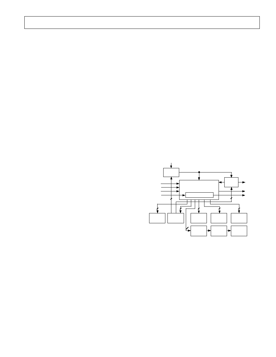
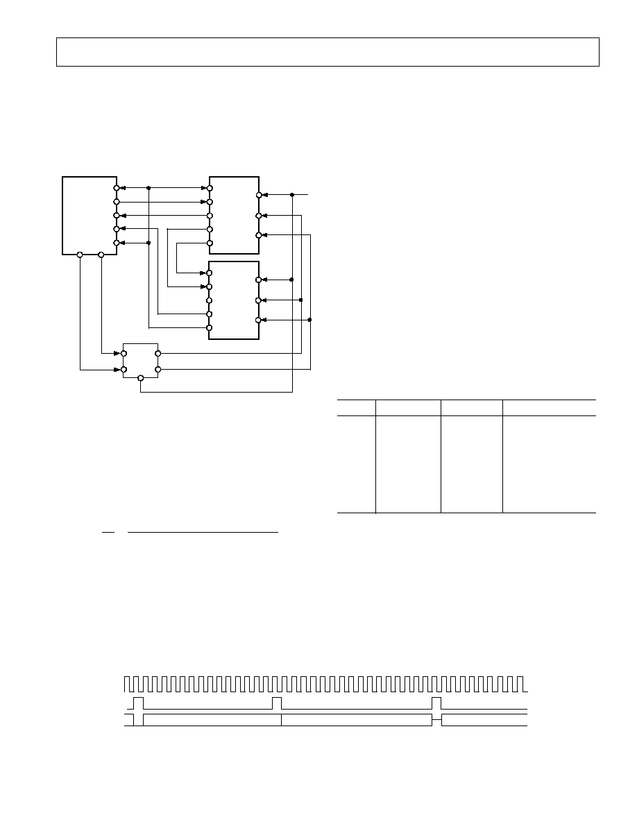
The SPORT block diagram, shown in Figure 9, details the blocks
associated with AD73360 including the eight control registers
(AH), external MCLK to internal DMCLK divider and serial
clock divider. The divider rates are controlled by the setting of
Control Register B. The AD73360 features a master clock
divider that allows users the flexibility of dividing externally
available high frequency DSP or CPU clocks to generate a lower
frequency master clock internally in the AD73360 which may be
more suitable for either serial transfer or sampling rate require-
ments. The master clock divider has five divider options (
÷1
default condition,
÷2, ÷3, ÷4, ÷5) that are set by loading the
master clock divider field in Register B with the appropriate
code (see Table VI). Once the internal device master clock
(DMCLK) has been set using the master clock divider, the
sample rate and serial clock settings are derived from DMCLK.
MCLK
DIVIDER
MCLK
(EXTERNAL)
SE
RESET
SDIFS
SDI
SERIAL PORT
(SPORT)
SERIAL REGISTER
SCLK
CONTROL
REGISTER
B
CONTROL
REGISTER
C
CONTROL
REGISTER
D
CONTROL
REGISTER
E
CONTROL
REGISTER
A
3
8
8
8
8
8
8
2
DMCLK
(INTERNAL)
SDOFS
SDO
CONTROL
REGISTER
F
CONTROL
REGISTER
G
CONTROL
REGISTER
H
SCLK
DIVIDER
Figure 9. SPORT Block Diagram
The SPORT can work at four different serial clock (SCLK)
rates: chosen from DMCLK, DMCLK/2, DMCLK/4 or
DMCLK/8, where DMCLK is the internal or device master
clock resulting from the external or pin master clock being di-
vided by the master clock divider. Care should be taken when
selecting Master Clock, Serial Clock and Sample Rate divider
settings to ensure that there is sufficient time to read all the data
from the AD73360 before the next sample interval.
REV. A
AD73360
14
SPORT Register Maps
There are eight control registers for the AD73360, each eight
bits wide. Table V shows the control register map for the
AD73360. The first two control registers, CRA and CRB, are
reserved for controlling the SPORT. They hold settings for
parameters such as bit rate, internal master clock rate and de-
vice count. If multiple AD73360s are cascaded, registers CRA
and CRB on each device must be programmed with the same
setting to ensure correct operation (this is shown in the pro-
gramming examples). The other six registers; CRC through
CRH are used to hold control settings for the Reference, Power
Control, ADC channel and PGA sections of the device. It is
not necessary that the contents of CRC through CRH on
each AD73360 are similar. Control registers are written to on
the negative edge of SCLK.
Table VI. Control Word Description
15
14
13
12
11
10
9
8
7
6
5
4
3
2
1
0
C/
D
R/
W
DEVICE ADDRESSS
REGISTER ADDRESS
REGISTER DATA
Control
Frame
Description
Bit 15
Control/
Data
When set high, it signifies a control word in Program or Mixed Program/Data Modes. When set
low, it signifies an invalid control word in Program Mode.
Bit 14
Read/
Write
When set low, it tells the device that the data field is to be written to the register selected by the
register field setting provided the address field is zero. When set high, it tells the device that the
selected register is to be written to the data field in the serial register and that the new control
word is to be output from the device via the serial output.
Bits 1311
Device Address
This 3-bit field holds the address information. Only when this field is zero is a device selected. If
the address is not zero, it is decremented and the control word is passed out of the device via the
serial output.
Bits 108
Register Address
This 3-bit field is used to select one of the eight control registers on the AD73360.
Bits 70
Register Data
This 8-bit field holds the data that is to be written to or read from the selected register provided
the address field is zero.
Table V. Control Register Map
Address (Binary)
Name
Description
Type
Width
Reset Setting (Hex)
000
CRA
Control Register A
R/
W
8
0x00
001
CRB
Control Register B
R/
W
8
0x00
010
CRC
Control Register C
R/
W
8
0x00
011
CRD
Control Register D
R/
W
8
0x00
100
CRE
Control Register E
R/
W
8
0x00
101
CRF
Control Register F
R/
W
8
0x00
110
CRG
Control Register G
R/
W
8
0x00
111
CRH
Control Register H
R/
W
8
0x00
REV. A
AD73360
15
Table VII. Control Register A Description
7
6
5
4
3
2
1
0
RESET
DC2
DC1
DC0
SLB
MM
DATA/
PGM
Bit Name
Description
0
DATA/
PGM
Operating Mode (0 = Program; 1 = Data Mode)
1
MM
Mixed Mode (0 = OFF; 1 = Enabled)
2
Reserved
Must Be Programmed to Zero (0)
3
SLB
SPORT Loop-Back Mode (0 = OFF; 1 = Enabled)
4
DC0
Device Count (Bit 0)
5
DC1
Device Count (Bit 1)
6
DC2
Device Count (Bit 2)
7
RESET
Software Reset (0 = OFF; 1 = Initiates Reset)
Table VIII. Control Register B Description
7
6
5
4
3
2
1
0
C E E
MCD2
MCD1
MCD0
SCD1
SCD0
DR1
DR0
Bit Name
Description
0
DR0
Decimation Rate (Bit 0)
1
DR1
Decimation Rate (Bit 1)
2
SCD0
Serial Clock Divider (Bit 0)
3
SCD1
Serial Clock Divider (Bit 1)
4
MCD0
Master Clock Divider (Bit 0)
5
MCD1
Master Clock Divider (Bit 1)
6
MCD2
Master Clock Divider (Bit 2)
7
CEE
Control Echo Enable (0 = OFF; 1 = Enabled)
Table IX. Control Register C Description
7
6
5
4
3
2
1
0
5VEN
RU
PUREF
GPU
Bit Name
Description
0
GPU
Global Power-Up Device (0 = Power Down; 1 = Power Up)
1
Reserved
Must Be Programmed to Zero (0)
2
Reserved
Must Be Programmed to Zero (0)
3
Reserved
Must Be Programmed to Zero (0)
4
Reserved
Must Be Programmed to Zero (0)
5
PUREF
REF Power (0 = Power Down; 1 = Power Up)
6
RU
REFOUT Use (0 = Disable REFOUT; 1 = Enable REFOUT)
7
5VEN
Enable 5 V Operating Mode (0 = Disable 5 V Mode;
1 = Enable 5 V Mode)
CONTROL REGISTER A
CONTROL REGISTER B
CONTROL REGISTER C
REV. A
AD73360
16
Table X. Control Register D Description
7
6
5
4
3
2
1
0
PUI2
I2GS2
I2GS1
I2GS0
PUI1
I1GS2
I1GS1
I1GS0
Bit Name
Description
0
I1GS0
ADC1:Input Gain Select (Bit 0)
1
I1GS1
ADC1:Input Gain Select (Bit 1)
2
I1GS2
ADC1:Input Gain Select (Bit 2)
3
PUI1
Power Control (ADC1); 1 = ON, 0 = OFF
4
I2GS0
ADC2:Input Gain Select (Bit 0)
5
I2GS1
ADC2:Input Gain Select (Bit 1)
6
I2GS2
ADC2:Input Gain Select (Bit 2)
7
PUI2
Power Control (ADC2); 1 = ON, 0 = OFF
Table XI. Control Register E Description
7
6
5
4
3
2
1
0
PUI4
I4GS2
I4GS1
I4GS0
PUI3
I3GS2
I3GS1
I3GS0
Bit Name
Description
0
I3GS0
ADC3:Input Gain Select (Bit 0)
1
I3GS1
ADC3:Input Gain Select (Bit 1)
2
I3GS2
ADC3:Input Gain Select (Bit 2)
3
PUI3
Power Control (ADC3); 1 = ON, 0 = OFF
4
I4GS0
ADC4:Input Gain Select (Bit 0)
5
I4GS1
ADC4:Input Gain Select (Bit 1)
6
I4GS2
ADC4:Input Gain Select (Bit 2)
7
PUI4
Power Control (ADC4); 1 = ON, 0 = OFF
Table XII. Control Register F Description
7
6
5
4
3
2
1
0
PUI6
I6GS2
I6GS1
I6GS0
PUI5
I5GS2
I5GS1
I5GS0
Bit Name
Description
0
I5GS0
ADC5:Input Gain Select (Bit 0)
1
I5GS1
ADC5:Input Gain Select (Bit 1)
2
I5GS2
ADC5:Input Gain Select (Bit 2)
3
PUI5
Power Control (ADC5); 1 = ON, 0 = OFF
4
I6GS0
ADC6:Input Gain Select (Bit 0)
5
I6GS1
ADC6:Input Gain Select (Bit 1)
6
I6GS2
ADC6:Input Gain Select (Bit 2)
7
PUI6
Power Control (ADC6); 1 = ON, 0 = OFF
CONTROL REGISTER D
CONTROL REGISTER E
CONTROL REGISTER F
REV. A
AD73360
17
Table XIII. Control Register G Description
7
6
5
4
3
2
1
0
SEEN
RMOD
CH6
CH5
CH4
CH3
CH2
CH1
Bit Name
Description
0
CH1
Channel 1 Select
1
CH2
Channel 2 Select
2
CH3
Channel 3 Select
3
CH4
Channel 4 Select
4
CH5
Channel 5 Select
5
CH6
Channel 6 Select
6
RMOD
Reset Analog Modulator
7
SEEN
Enable Single-Ended Input Mode
Table XIV. Control Register H Description
7
6
5
4
3
2
1
0
INV
TME
CH6
CH5
CH4
CH3
CH2
CH1
Bit Name
Description
0
CH1
Channel 1 Select
1
CH2
Channel 2 Select
2
CH3
Channel 3 Select
3
CH4
Channel 4 Select
4
CH5
Channel 5 Select
5
CH6
Channel 6 Select
6
TME
Test Mode Enable
7
INV
Enable Invert Channel Mode
CONTROL REGISTER G
CONTROL REGISTER H
REGISTER BIT DESCRIPTIONS
Control Register A
CRA:0
Data/Program Mode. This bit controls the operating mode of the AD73360. If CRA:1 is 0, then a 0 in this bit
places the part in Program Mode. If CRA:1 is 0, then a 1 in this bit places the part in Data Mode.
CRA:1
Mixed Mode. If this bit is a 0, then the operating mode is determined by CRA:0. If this bit is a 1, then the
part operates in Mixed Mode.
CRA:2
Reserved. This bit is reserved and should be programmed to 0 to ensure correct operation.
CRA:3
SPORT Loop Back. This is a diagnostic mode. This bit should be set to 0 to ensure correct operation.
CRA:46
Device Count Bits. These bits tell the AD73360 how many devices are used in a cascade. All devices in the
cascade should be programmed to the same value ensure correct operation. See Table XVIII.
CRA:7
Reset. Writing a 1 to this bit will initiate a software reset of the AD73360.
Control Register B
CRB:01
Decimation Rate. These bits are used to set the decimation of the AD73360. See Table VII.
CRB:23
Serial Clock Divider. These bits are used to set the serial clock frequency. See Table VI.
CRB:46
Master Clock Divider. These bits are used to set the Master Clock Divider ratio. See Table V.
CRB:7
Control Echo Enable. Setting this bit to a 1 will cause the AD73360 to write out any control words it receives.
This is used as a diagnostic mode. This bit should be set to 0 for correct operation in Mixed Mode or Data Mode.

REV. A
AD73360
18
Control Register C
CRC:0
Global Power-Up. Writing a 1 to this bit will cause all six channels of the AD73360 to power-up regardless of the
status of the Power Control Bits in CRD-CRF. If less than six channels are required, this bit should be set to 0 and
the Power Control Bits of the relevant channels should be set to 1.
CRC:14
Reserved. These bits are reserved and should be programmed to 0 to ensure correct operation.
CRC:5
Power-Up Reference. This bit controls the state of the on-chip reference. A 1 in this bit will power up the refer-
ence. A 0 in this bit will power-down the reference. Note that the reference is automatically powered up if any
channel is enabled.
CRC:6
Reference Output. When this bit is set to 1, the REFOUT pin is enabled.
CRC:7
5 V Enable. When this bit is set to 1, the 5 V operating mode is enabled.
Control Register D
CRD:02
Input Gain Selection. These bits select the input gain for ADC1. See Table IV.
CRD:3
Power Control for ADC1. A 1 in this bit powers up ADC1.
CRD:46
Input Gain Selection. These bits select the input gain for ADC2. See Table IV.
CRD:7
Power Control for ADC2. A 1 in this bit powers up ADC2.
Control Register E
CRE:0-2
Input Gain Selection. These bits select the input gain for ADC3. See Table IV.
CRE:3
Power Control for ADC3. A 1 in this bit powers up ADC3.
CRE:46
Input Gain Selection. These bits select the input gain for ADC4. See Table IV.
CRE:7
Power Control for ADC4. A 1 in this bit powers up ADC4.
Control Register F
CRF:02
Input Gain Selection. These bits select the input gain for ADC5. See Table IV.
CRF:3
Power Control for ADC5. A 1 in this bit powers up ADC5.
CRF:46
Input Gain Selection. These bits select the input gain for ADC6. See Table IV.
CRF:7
Power Control for ADC6. A 1 in this bit powers up ADC6.
Control Register G
CRG:05
Channel Select. These bits are used in association with CRG:6 and CRG:7. If the Reset Analog Modulator bit
(CRG:6) is 1, then a 1 in a Channel Select bit location will reset the Analog Modulator for that channel. If the
Single-Ended Enable Mode bit (CRG:7) is 1, then a 1 in a Channel Select bit location will put that channel into
Single-Ended Mode. If any channel has its Channel Select bit set to 0, the channel will be set for Differentially-
Ended Mode and will not have its analog modulator reset regardless of the state of CRG:6 and CRG:7.
CRG:6
Reset Analog Modulator. Setting this bit to a 1 will reset the Analog Modulators for any channel whose Channel
Select bit (CRG:05) is set to 1. This bit should be set to 0 for normal operation.
CRG:7
Single-Ended Enable Mode. Setting this bit to a 1 will enable Single-Ended Mode on any channel whose Channel
Select bit (CRG:05) is set to 1. Setting this bit to 0 will select Differentially-Ended Input Mode for all channels.
Control Register H
CRH:05
Invert Select. These bits are used in association with CRH:7. If the Enable Invert Channel Mode bit (CRH:7) is 1,
then a 1 in a Channel Select bit location will put that channel into Inverted Mode. If any channel has its Channel
Select bit set to 0, the channel will not be inverted regardless of the state CRH:7.
CRH:6
Test Mode Enable. This bit should be set to 0 to ensure normal operation.
CRH:7
Enable Invert Channel Mode. Setting this bit to a 1 will enable invert any channel whose Channel Select bit
(CRH:05) is set to 1. Setting this bit to 0 will select Noninverted (Normal) Mode for all channels.
REV. A
AD73360
19
Master Clock Divider
The AD73360 features a programmable master clock divider
that allows the user to reduce an externally available master
clock, at pin MCLK, by one of the ratios 1, 2, 3, 4 or 5 to pro-
duce an internal master clock signal (DMCLK) that is used to
calculate the sampling and serial clock rates. The master clock
divider is programmable by setting CRB:4-6. Table XV shows
the division ratio corresponding to the various bit settings. The
default divider ratio is divide-by-one.
Table XV. DMCLK (Internal) Rate Divider Settings
MCD2
MCD1
MCD0
DMCLK Rate
0
0
0
MCLK
0
0
1
MCLK/2
0
1
0
MCLK/3
0
1
1
MCLK/4
1
0
0
MCLK/5
1
0
1
MCLK
1
1
0
MCLK
1
1
1
MCLK
Serial Clock Rate Divider
The AD73360 features a programmable serial clock divider that
allows users to match the serial clock (SCLK) rate of the data to
that of the DSP engine or host processor. The maximum SCLK
rate available is DMCLK and the other available rates are:
DMCLK/2, DMCLK/4 and DMCLK/8. The slowest rate
(DMCLK/8) is the default SCLK rate. The serial clock divider
is programmable by setting bits CRB:23. Table XVI shows the
serial clock rate corresponding to the various bit settings.
Table XVI. SCLK Rate Divider Settings
SCD1
SCD0
SCLK Rate
0
0
DMCLK/8
0
1
DMCLK/4
1
0
DMCLK/2
1
1
DMCLK
Decimation Rate Divider
The AD73360 features a programmable decimation rate divider
that allows users flexibility in matching the AD73360's ADC
sample rates to the needs of the DSP software. The maximum
sample rate available is DMCLK/256 and the other available
rates are: DMCLK/512, DMCLK/1024 and DMCLK/2048.
The slowest rate (DMCLK/2048) is the default sample rate.
The sample rate divider is programmable by setting bits CRB:0-1.
Table XVII shows the sample rate corresponding to the various
bit settings.
Table XVII. Decimation Rate Divider Settings
DR1
DR0
Sample Rate
0
0
DMCLK/2048
0
1
DMCLK/1024
1
0
DMCLK/512
1
1
DMCLK/256
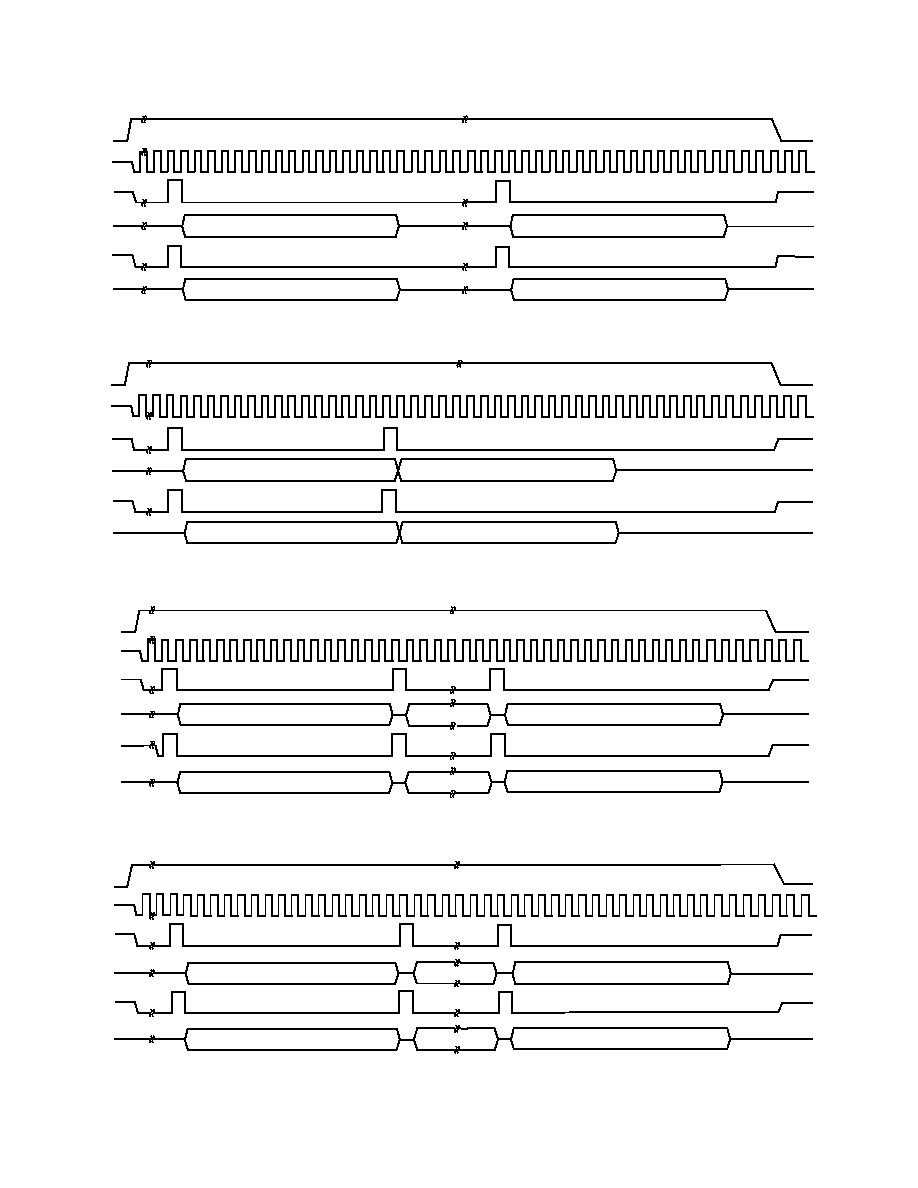
OPERATION
General Description
The AD73360 inputs and outputs data in a Time Division
Multiplexing (TDM) format. When data is being read from the
AD73360 each channel has a fixed time slot in which its data is
transmitted. If a channel is not powered up, no data is transmit-
ted during the allocated time slot and the SDO line will be
three-stated. When the AD73360 is first powered up or reset it
will be set to Program Mode and will output an SDOFS. After a
reset the SDOFS will be asserted once every sample period
(125
µs assuming 16.384 MHz master clock). If the AD73360 is
configured in Frame Sync Loop-Back Mode, one control word
can be transmitted after each SDOFS pulse. Figure 10a shows
the SDO and SDOFS lines after a reset. The serial data sent by
SDO will not contain valid ADC data until the AD73360 is put
into Data Mode or Mixed Mode. Control Registers D through
F allow channels to be powered up individually. This gives
greater flexibility and control over power consumption. Figure
10b shows the SDOFS and SDO of the AD73360 when all
channels are powered up and Figure 10c shows SDOFS and
SDO with channels 1, 3 and 5 powered up.
SDOFS
SDO
SE
1/F
SAMPLE
Figure 10a. Output Timing After Reset (Program Mode)
SDOFS
SDO
SE
CHANNEL 1
CHANNEL 2
CHANNEL 3
CHANNEL 4
CHANNEL 5
CHANNEL 6
Figure 10b. Output Timing: All Channels Powered Up (Data/Mixed Mode)
SDOFS
SDO
SE
CHANNEL 5
CHANNEL 1
CHANNEL 3
Figure 10c. Output Timing: Channels 1, 3 and 5 Powered Up (Data/Mixed Mode)

REV. A
AD73360
20
Resetting the AD73360
The
RESET pin resets all the control registers. All registers are
reset to zero indicating that the default SCLK rate (DMCLK/8)
and sample rate (DMCLK/2048) are at a minimum to ensure
that slow speed DSP engines can communicate effectively. As
well as resetting the control registers using the
RESET pin, the
device can be reset using the
RESET bit (CRA:7) in Control
Register A. Both hardware and software resets require four
DMCLK cycles. On reset, DATA/
PGM (CRA:0) is set to 0
(default condition) thus enabling Program Mode. The reset
conditions ensure that the device must be programmed to the
correct settings after power-up or reset. Following a reset, the
SDOFS will be asserted approximately 2070 master (MCLK)
cycles after
RESET goes high. The data that is output following
the reset and during Program Mode is random and contains no
valid information until either data or mixed mode is set.
Power Management
The individual functional blocks of the AD73360 can be en-
abled separately by programming the power control register
CRC. It allows certain sections to be powered down if not re-
quired, which adds to the device's flexibility in that the user
need not incur the penalty of having to provide power for a
certain section if it is not necessary to their design. The power
control registers provide individual control settings for the major
functional blocks on each analog front end unit and also a global
override that allows all sections to be powered up/down by
setting/clearing the bit. Using this method the user could, for
example, individually enable a certain section, such as the refer-
ence (CRC:5), and disable all others. The global power-up
(CRC:0) can be used to enable all sections but if power-down is
required using the global control, the reference will still be en-
abled; in this case, because its individual bit is set. Refer to
Table XII for details of the settings of CRC. CRDCRF can be
used to control the power status of individual channels allowing
multiple channels to be powered down if required.
Operating Modes
There are three operating modes available on the AD73360.
They are Program, Data and Mixed Program/Data. The device
configuration--register settings--can be changed only in Pro-
gram and Mixed Program/Data Modes. In all modes, transfers
of information to or from the device occur in 16-bit packets,
therefore the DSP engine's SPORT will be programmed for 16-
bit transfers.
Program (Control) Mode
In Program Mode, CRA:0 = 0, the user writes to the control
registers to set up the device for desired operation--SPORT
operation, cascade length, power management, input/output
gain, etc. In this mode, the 16-bit information packet sent to the
device by the DSP engine is interpreted as a control word whose
format is shown in Table VI. In this mode, the user must ad-
dress the device to be programmed using the address field of the
control word. This field is read by the device and if it is zero
(000 bin), the device recognizes the word as being addressed to it.
If the address field is not zero, it is then decremented and the
control word is passed out of the device--either to the next
device in a cascade or back to the DSP engine. This 3-bit ad-
dress format allows the user to uniquely address any one of up
to eight devices in a cascade. If the AD73360 is used in a stand-
alone configuration connected to a DSP, the device address
corresponds to 0. If, on the other hand, the AD73360 is config-
ured in a cascade of multiple devices, its device address corre-
sponds with its hardwired position in the cascade.
Following reset, when the SE pin is enabled, the AD73360
responds by raising the SDOFS pin to indicate that an output
sample event has occurred. Control words can be written to the
device to coincide with the data being sent out of the SPORT, as
shown in Figure 12 (Directly Coupled), or they can lag the out-
put words by a time interval that should not exceed the sample
interval (Indirectly Coupled). Refer to the Digital Interface
section for more information. After reset, output frame sync
pulses will occur at a slower default sample rate, which is DM-
CLK/2048, until Control Register B is programmed, after which
the SDOFS will be pulsed at the selected rate. This is to allow
slow controller devices to establish communication with the
AD73360. During Program Mode, the data output by the de-
vice is random and should not be interpreted as ADC data.
Data Mode
Once the device has been configured by programming the cor-
rect settings to the various control registers, the device may exit
Program Mode and enter Data Mode. This is done by program-
ming the DATA/
PGM (CRA:0) bit to a 1 and MM (CRA:1) to
0. Once the device is in Data Mode, the input data is ignored.
When the device is in normal Data Mode (i.e., mixed mode
disabled), it must receive a hardware reset to reprogram any of
the control register settings.
Appendix C details the initialization and operation of an analog
front end cascade in normal Data Mode.
Mixed Program/Data Mode
This mode allows the user to send control words to the device
while receiving ADC words. This permits adaptive control of
the device whereby control of the input gains can be affected by
reprogramming the control registers. The standard data frame
remains 16 bits, but now the MSB is used as a flag bit to indi-
cate that the remaining 15 bits of the frame represents control
information. Mixed mode is enabled by setting the MM bit
(CRA:1) to 1 and the DATA/
PGM bit (CRA:0) to 1. In the
case where control setting changes will be required during nor-
mal operation, this mode allows the ability to load control infor-
mation with the slight inconvenience of formatting the data.
Note that the output samples from the ADC will also have the
MSB set to zero to indicate it is a data word.
A description of a single device operating in mixed mode is
detailed in Appendix B, while Appendix D details the initializa-
tion and operation of an analog front end cascade operating in
mixed mode. Note that it is not essential to load the control
registers in Program Mode before setting mixed mode active.
Mixed mode may be selected with the first write by program-
ming CRA and then transmitting other control words.
REV. A
AD73360
21
INTERFACING
The AD73360 can be interfaced to most modern DSP engines
using conventional serial port connections and an extra enable
control line. Both serial input and output data use an accompa-
nying frame synchronization signal which is active high one
clock cycle before the start of the 16-bit word or during the last
bit of the previous word if transmission is continuous. The serial
clock (SCLK) is an output from the AD73360 and is used to
define the serial transfer rate to the DSP's Tx and Rx ports.
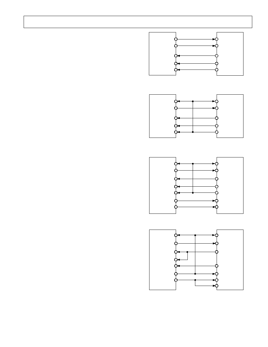
Two primary configurations can be used: the first is shown in
Figure 11 where the DSP's Tx data, Tx frame sync, Rx data and
Rx frame sync are connected to the AD73360's SDI, SDIFS,
SDO and SDOFS respectively. This configuration, referred to
as indirectly coupled or nonframe sync loop-back, has the effect
of decoupling the transmission of input data from the receipt of
output data. When programming the DSP serial port for this
configuration, it is necessary to set the Rx frame sync as an
input to the DSP and the Tx frame sync as an output generated
by the DSP. This configuration is most useful when operating in
mixed mode, as the DSP has the ability to decide how many
words can be sent to the AD73360(s). This means that full con-
trol can be implemented over the device configuration in a given
sample interval. The second configuration (shown in Figure 12)
has the DSP's Tx data and Rx data connected to the AD73360's
SDI and SDO, respectively, while the DSP's Tx and Rx frame
syncs are connected to the AD73360's SDIFS and SDOFS. In
this configuration, referred to as directly coupled or frame sync
loop-back, the frame sync signals are connected together and
the input data to the AD73360 is forced to be synchronous with
the output data from the AD73360. The DSP must be pro-
grammed so that both the Tx and Rx frame syncs are inputs as
the AD73360's SDOFS will be input to both. This configura-
tion guarantees that input and output events occur simulta-
neously and is the simplest configuration for operation in normal
Data Mode. Note that when programming the DSP in this
configuration it is advisable to preload the Tx register with the
first control word to be sent before the AD73360 is taken out of
reset. This ensures that this word will be transmitted to coincide
with the first output word from the device(s).
Digital Interfacing
The AD73360 is designed to easily interface to most common
DSPs. The SCLK, SDO, SDOFS, SDI and SDIFS must be
connected to the SCLK, DR, RFS, DT and TFS pins of the
DSP respectively. The SE pin may be controlled from a parallel
output pin or flag pin such as FL02 on the ADSP-21xx (or XF
on the TMS320C5x) or, where SPORT power-down is not
required, it can be permanently strapped high using a suitable
pull-up resistor. The
RESET pin may be connected to the sys-
tem hardware reset structure or it may also be controlled using a
dedicated control line. In the event of tying it to the global
system reset, it is necessary to operate the device in mixed
mode, which allows a software reset, otherwise there is no con-
venient way of resetting the device. Figures 11 and 12 show
typical connections to an ADSP-2181 while Figures 13 and 14
show typical connections to an ADSP-21xx and a TMS320C5x,
respectively.
TFS
DT
SCLK
DR
RFS
ADSP-21xx
DSP
AD73360
SDIFS
SDI
SCLK
SDO
SDOFS
Figure 11. Indirectly Coupled or Nonframe Sync Loop-
Back Configuration
TFS
DT
SCLK
DR
RFS
ADSP-21xx
DSP
AD73360
SDIFS
SDI
SCLK
SDO
SDOFS
Figure 12. Directly Coupled or Frame Sync Loop-
Back Configuration
TFS
DT
SCLK
DR
RFS
ADSP-21xx
DSP
AD73360
ANALOG
FRONT-END
SDIFS
SDI
SCLK
SDO
SDOFS
FL0
FL1
RESET
SE
Figure 13. AD73360 Connected to ADSP-21xx
FSX
DX
CLKX
CLKR
DR
TMS320C5x
DSP
AD73360
ANALOG
FRONT-END
SDIFS
SDI
SCLK
SDO
SDOFS
FSR
XF
RESET
SE
Figure 14. AD73360 Connected to TMS320C5x
REV. A
AD73360
22
SE
SDI
CONTROL WORD
CONTROL WORD
SDIFS
UNDEFINED DATA
SDO
UNDEFINED DATA
SDOFS
SCLK
Figure 15a. Interface Signal Timing for Program Mode Operation (Writing to a Register)
SE
SCLK
SDIFS
SDI
REGISTER READ INSTRUCTION
0x7FFF OR CONTROL WORD
UNDEFINED DATA
SDO
READ RESULT
SDOFS
Figure 15b. Interface Signal Timing for Program Mode Operation (Reading a Register)
SE
SDOFS
SCLK
SDIFS
SDI
CONTROL WORD
CONTROL WORD
CHANNEL 1 ADC SAMPLE WORD
SDO
CHANNEL 6 ADC SAMPLE WORD
Figure 16a. Interface Signal Timing for Mixed Mode Operation
SE
SDOFS
SCLK
SDIFS
SDI
DON'T CARE
DON'T CARE
CHANNEL 1 ADC SAMPLE WORD
SDO
CHANNEL 6 ADC SAMPLE WORD
Figure 16b. Interface Signal Timing for Data Mode Operation
REV. A
AD73360
23
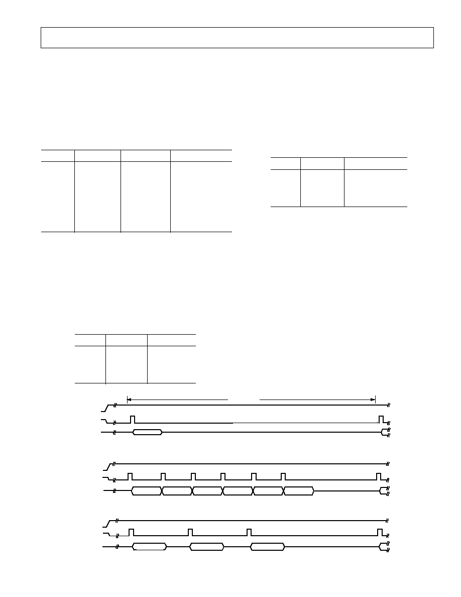
Cascade Operation
The AD73360 has been designed to support up to eight devices
in a cascade connected to a single serial port (see Figure 17).
The SPORT interface protocol has been designed so that device
addressing is built into the packet of information sent to the
device. This allows the cascade to be formed with no extra hard-
ware overhead for control signals or addressing. A cascade can
be formed in either of the two modes previously discussed.
TFS
DT
DR
RFS
AD73360
SDIFS
SDI
SCLK
SDO
SDOFS
SCLK
DEVICE 1
MCLK
SE
RESET
AD73360
74HC74
Q0
Q1
D1
D0
FL0
FL1
ADSP-2181
DSP
CLK
SDIFS
SDI
SCLK
SDO
SDOFS
DEVICE 2
MCLK
SE
RESET
Figure 17. Connection of Two AD73360s Cascaded to
ADSP-2181
There may be some restrictions in cascade operation due to the
number of devices configured in the cascade and the serial clock
rate chosen. The formula below gives an indication of whether
the combination of sample rate, serial clock and number of
devices can be successfully cascaded. This assumes a directly
coupled frame sync arrangement as shown in Figure 12 and does
not take any interrupt latency into account.
1
6
1
16
17
f
Device Count
SCLK
S
×
- ×
+
[((
)
)
]
When using the indirectly coupled frame sync configuration in
cascaded operation it is necessary to be aware of the restrictions
in sending control word data to all devices in the cascade. The
user should ensure that there is sufficient time for all the control
words to be sent between reading the last ADC sample and the
start of the next sample period.
In Cascade Mode, each device must know the number of de-
vices in the cascade to be able to output data at the correct
time. Control Register A contains a 3-bit field (DC02) that is
programmed by the DSP during the programming phase. The
default condition is that the field contains 000b, which is equiva-
lent to a single device in cascade (see Table XVIII). However,
for cascade operation this field must contain a binary value that
is one less than the number of devices in the cascade. With a
number of AD73360s in cascade each device takes a turn to
send an ADC result to the DSP. For example, in a cascade of
two devices the data will be output as Device 2-Channel 1,
Device 1-Channel 1, Device 2-Channel 2, Device 1-Channel 2
etc. When the first device in the cascade has transmitted its
channel data there is an additional SCLK period during which
the last device asserts its SDOFS as it begins its transmission of
the next channel. This will not cause a problem for most DSPs
as they count clock edges after a frame sync and hence the
extra bit will be ignored.
When multiple devices are connected in cascade there are also
restrictions concerning which ADC channels can be powered
up. In all cases the cascaded devices must all have the same
channels powered up (i.e., for a cascade of two devices requir-
ing Channels 1 and 2 on Device 1 and Channel 5 on Device 2,
Channels 1, 2 and 5 must be powered up on both devices to
ensure correct operation). Figure 18 shows the timing se-
quence for two devices in cascade.
Table XVIII. Device Count Settings
DC2
DC1
DC0
Cascade Length
0
0
0
1
0
0
1
2
0
1
0
3
0
1
1
4
1
0
0
5
1
0
1
6
1
1
0
7
1
1
1
8
Connection of a cascade of devices to a DSP, as shown in
Figure 17, is no more complicated than connecting a single
device. Instead of connecting the SDO and SDOFS to the
DSP's Rx port, these are now daisy-chained to the SDI and
SDIFS of the next device in the cascade. The SDO and
SDOFS of the final device in the cascade are connected to the
DSP's Rx port to complete the cascade. SE and
RESET on all
devices are fed from the signals that were synchronized with
the MCLK using the circuit of Figure 19. The SCLK from
only one device need be connected to the DSP's SCLK input(s)
as all devices will be running at the same SCLK frequency and
phase.
1
2
3
4 5
6 7
8 9
10 11 12 13 14 15 16 1
2
3
4 5
6
7 8 9 10 11 12 13 14 15 16 17
DEVICE 2 - CHANNEL 1
DEVICE 1 - CHANNEL 1
1
2
3
4 5
6 7
8
DEVICE 2 - CHANNEL 2
Figure 18. Cascade Timing for a Two-Device Cascade
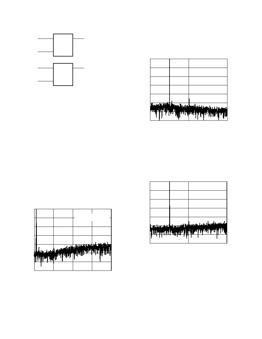
REV. A
AD73360
24
1/2
74HC74
CLK
D
Q
DSP CONTROL
TO SE
MCLK
SE SIGNAL SYNCHRONIZED
TO MCLK
1/2
74HC74
CLK
D
Q
DSP CONTROL
TO
RESET
MCLK
RESET SIGNAL SYNCHRONIZED
TO MCLK
Figure 19. SE and
RESET Sync Circuit for Cascaded
Operation
PERFORMANCE
As the AD73360 is designed to provide high performance, low
cost conversion, it is important to understand the means by
which this high performance can be achieved in a typical appli-
cation. This section will, by means of spectral graphs, outline
the typical performance of the device and highlight some of the
options available to users in achieving their desired sample rate,
either directly in the device or by doing some post-processing in
the DSP, while also showing the advantages and disadvantages
of the different approaches.
Encoder Section
The encoder section samples at DMCLK/256, which gives a
64 kHz output rate for DMCLK equal to 16.384 MHz. The
noise-shaping of the sigma-delta modulator also depends on the
frequency at which it is clocked, which means that the best
dynamic performance in a particular bandwidth is achieved by
oversampling at the highest possible rate. If we assume that the
signals of interest are in the voice bandwidth of dc4 kHz, then
sampling at 64 kHz gives a spectral response which ensures
good SNR performance in the voice bandwidth, as shown in
Figure 20.
FREQUENCY
kHz
0
0
dBs
20
8
16
24
32
100
140
120
40
60
80
SNR = 59.0dB (DC TO f
S
/2)
SNR = 80.8dB (DC TO 4kHz)
Figure 20. FFT (ADC 64 kHz Sampling)
The sampling rate can be varied by programming the Decimation
Rate Divider settings in CRB. For a DMCLK of 16.384 MHz
sample rates of 64 kHz, 32 kHz, 16 kHz and 8 kHz are available.
Figure 21 shows the final spectral response of a signal sampled
at 8 kHz using the maximum oversampling rate.
FREQUENCY
kHz
0
0
dBs
20
2
4
100
140
120
40
60
80
SNR = 80dBs (DC TO 4kHz)
Figure 21. FFT (ADC 8 kHz Internally Decimated from
64 kHz)
It is possible to generate lower sample rates through reducing
the oversampling ratio by programming the DMCLK Rate
Divider Settings in CRB (MCD2-MCD1) This will have the
effect of spreading the quantization noise over a lesser band-
width resulting in a degradation of dynamic performance.
Figure 22 shows a FFT plot of a signal sampled at 8 kHz rate
produced by reducing the DMCLK Rate.
FREQUENCY
kHz
0
0
dBs
20
2
4
100
140
120
40
60
80
SNR = 72.2dBs (DC TO f
S
/2)
Figure 22. FFT (ADC 8 kHz Sampling with Reduced
DMCLK Rate)
REV. A
AD73360
25
Figure 23 shows a comparison of SNR results achieved by vary-
ing either the Decimation Rate Setting or the DMCLK Rate
Settings.
SAMPLING FREQUENCY
kHz
8
SNR
dBs
71
REDUCED
DMCLK
DMCLK = MCLK
72
73
74
75
76
77
78
79
80
81
16
24
32
40
48
56
64
Figure 23. Comparison of DMCLK and Decimation Rate
Settings
Encoder Group Delay
The AD73360 implementation offers a very low level of group
delay, which is given by the following relationship:
Group Delay (Decimator) = Order
× ((M1)/2) × Tdec
where:
Order is the order of the decimator (= 3),
M is the decimation factor (= 32) and
Tdec is the decimation sample interval (= 1/2.048e6)
=> Group Delay (Decimator) = 3
× (321)/2 × (1/2.048e6)
= 22.7
µs
If final filtering is implemented in the DSP, the final filter's
group delay must be taken into account when calculating overall
group delay.
DESIGN CONSIDERATIONS
Analog Inputs
The AD73360 features six signal conditioning inputs. Each
signal conditioning block allows the AD73360 to be used with
either a single-ended or differential signal. The applied signal
can also be inverted internally by the AD73360 if required. The
analog input signal to the AD73360 can be dc-coupled, pro-
vided that the dc bias level of the input signal is the same as the
internal reference level (REFOUT). Figure 24 shows the recom-
mended differential input circuit for the AD73360. The circuit
of Figure 24 implements first-order low-pass filters with a 3 dB
VIN
TO INPUT BIAS
CIRCUITRY
VINPx
VINNx
REFOUT
REFCAP
VOLTAGE
REFERENCE
0.047 F
0.047 F
100
100
0.1 F
Figure 24. Example Circuit for Differential Input
(DC Coupling)
point at 34 kHz; these are the only filters that must be imple-
mented external to the AD73360 to prevent aliasing of the
sampled signal. Since the ADC uses a highly oversampled ap-
proach that transfers the bulk of the antialiasing filtering into the
digital domain, the off-chip antialiasing filter need only be of a
low order. It is recommended that for optimum performance the
capacitors used for the antialiasing filter be of high quality di-
electric (NPO).
The AD73360's on-chip 38 dB preamplifier can be enabled
when there is not enough gain in the input circuit; the preampli-
fier is configured by bits IGS02 of CRD. The total gain must
be configured to ensure that a full-scale input signal produces a
signal level at the input to the sigma-delta modulator of the
ADC that does not exceed the maximum input range.
The dc biasing of the analog input signal is accomplished with
an on-chip voltage reference. If the input signal is not biased at
the internal reference level (via REFOUT), then it must be
ac-coupled with external coupling capacitors. CIN should be
0.1
µF or larger. The dc biasing of the input can then be accom-
plished using resistors to REFOUT as in Figure 25.
VIN
TO INPUT BIAS
CIRCUITRY
VINPx
VINNx
REFOUT
REFCAP
VOLTAGE
REFERENCE
0.047 F
100
100
CIN
CIN
10k
10k
0.047 F
0.1 F
Figure 25. Example Circuit for Differential Input
(AC Coupling)
Figures 26 and 27 detail ac- and dc-coupled input circuits for
single-ended operation respectively.
VIN
VINPx
VINNx
REFOUT
REFCAP
VOLTAGE
REFERENCE
100
CIN
10k
0.047 F
0.1 F
Figure 26. Example Circuit for Single-Ended Input
(AC Coupling)
VIN
VINPx
VINNx
REFOUT
REFCAP
VOLTAGE
REFERENCE
100
0.047 F
0.1 F
Figure 27. Example Circuit for Single-Ended Input
(DC Coupling)
REV. A
AD73360
26
Digital Interface
As there are a number of variations of sample rate and clock
speeds that can be used with the AD73360 in a particular appli-
cation, it is important to select the best combination to achieve
the desired performance. High speed serial clocks will read the
data from the AD73360 in a shorter time, giving more time for
processing by at the expense of injecting some digital noise into
the circuit. Digital noise can also be reduced by connecting
resistors (typ <50
) in series with the digital input and output
lines. The noise can be minimized by good grounding and lay-
out. Typically the best performance is achieved by selecting the
slowest sample rate and SCLK frequency for the required appli-
cation as this will produce the least amount of digital noise.
Figure 28 shows combinations of sample rate and SCLK fre-
quency which will allow data to be read from all six channels in
one sample period. These figures correspond to setting DMCLK =
MCLK.
8KSPS
16KSPS
32KSPS
64KSPS
SAMPLE RATE
SCLK
NOTE: SOME COMBINATIONS OF SCLK AND SAMPLE RATE WILL NOT
BE SUFFICIENT TO READ DATA FROM ALL SIX CHANNELS IN THE
ALLOTTED TIME. THESE ARE DEPICTED AS NO.
2MHz
YES
YES
NO
NO
4MHz
YES
YES
YES
NO
8MHz
YES
YES
YES
YES
16MHz
YES
YES
YES
YES
Figure 28. SCLK and Sample Rates
Grounding and Layout
Since the analog inputs to the AD73360 are differential, most of
the voltages in the analog modulator are common-mode volt-
ages. The excellent common-mode rejection of the part will
remove common-mode noise on these inputs. The analog and
digital supplies of the AD73360 are independent and separately
pinned out to minimize coupling between analog and digital
sections of the device. The digital filters on the encoder section
will provide rejection of broadband noise on the power supplies,
except at integer multiples of the modulator sampling frequency.
The digital filters also remove noise from the analog inputs
provided the noise source does not saturate the analog modula-
tor. However, because the resolution of the AD73360's ADC is
high, and the noise levels from the AD73360 are so low, care
must be taken with regard to grounding and layout.
The printed circuit board that houses the AD73360 should be
designed so the analog and digital sections are separated and
confined to certain sections of the board. The AD73360 pin
configuration offers a major advantage in that its analog and
digital interfaces are connected on opposite sides of the package.
This facilitates the use of ground planes that can be easily sepa-
rated, as shown in Figure 29. A minimum etch technique is
generally best for ground planes as it gives the best shielding.
Digital and analog ground planes should be joined in only one
place. If this connection is close to the device, it is recommended
to use a ferrite bead inductor as shown in Figure 29.
DIGITAL GROUND
ANALOG GROUND
Figure 29. Ground Plane Layout
Avoid running digital lines under the device for they will couple
noise onto the die. The analog ground plane should be allowed
to run under the AD73360 to avoid noise coupling. The power
supply lines to the AD73360 should use as large a trace as pos-
sible to provide low impedance paths and reduce the effects of
glitches on the power supply lines. Fast switching signals such as
clocks should be shielded with digital ground to avoid radiating
noise to other sections of the board, and clock signals should
never be run near the analog inputs. Traces on opposite sides of
the board should run at right angles to each other. This will
reduce the effects of feedthrough through the board. A microstrip
technique is by far the best but is not always possible with a
double-sided board. In this technique, the component side of
the board is dedicated to ground planes while signals are placed
on the other side.
Good decoupling is important when using high speed devices.
All analog and digital supplies should be decoupled to AGND
and DGND respectively, with 0.1
µF ceramic capacitors in
parallel with 10
µF tantalum capacitors. To achieve the best
from these decoupling capacitors, they should be placed as close
as possible to the device, ideally right up against it. In systems
where a common supply voltage is used to drive both the AVDD
and DVDD of the AD73360, it is recommended that the system's
AVDD supply be used. This supply should have the recom-
mended analog supply decoupling between the AVDD pins of
the AD73360 and AGND and the recommended digital supply
decoupling capacitors between the DVDD pin and DGND.
DSP Programming Considerations
This section discusses some aspects of how the serial port of the
DSP should be configured and the implications of whether Rx
and Tx interrupts should be enabled.
DSP SPORT Configuration
Following are the key settings of the DSP SPORT required for
the successful operation with the AD73360:
· Configure for external SCLK.
· Serial Word Length = 16 bits.
· Transmit and Receive Frame Syncs required with every word.
· Receive Frame Sync is an input to the DSP.
· Transmit Frame Sync is an:
Input--in Frame Sync Loop-Back Mode
Output--in Nonframe Sync Loop-Back Mode.
· Frame Syncs occur one SCLK cycle before the MSB of the
serial word.
· Frame Syncs are active high.
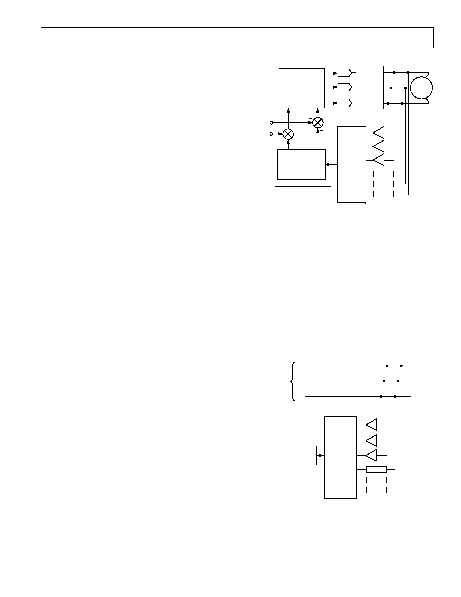
REV. A
AD73360
27
DSP SPORT Interrupts
If SPORT interrupts are enabled, it is important to note that the
active signals on the frame sync pins do not necessarily corre-
spond with the positions in time of where SPORT interrupts are
generated.
On ADSP-21xx processors, it is necessary to enable SPORT
interrupts and use Interrupt Service Routines (ISRs) to handle
Tx/Rx activity, while on the TMS320C5x processors it is pos-
sible to poll the status of the Rx and Tx registers, which means
that Rx/Tx activity can be monitored using a single ISR that
would ideally be the Tx ISR as the Tx interrupt will typically
occur before the Rx ISR.
APPLICATIONS EXAMPLES
Vector Motor Control
The current drawn by a motor can be split into two compo-
nents: one produces torque and the other produces magnetic
flux. For optimal performance of the motor, these two compo-
nents should be controlled independently. In conventional
methods of controlling a three-phase motor, the current (or
voltage) supplied to the motor and the frequency of the drive are
the basic control variables. However, both the torque and flux
are functions of current (or voltage) and frequency. This cou-
pling effect can reduce the performance of the motor because,
for example, if the torque is increased by increasing the fre-
quency, the flux tends to decrease.
Vector control of an ac motor involves controlling phase in
addition to drive and current frequency. Controlling the phase
of the motor requires feedback information on the position of
the rotor relative to the rotating magnetic field in the motor.
Using this information, a vector controller mathematically trans-
forms the three-phase drive currents into separate torque and
flux components. The AD73360, with its six-channel simulta-
neous sampling capability, is ideally suited for use in vector
motor control applications.
A block diagram of a vector motor control application using the
AD73360 is shown in Figure 30. The position of the field is
derived by determining the current in each phase of the motor.
V
IN1
, V
IN2
and V
IN3
of the AD73360 are used to digitize this
information.
Simultaneous sampling is critical to maintain the relative phase
information between the channels. A current-sensing isolation
amplifier, transformer or Hall-effect sensor is used between the
motor and the AD73360. Rotor information is obtained by
measuring the voltage from the three inputs to the motor. V
IN4
,
V
IN5
and V
IN6
of the AD73360 are used to obtain this informa-
tion. A DSP microprocessor is used to perform the mathematical
transformations and control loop calculations on the informa-
tion fed back by the AD73360.
DAC
DRIVE
CIRCUITRY
TORQUE
SETPOINT
FLUX
SETPOINT
THREE-
PHASE
MOTOR
I
C
I
B
I
A
ISOLATION
AMPLIFIERS
V
C
V
B
V
A
VOLTAGE
ATTENUATORS
DSP
MICROPROCESSOR
TORQUE & FLUX
CONTROL LOOP
CALCULATIONS
DAC
DAC
AD73360
V
IN1
V
IN2
V
IN3
V
IN4
V
IN6
V
IN5
TRANSFORMATION
TO TORQUE &
FLUX
CURRENT
COMPONENTS
Figure 30. Vector Motor Control Using the AD73360
Industrial Power Metering
The AD73360 can be used to measure the voltage and current
in all three phases of a three-phase supply. The simultaneous
sampling architecture of the AD73360 is ideal for this applica-
tion where simultaneous sampling is critical to maintaining the
relative phase information between the three voltage and three
current phases. Figure 31 shows a block diagram of a three-
phase metering system. The V
IN1
, V
IN2
and V
IN3
channels are
used to measure the voltages in each phase (via voltage attenua-
tors). The current flowing in each phase can be detected by the
use of current-sensing isolation amplifiers, transformers or
Hall-effect sensors. V
IN4
, V
IN5
and V
IN6
are used to digitize
this information. A DSP microprocessor is used to perform
the mathematical calculations on the information provided by
the AD73360.
DSP
MICROPROCESSOR
ISOLATION
AMPLIFIERS
VOLTAGE
ATTENUATORS
3
2
1
THREE-
PHASE
SUPPLY
I
C
I
B
I
A
V
C
V
B
V
A
AD73360
V
IN1
V
IN2
V
IN3
V
IN4
V
IN6
V
IN5
Figure 31. Three-Phase Power Metering
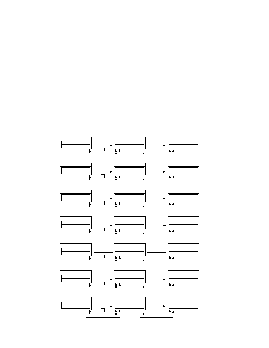
REV. A
AD73360
28
Programming a Single AD73360 for Data Mode Operation
This section describes a typical sequence in programming a
single AD73360 to operate in normal Data Mode. It details the
control (program) words that are sent to the device to configure
its internal registers and shows the typical output data received
during both Program and Data Modes. The device is connected
in Frame Sync Loop-Back Mode (see Figure 13), which forces
an input word from the DSP's Tx register each time the AD73360
outputs a word via the SDO/SDOFS lines (while the AD73360
is in Program Mode the data transmitted will be invalid ADC
data and will, in fact, be a modified version of the last control
word written in by the DSP). In each case the DSP's Tx register
is preloaded with the data before the frame pulse is received. In
Step 1, the part has just been reset and on the first output event
the AD73360 presents an invalid output word
1
. The DSP's Tx
register contains a control word that programs CRB with the
data byte 0x03. This sets the sample rate at 8 kHz (with a
APPENDIX A
master clock of 16.384 MHz). In Step 2, the control word in
the DSP's Tx register will cause all the AD73360s channels to
power up. This data is received by the AD73360 with the next
frame sync pulse. An invalid ADC word is also received at the
DSP's Rx register. Step 3 selects the settings for each channel
of the AD73360. This set can be repeated as necessary to pro-
gram all the channels to the desired settings. Steps 4 and 5
program the modes of each channel (i.e., single-ended or differ-
ential mode and normal or inverted). Step 6 puts the AD73360
into Data Mode and in Step 7 the first valid ADC word is
received.
NOTE
1
This sequence assumes that the DSP SPORT's Rx and Tx interrupts are
enabled. It is important to ensure there is no latency (separation) between
control words in a cascade configuration. This is especially the case when
programming Control Register B, as it contains settings for SCLK and
DMCLK rates.
DSP Tx REG
CONTROL WORD
1000 0001 0000 0011
DEVICE 1
ADC WORD 1*
0000 0000 0000 0000
DSP Rx REG
0000 0000 0000 0000
STEP 1
DON'T CARE
DSP Tx REG
CONTROL WORD
1000 0010 0000 0001
DEVICE 1
ADC WORD 1*
1011 1111 0000 0011
DSP Rx REG
1011 1111 0000 0011
STEP 2
DON'T CARE
DSP Tx REG
CONTROL WORD
1000 0011 1000 1111
DEVICE 1
ADC WORD 1*
1011 1010 0000 0001
DSP Rx REG
1011 1010 0000 0001
STEP 3
DON'T CARE
DSP Tx REG
CONTROL WORD
1000 0110 0011 1111
DEVICE 1
ADC WORD 1*
1011 1011 1000 1111
DSP Rx REG
1011 1011 1000 1111
STEP 4
DON'T CARE
DSP Tx REG
CONTROL WORD
1000 0111 0011 1111
DEVICE 1
ADC WORD 1*
1011 1111 0011 1111
DSP Rx REG
1011 1110 0011 1111
STEP 5
DON'T CARE
DSP Tx REG
CONTROL WORD
1000 0000 0000 0001
DEVICE 1
ADC WORD 1*
1011 1111 0011 1111
DSP Rx REG
1011 1111 0011 1111
STEP 6
DON'T CARE
DSP Tx REG
CONTROL WORD
0111 1111 1111 1111
DEVICE 1
ADC WORD 1
1000 0000 0000 0000
DSP Rx REG
1000 0000 0000 0000
STEP 7
ADC WORD 1
SET 8kHz SAMPLING
GLOBAL POWER-UP
SET CHANNEL GAINS
SET CHANNEL MODE
SET CHANNEL INVERSION
SET DATA MODE
RECEIVE VALID ADC DATA
*ADC DATA RECEIVED BY THE DSP DURING THE PROGRAMMING PHASE SHOULD NOT BE CONSIDERED VALID RESULTS
Figure 32. Programming a Single AD73360 for Operation in Data Mode
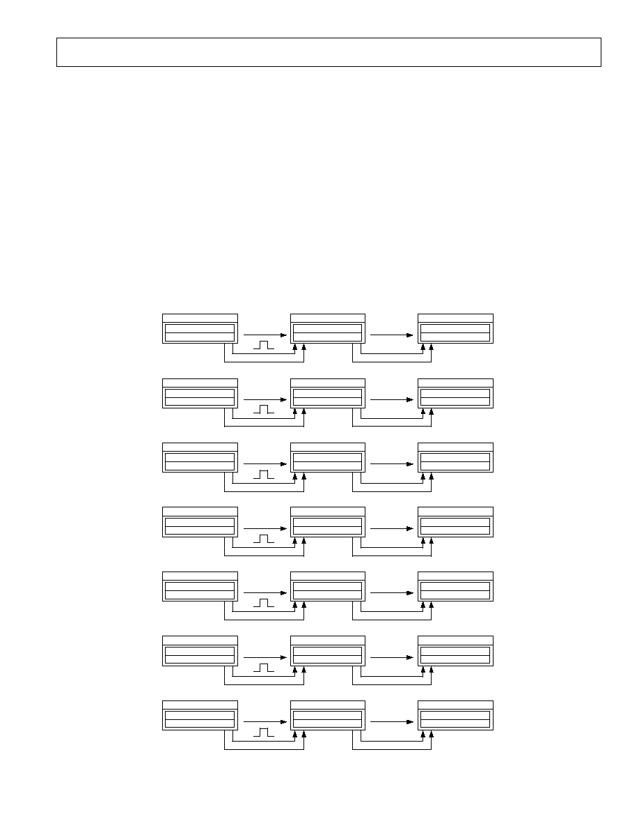
REV. A
AD73360
29
APPENDIX B
Programming a Single AD73360 for Mixed Mode Operation
This section describes a typical sequence in programming a
single AD73360 to operate in Mixed Mode. The device is con-
figured in Nonframe Sync Loop-Back (see Figure 14), which
allows the DSP's Tx Register to determine how many words are
sent to the device during one sample interval. In Nonframe
Sync Loop-Back mode care must be taken when writing to the
AD73360 that an ADC result or register read result contained
in the device's serial register is not corrupted by a write. The
best way to avoid this is to only write control words when the
AD73360 has no more data to send. This can limit the number
of times a DSP can write to the AD73360 and is dependant on
the SCLK speed and the number of channels powered up. In
this example it is assumed that there are only two channels
powered up and that there is adequate time to transmit data
after the ADC results have been read.
In Step 1, the device has just been reset and the on first output
event the AD73360 presents an invalid ADC sample word
1
.
Once this word has been received the DSP can begin transmit-
ting programming information to the AD73360. The first con-
trol word sets the sampling rate at 8 kHz. In Step 2, the DSP
instructs the AD73360 to power up channels 1 and 2 and sets
the gain of each. No data is read from the AD73360 at this
point. Steps 3 and 4 set the reference and places the part into
Mixed Mode. In Steps 5 and 6 valid ADC results are read from
the AD73360 and in Step 7 the DSP sends an instruction to the
AD73360 to change the gain of Channel 1.
NOTE
1
This sequence assumes that the DSP SPORT's Rx and Tx interrupts are
enabled. It is important to ensure there is no latency (separation) between
control words in a cascade configuration. This is especially the case when
programming Control Register B, as it contains settings for SCLK and
DMCLK rates.
DSP Tx REG
CONTROL WORD
1000 0001 0000 0011
DEVICE 1
ADC WORD 1*
0000 0000 0000 0000
DSP Rx REG
0000 0000 0000 0000
STEP 1
DON'T CARE
DSP Tx REG
CONTROL WORD
1000 0011 1111 1010
DEVICE 1
ADC WORD 1*
1011 1001 0000 0011
DSP Rx REG
0000 0000 0000 0000
STEP 2
DON'T CARE
DSP Tx REG
CONTROL WORD
1000 0010 1110 0000
DEVICE 1
ADC WORD 1*
1011 1011 1111 1010
DSP Rx REG
0000 0000 0000 0000
STEP 3
DON'T CARE
DSP Tx REG
CONTROL WORD
1000 0000 0000 0010
DEVICE 1
ADC WORD 1*
1011 1010 1110 0000
DSP Rx REG
0000 0000 0000 0000
STEP 4
DON'T CARE
DSP Tx REG
CONTROL WORD
0111 1111 1111 1111
DEVICE 1
ADC WORD 1
1000 0000 0000 0000
DSP Rx REG
1000 0000 0000 0000
STEP 5
ADC WORD 1
DSP Tx REG
CONTROL WORD
0111 1111 1111 1111
DEVICE 1
ADC WORD 2
1111 0000 0000 0000
DSP Rx REG
1111 0000 0000 0000
STEP 6
ADC WORD 2
DSP Tx REG
CONTROL WORD
1000 0011 1000 0010
DEVICE 1
INVALID DATA
xxxx xxxx xxxx xxxx
DSP Rx REG
1111 0000 0000 0000
STEP 7
ADC WORD 2
SET 8kHz SAMPLING
POWER UP CHANNEL 1&2 AND SET GAINS
POWER UP REFERENCE
SET MIXED MODE
CHANGE GAIN ON CHANNEL 1
RECEIVE VALID ADC DATA
RECEIVE VALID ADC DATA
*ADC DATA RECEIVED BY THE DSP DURING THE PROGRAMMING PHASE SHOULD NOT BE CONSIDERED VALID RESULTS
Figure 33. Programming a Single AD73360 for Operation in Mixed Mode

REV. A
AD73360
30
APPENDIX C
Configuring a Cascade of Two AD73360s to Operate in
Data Mode
This section describes a typical sequence of control words that
would be sent to a cascade of two AD73360s to set them up for
operation. It is not intended to be a definitive initialization
sequence, but will show users the typical input/output events
that occur in the programming and operation phases
1
. This
description panel refers to Figure 34.
In Step 1, we have the first output sample event following de-
vice reset. The SDOFS signal is raised on both devices simulta-
neously, which prepares the DSP Rx register to accept the ADC
word from Device 2, while SDOFS from Device 1 becomes an
SDIFS to Device 2. As the SDOFS of Device 2 is coupled to
the DSP's TFS and RFS, and to the SDIFS of Device 1, this
event also forces a new control word to be output from the DSP
Tx register to Device 1. The control word loaded to Device 1 is
addressed to Device 2 (i.e., the address field is 001). Device 1
will decrement the address field and pass it to Device 2 when
the next frame sync arrives. As the DSP is transmitting a control
word, Device 2 is outputting an invalid ADC word. (Note that
the AD73360 will not output valid ADC words until the device
is placed in either mixed mode or data mode. Any ADC values
received during the programming phase should be discarded.)
At the same time, Device 1 will output its ADC result to Device
2. Once all the data has been transferred, Device 1 will contain
an instruction for Device 2 (which instructs the part to set its
SCLK frequency), Device 2 will have received an ADC result
from Device 1 and the DSP will have received an ADC result
from Device 2.
In Step 2, Device 2 will begin transmitting the ADC word it
received from Device 1. This will cause the DSP to transmit a
second command word, which tells Device 1 to change its serial
clock. Simultaneously, Device 1 passes the first control word on
to Device 2. In this manner both devices receive control word
instructions and act upon them at the same time.
Step 3 is similar to Step 1 in that the DSP transmits a control
word for Device 2. Device 1 passes an invalid ADC result to
Device 2 and Device 2 transmits its own invalid ADC result to
the DSP.
In Step 4, Device 2 will transmit the invalid ADC sample it
received from Device 1 while receiving a control word from
Device 1 at the same time. Device 2 transmitting will cause the
DSP to transmit a control word for Device 1. This should be
similar to the control word transmitted in step 3 except that this
word is intended for Device 1. When transmission is complete
both devices have received instructions to power up all channels
and set the reference etc. Steps 3 and 4 can be repeated, as
necessary, to program other registers concerned with the analog
section.
Step N is the first stage of changing the operating modes of the
devices to Data Mode. As Device 2 outputs an ADC word the
DSP will transmit a control word intended for CRA of Device 2
to Device 1. As in Step 1, Device 1 will decrement the address
field and pass on the control word on the next frame sync.
In Step N + 1, Device 2 transmits an ADC word it received
from Device 1. This causes the DSP to transmit a control word
to Device 1 (intended for its CRA register). At the same time
Device 2 is receiving its control word from Device 1. Both de-
vices simultaneously receive commands to change from Program
Mode to Data Mode and the number of devices in the cascade is
also programmed here.
In Step N + 2, we begin to receive valid ADC data. Note that
the data comes from the last device in the chain (Device 2) first.
As Device 2 transmits its ADC data it is receiving ADC data
from Device 1. Any data transmitted from the DSP will be ig-
nored from now on.
In Step N + 3, Device 2 has received an ADC sample from
Device 1 and transmits it to the DSP. Steps N + 2 and N + 3
are repeated as long as samples are required.
NOTE
1
This sequence assumes that the DSP SPORT's Rx and Tx interrupts are
enabled. It is important to ensure that there is no latency (separation) between
control words in a cascade configuration. This is especially the case when
programming Control Register B as it contains settings for SCLK and DMCLK
rates.
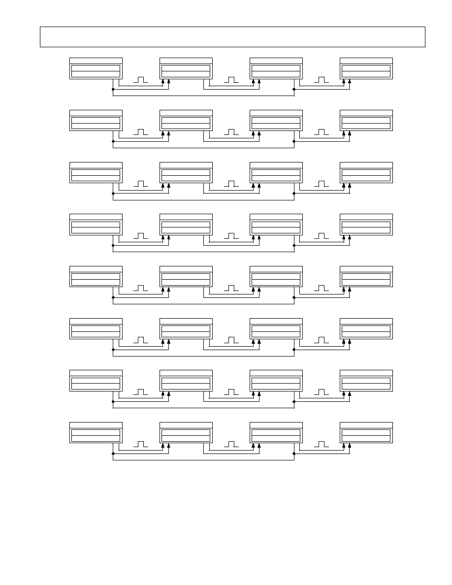
REV. A
AD73360
31
DSP Tx REG
CONTROL WORD 1
1000 1001 0000 0011
DEVICE 1
ADC WORD 1*
0000 0000 0000 0000
DEVICE 2
0000 0000 0000 0000
DSP Rx REG
ADC WORD 2*
STEP 1
ADC WORD 2*
0000 0000 0000 0000
DSP Tx REG
CONTROL WORD 1
1000 0001 0000 0011
DEVICE 1
ADC WORD 1*
xxxx xxxx xxxx xxxx
DEVICE 2
xxxx xxxx xxxx xxxx
DSP Rx REG
ADC WORD 1*
STEP 2
ADC WORD 2*
xxxx xxxx xxxx xxxx
DSP Tx REG
CONTROL WORD 2
1000 1010 1110 0001
DEVICE 1
ADC WORD 1*
xxxx xxxx xxxx xxxx
DEVICE 2
xxxx xxxx xxxx xxxx
DSP Rx REG
ADC WORD 2*
STEP 3
ADC WORD 2*
xxxx xxxx xxxx xxxx
DSP Tx REG
CONTROL WORD
1000 0010 1110 0001
DEVICE 1
ADC WORD 1*
xxxx xxxx xxxx xxxx
DEVICE 2
xxxx xxxx xxxx xxxx
DSP Rx REG
ADC WORD 1*
STEP 4
ADC WORD 2*
xxxx xxxx xxxx xxxx
DSP Tx REG
CONTROL WORD
1000 1000 0001 0001
DEVICE 1
ADC WORD 1*
xxxx xxxx xxxx xxxx
DEVICE 2
xxxx xxxx xxxx xxxx
DSP Rx REG
ADC WORD 2*
STEP N
ADC WORD 2*
xxxx xxxx xxxx xxxx
DSP Tx REG
CONTROL WORD
1000 0000 0001 0001
DEVICE 1
ADC WORD 1*
xxxx xxxx xxxx xxxx
DEVICE 2
xxxx xxxx xxxx xxxx
DSP Rx REG
ADC WORD 1*
STEP N+1
ADC WORD 2*
xxxx xxxx xxxx xxxx
DSP Tx REG
CONTROL WORD
0111 1111 1111 1111
DEVICE 1
ADC WORD 1
0000 0011 0101 1110
DEVICE 2
0000 0011 0101 1110
DSP Rx REG
ADC WORD 2
STEP N+2
ADC WORD 2*
0000 0011 0101 1110
DSP Tx REG
CONTROL WORD
0111 1111 1111 1111
DEVICE 1
ADC WORD 1
0011 1100 1111 1110
DEVICE 2
0000 0011 0101 1110
DSP Rx REG
ADC WORD 1
STEP N+3
ADC WORD 2
0000 0011 0101 1110
*ADC DATA RECEIVED BY THE DSP DURING THE PROGRAMMING PHASE SHOULD NOT BE CONSIDERED VALID RESULTS
Figure 34. Programming Two AD73360s in Cascade for Data Mode Operation

REV. A
AD73360
32
APPENDIX D
Configuring a Cascade of Two AD73360s to Operate in Mixed
Mode
This section describes a typical sequence of control words that
would be sent to a cascade of two AD73360s to configure them
for operation in Mixed Mode. It is not intended to be a defini-
tive initialization sequence, but will show users the typical input/
output events that occur in the programming and operation
phases
1
. This description panel refers to Figure 35.
In Step 1, we have the first output sample event following device
reset. The SDOFS signal is raised on both devices simulta-
neously, which prepares the DSP Rx register to accept the ADC
word from Device 2 while SDOFS from Device 1 becomes an
SDIFS to Device 2. The cascade is configured as nonFSLB,
which means that the DSP has control over what is transmitted
to the cascade. The DSP will receive an invalid ADC word from
Device 2 and simultaneously Device 2 is receiving an invalid
ADC word from Device 1. As both AD73360s are in Program
Mode there is only one output event per sample period. The
DSP can now send a control word to the AD73360s.
In Step 2, the DSP has finished transmitting the control word to
Device 1. Device 1 recognizes that this word is not intended for
it so it will decrement the address field and generate and SDOFS
and proceed to transmit the control word to the next device in
the chain. At this point the DSP should transmit a control word
for Device 1. This will ensure that both devices receive, and act
upon, the control words at the same time.
Step 3 shows completion of the first series of control word writes.
The DSP has now received an ADC word from Device 2 and
each device has received a control word that addresses Control
Register B and sets the SCLK and Sample Rate. When pro-
gramming a cascade of AD73360s in NonFSLB it is important
to ensure that control words which affect the operation of the
serial port are received by all devices simultaneously.
In Step 4, another sample interval has occurred and the
SDOFS on both devices are raised. Device 2 sends an ADC
result to the DSP and Device 1 sends an ADC result to Device
2. The remaining time before the next sample interval can be
used to program more registers in the AD73360s. Care must be
taken that the subsequent writes do not overlap the next sample
interval to avoid corrupting the data. The control words are
written as Device 2, Device 1, Device 2, etc.
Step 5 shows the DSP starting to program the ADC Control
Register to select channel gains, operating modes etc. In this
case the first write operation programs Control Register D to
power up ADC channels 1 and 2 with gains of 0 dBs. This step
can be repeated until all the registers have been programmed.
The devices should be programmed in the order Device 2,
Device 1, Device 2, etc.
In Step 6, the DSP transmits a control word for Device 2. This
control word set the Device count to 2 and instructs the AD73360
to go into Mixed Mode. When Device 1 receives this control
word it will decrement the address field and generate an SDOFS
to pass it on to Device 2.
In Step 7, the DSP transmits a control word for Device 1. This
should happen as Device 1 is transmitting the control word for
Device 2 to ensure that both device change into Mixed Mode at
the same time.
In Step 8, we begin receiving the first valid ADC words from
the cascade.
It is assumed that there is sufficient time to transmit all the
required Control Words in the allotted time.
NOTE
1
This sequence assumes that the DSP SPORT's Rx and Tx interrupts are
enabled. It is important to ensure there is no latency (separation) between
control words in a cascade configuration. This is especially the case when
programming Control Register B, as it contains settings for SCLK and
DMCLK rates.
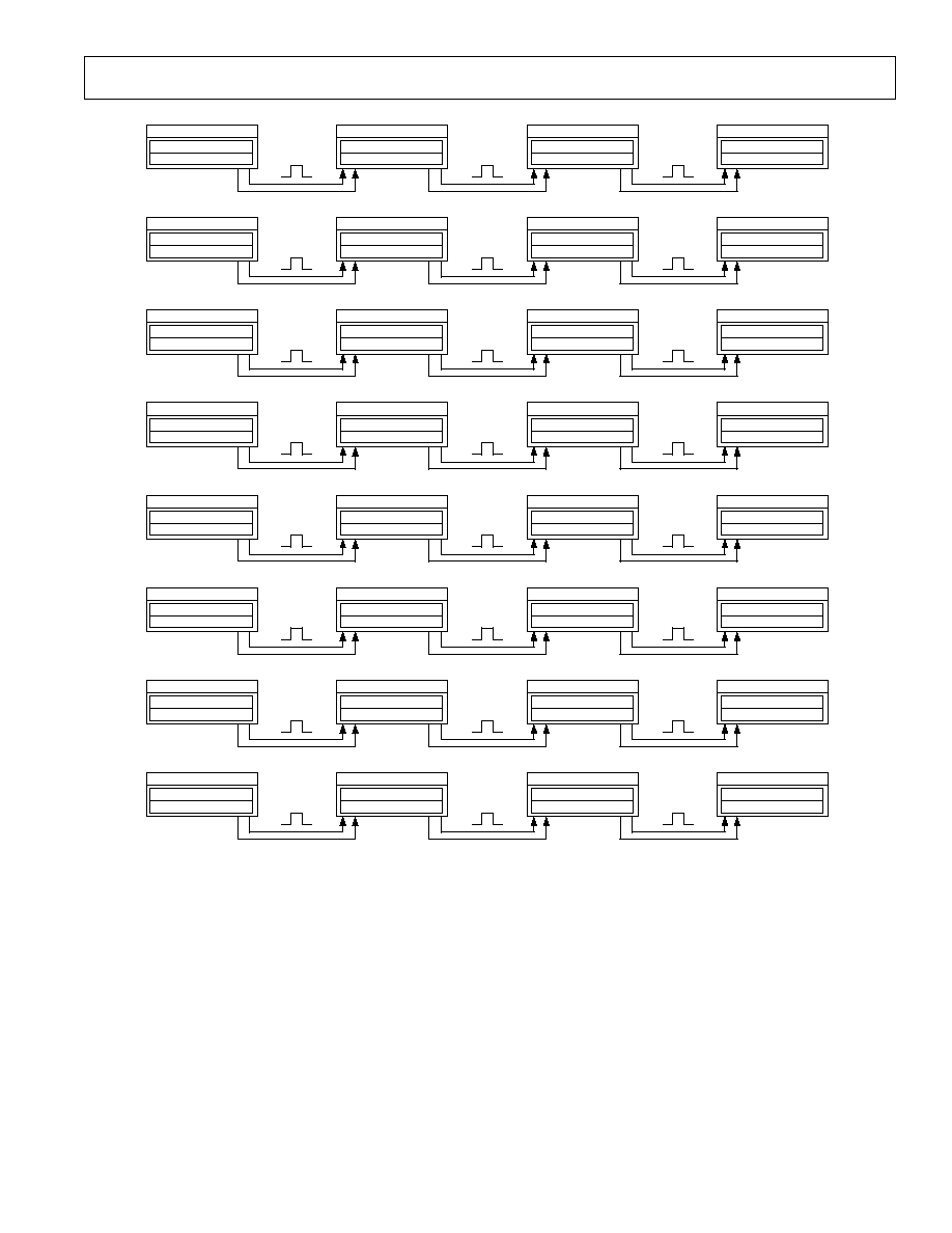
REV. A
AD73360
33
DSP Tx REG
CONTROL WORD 1
1000 1001 0000 0011
DEVICE 1
ADC WORD 1*
0000 0000 0000 0000
DEVICE 2
0000 0000 0000 0000
DSP Rx REG
DON'T CARE
STEP 1
ADC WORD 2*
xxxx xxxx xxxx xxxx
DSP Tx REG
CONTROL WORD 2
1000 0001 0001 0011
DEVICE 1
CONTROL WORD 1*
1000 1001 0001 0011
DEVICE 2
xxxx xxxx xxxx xxxx
DSP Rx REG
DON'T CARE
STEP 2
ADC WORD 2*
xxxx xxxx xxxx xxxx
DSP Tx REG
CONTROL WORD 2
1000 0001 0001 0011
DEVICE 1
ADC WORD 1*
1000 1001 0001 0011
DEVICE 2
1000 1001 0001 0011
DSP Rx REG
DON'T CARE
STEP 3
ADC WORD 2*
xxxx xxxx xxxx xxxx
DSP Tx REG
CONTROL WORD
1000 0010 1110 0001
DEVICE 1
ADC WORD 1*
xxxx xxxx xxxx xxxx
DEVICE 2
xxxx xxxx xxxx xxxx
DSP Rx REG
DON'T CARE
STEP 4
ADC WORD 2*
xxxx xxxx xxxx xxxx
DSP Tx REG
CONTROL WORD
1000 1011 1000 1000
DEVICE 1
ADC WORD 1*
1000 1011 1000 1000
DEVICE 2
xxxx xxxx xxxx xxxx
DSP Rx REG
DON'T CARE
STEP 5
ADC WORD 2*
xxxx xxxx xxxx xxxx
DSP Tx REG
CONTROL WORD
1000 1000 0001 0011
DEVICE 1
ADC WORD 1*
1000 1000 0001 0011
DEVICE 2
xxxx xxxx xxxx xxxx
DSP Rx REG
DON'T CARE
STEP 6
ADC WORD 2*
xxxx xxxx xxxx xxxx
DSP Tx REG
CONTROL WORD 1
1000 0000 0001 0011
DEVICE 1
ADC WORD 1**
1000 1001 0001 0011
DEVICE 2
1000 0000 0001 0011
DSP Rx REG
ADC WORD 2
STEP 7
ADC WORD 2*
0000 0011 0101 1110
DSP Tx REG
CONTROL WORD 1
0111 1111 1111 1111
DEVICE 1
ADC WORD 1
0011 1100 1111 1110
DEVICE 2
0000 0011 0101 1110
DSP Rx REG
ADC WORD 2
STEP 8
ADC WORD 2
0000 0011 0101 1110
*ADC DATA RECEIVED BY THE DSP DURING THE PROGRAMMING PHASE SHOULD NOT BE CONSIDERED VALID RESULTS.
**THIS CONTROL WORD IS NOT INTENDED FOR THE DEVICE THAT HAS RECEIVED IT. ITS ADDRESS FIELD WILL BE DECREMENTED
AND THE DATA WILL BE TRANSMITTED TO THE NEXT DEVICE IN THE CASCADE.
Figure 35. Programming Two AD73360s in Cascade for Mixed Mode

REV. A
AD73360
34
TABLE OF CONTENTS
Topic
Page
FEATURES . . . . . . . . . . . . . . . . . . . . . . . . . . . . . . . . . . . . . 1
FUNCTIONAL BLOCK DIAGRAM . . . . . . . . . . . . . . . . . 1
GENERAL DESCRIPTION . . . . . . . . . . . . . . . . . . . . . . . . . 1
SPECIFICATIONS (3 V) . . . . . . . . . . . . . . . . . . . . . . . . . . . 2
SPECIFICATIONS (5 V) . . . . . . . . . . . . . . . . . . . . . . . . . . . 4
TIMING CHARACTERISTICS (3 V) . . . . . . . . . . . . . . . . . 6
TIMING CHARACTERISTICS (5 V) . . . . . . . . . . . . . . . . . 6
Timing Diagrams . . . . . . . . . . . . . . . . . . . . . . . . . . . . . . . . 7
Performance Graphs . . . . . . . . . . . . . . . . . . . . . . . . . . . . . 7
ABSOLUTE MAXIMUM RATINGS . . . . . . . . . . . . . . . . . 8
ORDERING GUIDE . . . . . . . . . . . . . . . . . . . . . . . . . . . . . . 8
PIN CONFIGURATIONS . . . . . . . . . . . . . . . . . . . . . . . . . . 8
PIN FUNCTION DESCRIPTION . . . . . . . . . . . . . . . . . . . 9
TERMINOLOGY . . . . . . . . . . . . . . . . . . . . . . . . . . . . . . . . 10
ABBREVIATIONS . . . . . . . . . . . . . . . . . . . . . . . . . . . . . . . 10
FUNCTIONAL DESCRIPTION . . . . . . . . . . . . . . . . . . . . 11
General Description . . . . . . . . . . . . . . . . . . . . . . . . . . . . . 11
Encoder Channel . . . . . . . . . . . . . . . . . . . . . . . . . . . . . . . 11
Signal Conditioner . . . . . . . . . . . . . . . . . . . . . . . . . . . . . . 11
Programmable Gain Amplifier . . . . . . . . . . . . . . . . . . . . . 11
ADC . . . . . . . . . . . . . . . . . . . . . . . . . . . . . . . . . . . . . . . . 11
Analog Sigma-Delta Modulator . . . . . . . . . . . . . . . . . . . . 11
Decimation Filter . . . . . . . . . . . . . . . . . . . . . . . . . . . . . . . 12
ADC Coding . . . . . . . . . . . . . . . . . . . . . . . . . . . . . . . . . . 12
Voltage Reference . . . . . . . . . . . . . . . . . . . . . . . . . . . . . . 12
Serial Port (SPORT) . . . . . . . . . . . . . . . . . . . . . . . . . . . . 13
SPORT Overview . . . . . . . . . . . . . . . . . . . . . . . . . . . . . . . 13
SPORT Register Maps . . . . . . . . . . . . . . . . . . . . . . . . . . . 14
Control Register Tables . . . . . . . . . . . . . . . . . . . . . . . . . . 14
REGISTER BIT DESCRIPTIONS . . . . . . . . . . . . . . . . . . 17
Master Clock Divider . . . . . . . . . . . . . . . . . . . . . . . . . . . . 19
Serial Clock Rate Divider . . . . . . . . . . . . . . . . . . . . . . . . . 19
Decimation Rate Divider . . . . . . . . . . . . . . . . . . . . . . . . . 19
Topic
Page
OPERATION . . . . . . . . . . . . . . . . . . . . . . . . . . . . . . . . . . . 19
General Description . . . . . . . . . . . . . . . . . . . . . . . . . . . . 19
Resetting the AD73360 . . . . . . . . . . . . . . . . . . . . . . . . . . 20
Power Management . . . . . . . . . . . . . . . . . . . . . . . . . . . . . 20
Operating Modes . . . . . . . . . . . . . . . . . . . . . . . . . . . . . . . 20
Program (Control) Mode . . . . . . . . . . . . . . . . . . . . . . . . . 20
Data Mode . . . . . . . . . . . . . . . . . . . . . . . . . . . . . . . . . . . . 20
Mixed Program/Data Mode . . . . . . . . . . . . . . . . . . . . . . . 20
INTERFACING . . . . . . . . . . . . . . . . . . . . . . . . . . . . . . . . . 21
Digital Interfacing . . . . . . . . . . . . . . . . . . . . . . . . . . . . . . 21
Cascade Operation . . . . . . . . . . . . . . . . . . . . . . . . . . . . . . 23
PERFORMANCE . . . . . . . . . . . . . . . . . . . . . . . . . . . . . . . . 24
Encoder Section . . . . . . . . . . . . . . . . . . . . . . . . . . . . . . . . 24
Encoder Group Delay . . . . . . . . . . . . . . . . . . . . . . . . . . . 25
DESIGN CONSIDERATIONS . . . . . . . . . . . . . . . . . . . . . 25
Analog Inputs . . . . . . . . . . . . . . . . . . . . . . . . . . . . . . . . . . 25
Digital Interface . . . . . . . . . . . . . . . . . . . . . . . . . . . . . . . . 26
Grounding and Layout . . . . . . . . . . . . . . . . . . . . . . . . . . . 26
DSP Programming Considerations . . . . . . . . . . . . . . . . . 26
DSP SPORT Configuration . . . . . . . . . . . . . . . . . . . . . . . 26
DSP SPORT Interrupts . . . . . . . . . . . . . . . . . . . . . . . . . . 27
APPLICATION EXAMPLES . . . . . . . . . . . . . . . . . . . . . . . 27
Vector Motor Control . . . . . . . . . . . . . . . . . . . . . . . . . . . 27
Industrial Power Metering . . . . . . . . . . . . . . . . . . . . . . . . 27
APPENDIX A (Single Device Data Mode Operation) . . . . 28
APPENDIX B (Single Device Mixed Mode Operation) . . . . . 29
APPENDIX C (Two Devices in Data Mode Operation) . . . . 30
APPENDIX D (Two Devices in Mixed Mode Operation) . . . 32
OUTLINE DIMENSIONS . . . . . . . . . . . . . . . . . . . . . . . . . 35
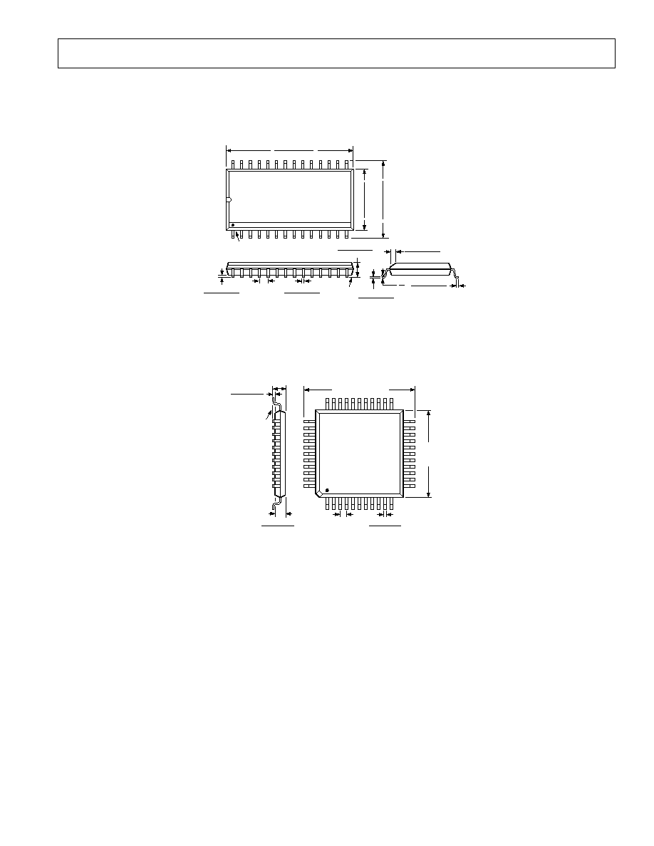
REV. A
AD73360
35
OUTLINE DIMENSIONS
Dimensions shown in inches and (mm).
28-Lead Small Outline IC
(R-28)
SEATING
PLANE
0.0118 (0.30)
0.0040 (0.10)
0.0192 (0.49)
0.0138 (0.35)
0.1043 (2.65)
0.0926 (2.35)
0.0500
(1.27)
BSC
0.0125 (0.32)
0.0091 (0.23)
0.0500 (1.27)
0.0157 (0.40)
8
0
0.0291 (0.74)
0.0098 (0.25)
45
0.7125 (18.10)
0.6969 (17.70)
0.4193 (10.65)
0.3937 (10.00)
0.2992 (7.60)
0.2914 (7.40)
PIN 1
28
15
14
1
44-Lead Thin Quad Flatpack
(SU-44)
TOP VIEW
(PINS DOWN)
1
33
34
44
11
12
23
22
0.018 (0.45)
0.012 (0.30)
0.031 (0.80)
BSC
0.394
(10.0)
SQ
0.472 (12.00) SQ
0.041 (1.05)
0.037 (0.95)
SEATING
PLANE
0.047 (1.20)
MAX
0.006 (0.15)
0.002 (0.05)
C3594
0
3/00 (rev. A)
PRINTED IN U.S.A.