Äîêóìåíòàöèÿ è îïèñàíèÿ www.docs.chipfind.ru
REV. B
Information furnished by Analog Devices is believed to be accurate and
reliable. However, no responsibility is assumed by Analog Devices for its
use, nor for any infringements of patents or other rights of third parties
which may result from its use. No license is granted by implication or
otherwise under any patent or patent rights of Analog Devices.
a
AD73311
One Technology Way, P.O. Box 9106, Norwood, MA 02062-9106, U.S.A.
Tel: 781/329-4700
World Wide Web Site: http://www.analog.com
Fax: 781/326-8703
© Analog Devices, Inc., 2000
Low Cost, Low Power CMOS
General Purpose Analog Front End
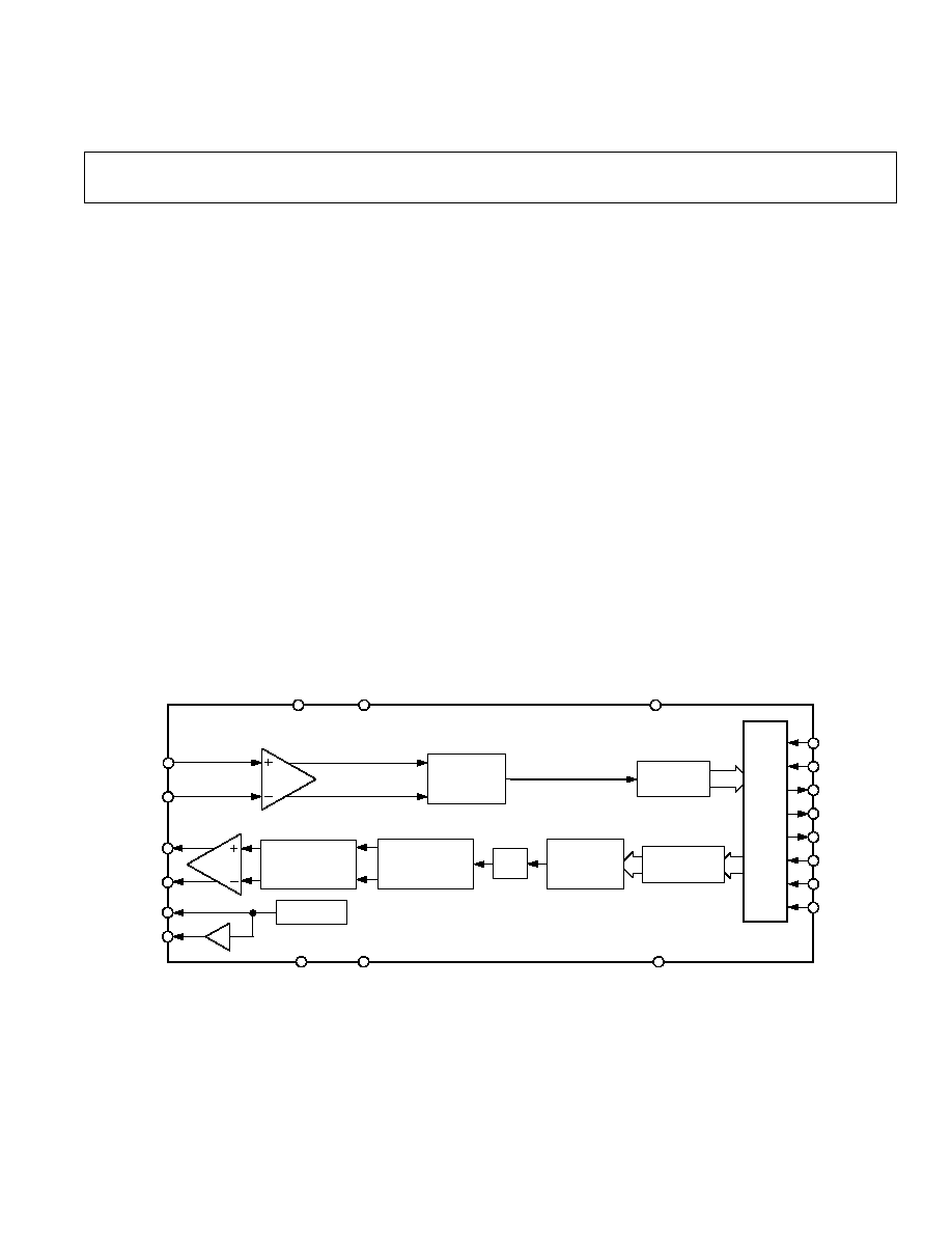
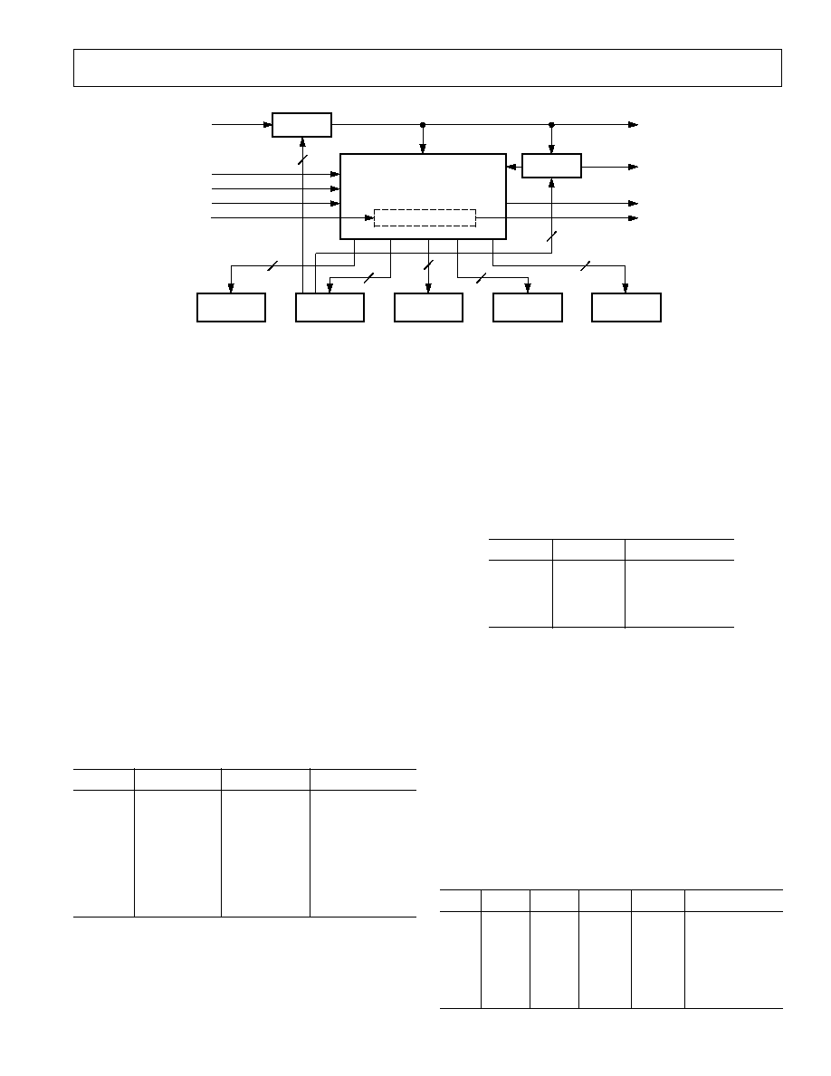
FUNCTIONAL BLOCK DIAGRAM
AD73311
AGND1
AGND2
DGND
DVDD
AVDD2
AVDD1
VINP
VINN
VOUTP
VOUTN
REFCAP
REFOUT
SDI
SDIFS
SCLK
SDO
SDOFS
SE
MCLK
RESET
1-BIT
DAC
REFERENCE
SERIAL
I/O
PORT
INTERPOLATOR
DECIMATOR
SWITCHED-
CAPACITOR
LOW-PASS FILTER
CONTINUOUS
TIME
LOW-PASS FILTER
+6/15dB
PGA
0/38dB
PGA
ANALOG
SIGMA-DELTA
MODULATOR
DIGITAL
SIGMA-DELTA
MODULATOR
FEATURES
16-Bit A/D Converter
16-Bit D/A Converter
Programmable Input/Output Sample Rates
75 dB ADC SNR
70 dB DAC SNR
64 kS/s Maximum Sample Rate
90 dB Crosstalk
Low Group Delay (25
s Typ per ADC Channel,
50 s Typ per DAC Channel)
Programmable Input/Output Gain
Flexible Serial Port which Allows up to 8 Devices
to Be Connected in Cascade
Single (+2.7 V to +5.5 V) Supply Operation
50 mW Max Power Consumption at 2.7 V
On-Chip Reference
20-Lead SOIC/SSOP Package
APPLICATIONS
General Purpose Analog I/O
Speech Processing
Cordless and Personal Communications
Telephony
Active Control of Sound & Vibration
Data Communications
GENERAL DESCRIPTION
The AD73311 is a complete front-end processor for general
purpose applications including speech and telephony. It features
a 16-bit A/D conversion channel and a 16-bit D/A conversion
channel. Each channel provides 70 dB signal-to-noise ratio over
a voiceband signal bandwidth. The final channel bandwidth can
be reduced, and signal-to-noise ratio improved, by external
digital filtering in a DSP engine.
The AD73311 is suitable for a variety of applications in the
speech and telephony area including low bit rate, high quality
compression, speech enhancement, recognition and synthesis.
The low group delay characteristic of the part makes it suitable
for single or multichannel active control applications.
The gains of the A/D and D/A conversion channels are pro-
grammable over 38 dB and 21 dB ranges respectively. An
on-chip reference voltage is included to allow single supply
operation. A serial port (SPORT) allows easy interfacing of
single or cascaded devices to industry standard DSP engines.
The AD73311 is available in both 20-lead SOIC and SSOP
packages.

2
REV. B
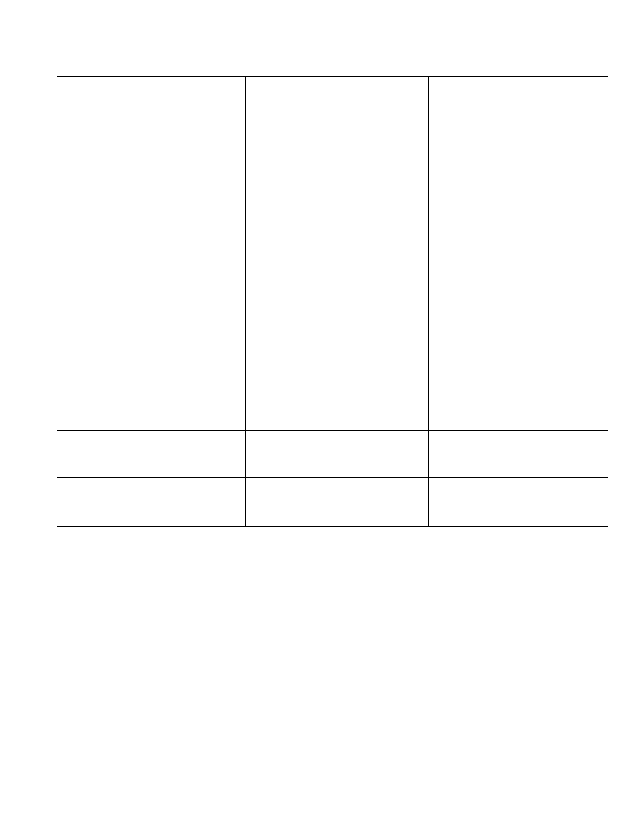
AD73311SPECIFICATIONS
1
AD73311A
Parameter
Min
Typ
Max
Unit
Test Conditions/Comments
REFERENCE
5VEN = 0
REFCAP
Absolute Voltage, V
REFCAP
1.08
1.2
1.32
V
REFCAP TC
50
ppm/
°C
0.1
µF Capacitor Required from
REFOUT
REFCAP to AGND2
Typical Output Impedance
68
Absolute Voltage, V
REFOUT
1.08
1.2
1.32
V
Unloaded
Minimum Load Resistance
1
k
Maximum Load Capacitance
100
pF
ADC SPECIFICATIONS
Maximum Input Range at VIN
2, 3
1.578
V p-p
5VEN = 0, Measured Differentially
2.85
dBm
Nominal Reference Level at VIN
1.0954
V p-p
5VEN = 0, Measured Differentially
(0 dBm0)
6.02
dBm
Absolute Gain
PGA = 0 dB
0.75
0.1
+1.0
dB
1.0 kHz, 0 dBm0
PGA = 38 dB
1.5
0.5
+0.5
dB
1.0 kHz, 0 dBm0
Gain Tracking Error
±0.1
dB
1.0 kHz, +3 dBm0 to 50 dBm0
Signal to (Noise + Distortion)
Refer to Figure 5
PGA = 0 dB
70
76
dB
300 Hz to 3.4 kHz Frequency Range
55
56
dB
0 Hz to 32 kHz Frequency Range
PGA = 38 dB
61
65
dB
300 Hz to 3.4 kHz Frequency Range
53
54
dB
0 Hz to 32 kHz Frequency Range
Total Harmonic Distortion
PGA = 0 dB
83
70
dB
PGA = 38 dB
83
70
dB
Intermodulation Distortion
78
dB
PGA = 0 dB
Idle Channel Noise
76
dBm0
PGA = 0 dB
Crosstalk
100
dB
ADC Input Signal Level: 1.0 kHz, 0 dBm0
DAC Input at Idle
DC Offset
20
+15
+50
mV
PGA = 0 dB
Power Supply Rejection
55
dB
Input Signal Level at AVDD and DVDD
Pins 1.0 kHz, 100 mV p-p Sine Wave
Group Delay
4, 5
25
µs
64 kHz Output Sample Rate
Input Resistance at VIN
2, 4
25
k
6
DMCLK = 16.384 MHz
DAC SPECIFICATIONS
Maximum Voltage Output Swing
2
Single Ended
1.578
V p-p
5VEN = 0, PGA = 6 dB
2.85
dBm
Differential
3.156
V p-p
5VEN = 0, PGA = 6 dB
3.17
dBm
Nominal Voltage Output Swing (0 dBm0)
Single-Ended
1.0954
V p-p
5VEN = 0, PGA = 6 dB
6.02
dBm
Differential
2.1909
V p-p
5VEN = 0, PGA = 6 dB
0
dBm
Output Bias Voltage
1.08
1.2
1.32
V
5VEN = 0, REFOUT Unloaded
Absolute Gain
0.75
+0.2
+1.0
dB
1.0 kHz, 0 dBm0
Gain Tracking Error
±0.1
dB
1.0 kHz, +3 dBm0 to 50 dBm0
Signal to (Noise + Distortion)
AVDD = +3 V
± 5%; Refer to Figure 5
PGA = 0 dB
62.5
70
dB
300 Hz to 3.4 kHz Frequency Range
62.5
dB
0 Hz to 32 kHz Frequency Range
PGA = 6 dB
62.5
71
dB
300 Hz to 3.4 kHz Frequency Range
62.5
dB
0 Hz to 32 kHz Frequency Range
Total Harmonic Distortion
AVDD = +3 V
± 5%
PGA = 0 dB
70
62.5
dB
PGA = 6 dB
70
62.5
dB
Intermodulation Distortion
68
dB
PGA = 0 dB
Idle Channel Noise
82
dBm0
PGA = 0 dB
Crosstalk
100
dB
ADC Input Signal Level: AGND; DAC
Output Signal Level: 1.0 kHz, 0 dBm0
(AVDD = +3 V 10%; DVDD = +3 V 10%; DGND = AGND = 0 V, f
MCLK
= 16.384 MHz,
F
S
= 64 kHz; T
A
= T
MIN
to T
MAX
, unless otherwise noted)

AD73311A
Parameter
Min
Typ
Max
Unit
Test Conditions/Comments
DAC SPECIFICATIONS (Continued)
Power Supply Rejection
55
dB
Input Signal Level at AVDD and DVDD
Pins: 1.0 kHz, 100 mV p-p Sine Wave
Group Delay
4, 5
25
µs
64 kHz Input Sample Rate, Interpolator
Bypassed (CRE:5 = 1)
Output DC Offset
2, 7
30
+20
+70
mV
PGA = 6 dB
Minimum Load Resistance, R
L
2, 8
Single-Ended
150
Differential
150
Maximum Load Capacitance, C
L
2, 8
Single-Ended
500
pF
Differential
100
pF
FREQUENCY RESPONSE
(ADC AND DAC)
9
Typical Output
0 Hz
0
dB
2000 Hz
0.1
dB
4000 Hz
0.25
dB
8000 Hz
0.6
dB
12000 Hz
1.4
dB
16000 Hz
2.8
dB
20000 Hz
4.5
dB
Channel Frequency Response Is
24000 Hz
7.0
dB
Programmable by Means of External
28000 Hz
9.5
dB
Digital Filtering
> 32000 Hz
< 12.5
dB
LOGIC INPUTS
V
INH
, Input High Voltage
V
DD
0.8
V
DD
V
V
INL
, Input Low Voltage
0
0.8
V
I
IH
, Input Current
10
µA
C
IN
, Input Capacitance
10
pF
LOGIC OUTPUT
V
OH
, Output High Voltage
V
DD
0.4
V
DD
V
|IOUT|
100 µA
V
OL
, Output Low Voltage
0
0.4
V
|IOUT|
100 µA
Three-State Leakage Current
10
+10
µA
POWER SUPPLIES
AVDD1, AVDD2
2.7
3.3
V
DVDD
2.7
3.3
V
I
DD
10
See Table I
NOTES
1
Operating temperature range is as follows: 40
°C to +85°C. Therefore, T
MIN
= 40
°C and T
MAX
= +85
°C.
2
Test conditions: Input PGA set for 0 dB gain, Output PGA set for 6 dB gain, no load on analog outputs (unless otherwise noted).
3
At input to sigma-delta modulator of ADC.
4
Guaranteed by design.
5
Overall group delay will be affected by the sample rate and the external digital filtering.
6
The ADC's input impedance is inversely proportional to DMCLK and is approximated by: (4
× 10
11
)/DMCLK.
7
Between VOUTP and VOUTN.
8
At VOUT output.
9
Frequency responses of ADC and DAC measured with input at audio reference level (the input level that produces an output level of 10 dBm0), with 38 dB preamplifier
bypassed and input gain of 0 dB.
10
Test Conditions: no load on digital inputs, analog inputs ac coupled to ground, no load on analog outputs.
Specifications subject to change without notice.
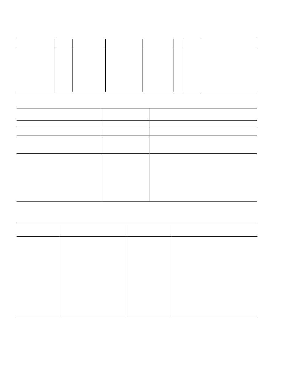
Table I. Current Summary (AVDD = DVDD = +3.3 V)
Analog
Internal Digital
External Interface
Total Current
MCLK
Conditions
Current Current
Current
(Max)
SE
ON
Comments
ADC On Only
7
3
0.5
11.5
1
YES
REFOUT Disabled
ADC and DAC On
10
5
0.5
17.5
1
YES
REFOUT Disabled
REFCAP On Only
0.75
0
0
1.2
0
NO
REFOUT Disabled
REFCAP and
REFOUT On Only 3.0
0
0
4.5
0
NO
All Sections Off
0
0.85
0
1.2
0
YES
MCLK Active Levels Equal to
0 V and DVDD
All Sections Off
0.00
0.007
0
0.04
0
NO
Digital Inputs Static and Equal
to 0 V or DVDD
The above values are in mA and are typical values unless otherwise noted.
AD73311
3
REV. B

(AVDD = +5 V 10%; DVDD = +5 V 10%; DGND = AGND = 0 V, f
MCLK
= 16.384 MHz,
F
S
= 64 kHz; T
A
= T
MIN
to T
MAX
, unless otherwise noted)
AD73311A
Parameter
Min
Typ
Max
Unit
Test Conditions/Comments
REFERENCE
REFCAP
Absolute Voltage, V
REFCAP
1.2
V
5VEN = 0
2.4
V
5VEN = 1
REFCAP TC
50
ppm/
°C 0.1 µF Capacitor Required from
REFOUT
REFCAP to AGND2
Typical Output Impedance
68
Absolute Voltage, V
REFOUT
1.2
V
5VEN = 0, Unloaded
2.4
V
5VEN = 1, Unloaded
Minimum Load Resistance
2
k
5VEN = 1
Maximum Load Capacitance
100
pF
ADC SPECIFICATIONS
Maximum Input Range at VIN
2, 3
3.156
V p-p
5VEN = 1, Measured Differentially
3.17
dBm
Nominal Reference Level at VIN
2.1908
V p-p
5VEN = 1, Measured Differentially
(0 dBm0)
0
dBm
Absolute Gain
PGA = 0 dB
0.1
dB
1.0 kHz, 0 dBm0
PGA = 38 dB
0.5
dB
1.0 kHz, 0 dBm0
Gain Tracking Error
±0.1
dB
1.0 kHz, +3 dBm0 to 50 dBm0
Signal to (Noise + Distortion)
Refer to Figure 5
PGA = 0 dB
76
dB
300 Hz to 3.4 kHz Frequency Range
59
dB
0 Hz to 32 kHz Frequency Range
PGA = 38 dB
71
dB
300 Hz to 3.4 kHz Frequency Range
57
dB
0 Hz to 32 kHz Frequency Range
Total Harmonic Distortion
PGA = 0 dB
76
dB
PGA = 38 dB
69
dB
Intermodulation Distortion
69
dB
PGA = 0 dB
Idle Channel Noise
67
dBm0
PGA = 0 dB
Crosstalk
80
dB
ADC Input Signal Level: 1.0 kHz, 0 dBm0
DAC Input at Idle
DC Offset
+20
mV
PGA = 0 dB
Power Supply Rejection
55
dB
Input Signal Level at AVDD and DVDD
Pins 1.0 kHz, 100 mV p-p Sine Wave
Group Delay
4, 5
25
µs
64 kHz Output Sample Rate
Input Resistance at VIN
2, 4
25
k
6
DMCLK = 16.384 MHz
DAC SPECIFICATIONS
Maximum Voltage Output Swing
2
Single Ended
3.156
V p-p
5VEN = 1, PGA = 6 dB
3.17
dBm
Differential
6.312
V p-p
5VEN = 1, PGA = 6 dB
9.19
dBm
Nominal Voltage Output Swing (0 dBm0)
Single-Ended
2.1908
V p-p
5VEN = 1, PGA = 6 dB
0
dBm
Differential
4.3918
V p-p
5VEN = 1, PGA = 6 dB
6.02
dBm
Output Bias Voltage
V
REFOUT
V typ
5VEN = 1, REFOUT Unloaded
Absolute Gain
±0.4
dB
1.0 kHz, 0 dBm0
Gain Tracking Error
±0.1
dB
1.0 kHz, +3 dBm0 to 50 dBm0
Signal to (Noise + Distortion)
Refer to Figure 5
PGA = 0 dB
66
dB
300 Hz to 3.4 kHz Frequency Range
64
dB
0 Hz to 32 kHz Frequency Range
PGA = 6 dB
66
dB
300 Hz to 3.4 kHz Frequency Range
64
dB
0 Hz to 32 kHz Frequency Range
Total Harmonic Distortion
PGA = 0 dB
62.5
dB
PGA = 6 dB
62.5
dB
Intermodulation Distortion
60
dB
PGA = 0
Idle Channel Noise
75
dBm0
PGA = 0
Crosstalk
80
dB
ADC Input Signal Level: AGND; DAC
Output Signal Level: 1.0 kHz, 0 dBm0
AD73311SPECIFICATIONS
1
4
REV. B
5
REV. B
AD73311
AD73311A
Parameter
Min
Typ
Max
Unit
Test Conditions/Comments
DAC SPECIFICATIONS (Continued)
Power Supply Rejection
55
dB
Input Signal Level at AVDD and DVDD
Pins: 1.0 kHz, 100 mV p-p Sine Wave
Group Delay
4, 5
25
µs
64 kHz Input Sample Rate, Interpolator
Bypassed (CRE:5 = 1)
Output DC Offset
2, 7
+30
mV
PGA = 6 dB
Minimum Load Resistance, R
L
2, 8
Single-Ended
150
Differential
150
Maximum Load Capacitance, C
L
2, 8
Single-Ended
500
pF
Differential
100
pF
FREQUENCY RESPONSE
(ADC AND DAC)
9
Typical Output
0 Hz
0
dB
2000 Hz
0.1
dB
4000 Hz
0.25
dB
8000 Hz
0.6
dB
12000 Hz
1.4
dB
16000 Hz
2.8
dB
20000 Hz
4.5
dB
Channel Frequency Response Is
24000 Hz
7.0
dB
Programmable by Means of External
28000 Hz
9.5
dB
Digital Filtering
> 32000 Hz
< 12.5
dB
LOGIC INPUTS
V
INH
, Input High Voltage
V
DD
0.8
V
DD
V
V
INL
, Input Low Voltage
0
0.8
V
I
IH
, Input Current
0.5
µA
C
IN
, Input Capacitance
10
pF
LOGIC OUTPUT
V
OH
, Output High Voltage
V
DD
0.4
V
DD
V
|I
OUT
| < 100
µA
V
OL
, Output Low Voltage
0
0.4
V
|I
OUT
| < 100
µA
Three-State Leakage Current
0.3
µA
POWER SUPPLIES
AVDD1, AVDD2
4.5
5.5
V
DVDD
4.5
5.5
V
I
DD
10
See Table II
N
OTES
1
Operating temperature range is as follows: 40
°C to +85°C. Therefore, T
MIN
= 40
°C and T
MAX
= +85
°C.
2
Test conditions: Input PGA set for 0 dB gain, Output PGA set for 6 dB gain, no load on analog outputs (unless otherwise stated).
3
At input to sigma-delta modulator of ADC.
4
Guaranteed by design.
5
Overall group delay will be affected by the sample rate and the external digital filtering.
6
The ADC's input impedance is inversely proportional to DMCLK and is approximated by: (4
× 10
11
)/DMCLK.
7
Between VOUTP and VOUTN.
8
At VOUT output.
9
Frequency responses of ADC and DAC measured with input at audio reference level (the input level that produces an output level of 10 dBm0), with 38 dB preamplifier
bypassed and input gain of 0 dB.
10
Test conditions: no load on digital inputs, analog inputs ac coupled to ground, no load on analog outputs.
Specifications subject to change without notice.
AD73311
6
REV. B
Table III. Signal Ranges
3 V Power Supply
5 V Power Supply
5VEN = 0
5VEN = 0
5VEN = 1
V
REFCAP
1.2 V
± 10%
1.2 V
2.4 V
V
REFOUT
1.2 V
± 10%
1.2 V
2.4 V
ADC
Maximum Input Range
at V
IN
1.578 V p-p
1.578 V p-p
3.156 V p-p
Nominal Reference Level
1.0954 V p-p
1.0954 V p-p
2.1908 V p-p
DAC
Maximum Voltage
Output Swing
Single-Ended
1.578 V p-p
1.578 V p-p
3.156 V p-p
Differential
3.156 V p-p
3.156 V p-p
6.312 V p-p
Nominal Voltage
Output Swing
Single-Ended
1.0954 V p-p
1.0954 V p-p
2.1908 V p-p
Differential
2.1909 V p-p
2.1909 V p-p
4.3818 V p-p
Output Bias Voltage
V
REFOUT
V
REFOUT
V
REFOUT
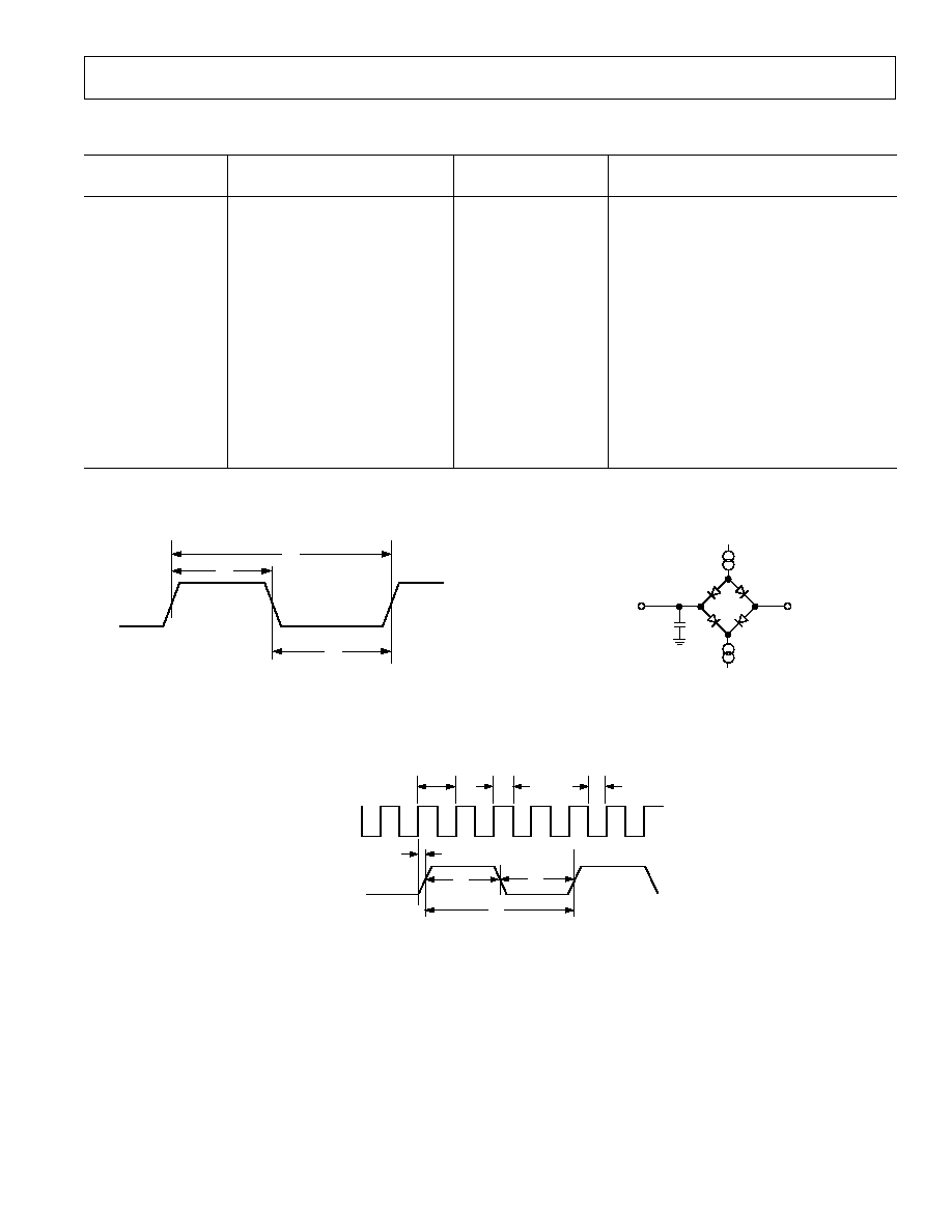
TIMING CHARACTERISTICS
Limit at
Parameter
T
A
= 40 C to +85 C
Unit
Description
Clock Signals
See Figure 1
t
1
61
ns min
MCLK Period
t
2
24.4
ns min
MCLK Width High
t
3
24.4
ns min
MCLK Width Low
Serial Port
See Figures 3 and 4
t
4
t
1
ns min
SCLK Period
t
5
0.4
× t
1
ns min
SCLK Width High
t
6
0.4
× t
1
ns min
SCLK Width Low
t
7
20
ns min
SDI/SDIFS Setup Before SCLK Low
t
8
0
ns min
SDI/SDIFS Hold After SCLK Low
t
9
10
ns max
SDOFS Delay from SCLK High
t
10
10
ns min
SDOFS Hold After SCLK High
t
11
10
ns min
SDO Hold After SCLK High
t
12
10
ns max
SDO Delay from SCLK High
t
13
30
ns max
SCLK Delay from MCLK
(AVDD = +3 V 10%; DVDD = +3 V 10%; AGND = DGND = 0 V; T
A
= T
MlN
to T
MAX
, unless
otherwise noted)
Table II. Current Summary (AVDD = DVDD = +5.5 V)
Analog
Internal Digital
External Interface
MCLK
Conditions
Current Current
Current
Total Current
SE
ON
Comments
ADC On Only
8.5
6
2
16.5
1
YES
REFOUT Disabled
ADC and DAC On
14.5
6
2
22.5
1
YES
REFOUT Disabled
REFCAP On Only
0.8
0
0
1.0
0
NO
REFOUT Disabled
REFCAP and
REFOUT On Only
3.5
0
0
3.5
0
NO
All Sections Off
0
1.5
0
1.7
0
YES
MCLK Active Levels Equal to
0 V and DVDD
All Sections Off
0
0.01
0
0.02
0
NO
Digital Inputs Static and
Equal to 0 V or DVDD
The above values are in mA and are typical values unless otherwise noted.
AD73311
7
REV. B
t
1
t
2
t
3
Figure 1. MCLK Timing
TIMING CHARACTERISTICS
Limit at
Parameter
T
A
= 40 C to +85 C
Unit
Description
Clock Signals
See Figure 1
t
1
61
ns min
MCLK Period
t
2
24.4
ns min
MCLK Width High
t
3
24.4
ns min
MCLK Width Low
Serial Port
See Figures 3 and 4
t
4
t
1
ns min
SCLK Period
t
5
0.4
× t
1
ns min
SCLK Width High
t
6
0.4
× t
1
ns min
SCLK Width Low
t
7
20
ns typ
SDI/SDIFS Setup Before SCLK Low
t
8
0
ns typ
SDI/SDIFS Hold After SCLK Low
t
9
10
ns typ
SDOFS Delay from SCLK High
t
10
10
ns typ
SDOFS Hold After SCLK High
t
11
10
ns typ
SDO Hold After SCLK High
t
12
10
ns typ
SDO Delay from SCLK High
t
13
30
ns typ
SCLK Delay from MCLK
(AVDD = +5 V 10%; DVDD = +5 V 10%; AGND = DGND = 0 V; T
A
= T
MlN
to T
MAX
, unless
otherwise noted)
100 A
I
OL
100 A
I
OH
C
L
15pF
+2.1V
TO OUTPUT
PIN
Figure 2. Load Circuit for Timing Specifications
t
1
t
2
t
3
t
13
t
5
t
6
t
4
MCLK
SCLK
*
SCLK IS INDIVIDUALLY PROGRAMMABLE
IN FREQUENCY (MCLK/4 SHOWN HERE).
*
Figure 3. SCLK Timing
AD73311
8
REV. B
V
IN
dBm0
85
3.17
75
65
55
45
35
25
15
0
80
70
10
S/(N+D)
dB
30
20
10
0
50
40
60
5
Figure 5a. S/(N+D) vs. V
IN
(ADC @ 3 V) over Voiceband
Bandwidth (300 Hz 3.4 kHz)
V
IN
dBm0
85
3.17
75
65
55
45
35
25
15
0
80
70
10
S/(N+D)
dB
30
20
10
0
50
40
60
5
Figure 5b. S/(N+D) vs. V
IN
(DAC @ 3 V) over Voiceband
Bandwidth (300 Hz 3.4 kHz)
V
IN
dBm0
85
3.17
75
65
55
45
35
25
15
0
80
70
10
S/(N+D)
dB
30
20
10
0
50
40
60
5
Figure 5c. S/(N+D) vs. V
IN
(ADC @ 5 V) over Voiceband
Bandwidth (300 Hz 3.4 kHz)
V
IN
dBm0
85
3.17
75
65
55
45
35
25
15
0
80
70
10
S/(N+D)
dB
30
20
10
0
50
40
60
5
Figure 5d. S/(N+D) vs. V
IN
(DAC @ 5 V) over Voiceband
Bandwidth (300 Hz 3.4 kHz)
t
7
t
9
t
10
t
11
t
12
THREE-
STATE
THREE-
STATE
THREE-
STATE
SE (I)
SCLK (O)
SDIFS (I)
SDI (I)
SDOFS (O)
SDO (O)
D15
D14
D1
D0
D15
D15
D2
D1
D0
D15
D14
t
8
t
7
t
8
Figure 4. Serial Port (SPORT)
AD73311
9
REV. B
ABSOLUTE MAXIMUM RATINGS*
(T
A
= +25
°C unless otherwise noted)
AVDD, DVDD to GND . . . . . . . . . . . . . . . . . 0.3 V to +7 V
AGND to DGND . . . . . . . . . . . . . . . . . . . . . 0.3 V to +0.3 V
Digital I/O Voltage to DGND . . . . . .0.3 V to DVDD + 0.3 V
Analog I/O Voltage to AGND . . . . . 0.3 V to AVDD + 0.3 V
Operating Temperature Range
Industrial (A Version) . . . . . . . . . . . . . . . . 40
°C to +85°C
Storage Temperature Range . . . . . . . . . . . . 65
°C to +150°C
Maximum Junction Temperature . . . . . . . . . . . . . . . . +150
°C
SOIC,
JA
Thermal Impedance . . . . . . . . . . . . . . . . . . 75
°C/W
Lead Temperature, Soldering
Vapor Phase (60 sec) . . . . . . . . . . . . . . . . . . . . . . . . +215
°C
Infrared (15 sec) . . . . . . . . . . . . . . . . . . . . . . . . . . . . +220
°C
SSOP,
JA
Thermal Impedance . . . . . . . . . . . . . . . . . . 90
°C/W
Lead Temperature, Soldering
Vapor Phase (60 sec) . . . . . . . . . . . . . . . . . . . . . . . . +215
°C
Infrared (15 sec) . . . . . . . . . . . . . . . . . . . . . . . . . . . . +220
°C
*Stresses above those listed under Absolute Maximum Ratings may cause perma-
nent damage to the device. This is a stress rating only; functional operation of the
device at these or any other conditions above those listed in the operational
sections of this specification is not implied. Exposure to absolute maximum rating
conditions for extended periods may affect device reliability.
ORDERING GUIDE
Temperature
Package
Model
Range
Option
1
AD73311AR
40
°C to +85°C
R-20
AD73311ARS
40
°C to +85°C
RS-20
EVAL-AD73311EB
Evaluation Board
2
+EZ-KIT Lite Upgrade
3
EVAL-AD73311EZ
Evaluation Board
2
+EZ-KIT Lite
4
NOTES
1
R = 0.3' Small Outline IC (SOIC), RS = Shrink Small Outline Package (SSOP).
2
The AD73311 evaluation board features a selectable number of codecs in
cascade (from 1 to 4). It can be interfaced to an ADSP-2181 EZ-KIT Lite or
to a Texas Instruments EVM kit.
3
The upgrade consists of a replacement PROM and connector. This option is
intended for existing owners of EZ-KIT Lite.
4
The EZ-KIT Lite has been modified to allow it to interface with the AD73311
evaluation board. This option is intended for users who do not already have an
EZ-KIT Lite.
CAUTION
ESD (electrostatic discharge) sensitive device. Electrostatic charges as high as 4000 V readily
accumulate on the human body and test equipment and can discharge without detection.
Although the AD73311 features proprietary ESD protection circuitry, permanent damage may
occur on devices subjected to high energy electrostatic discharges. Therefore, proper ESD
precautions are recommended to avoid performance degradation or loss of functionality.
PIN CONFIGURATION
14
13
12
11
17
16
15
20
19
18
10
9
8
1
2
3
4
7
6
5
TOP VIEW
(Not to Scale)
VOUTP
SDOFS
SDIFS
SDI
SE
VOUTN
AVDD1
AGND1
AD73311
SCLK
MCLK
SDO
VINP
VINN
REFOUT
REFCAP
AVDD2
AGND2
DGND
DVDD
RESET
WARNING!
ESD SENSITIVE DEVICE

AD73311
10
REV. B
PIN FUNCTION DESCRIPTIONS
Pin
Number
Mnemonic
Function
1
VOUTP
Analog Output from the Positive Terminal of the Output Channel.
2
VOUTN
Analog Output from the Negative Terminal of the Output Channel.
3
AVDD1
Analog Power Supply Connection for the Output Driver.
4
AGND1
Analog Ground Connection for the Output Driver.
5
VINP
Analog Input to the Positive Terminal of the Input Channel.
6
VINN
Analog Input to the Negative Terminal of the Input Channel.
7
REFOUT
Buffered Reference Output, which has a nominal value of 1.2 V or 2.4 V, the value being dependent
on the status of Bit 5VEN (CRC:7).
8
REFCAP
A Bypass Capacitor to AGND2 of 0.1
µF is required for the on-chip reference. The capacitor should
be fixed to this pin.
9
AVDD2
Analog Power Supply Connection.
10
AGND2
Analog Ground/Substrate Connection.
11
DGND
Digital Ground/Substrate Connection.
12
DVDD
Digital Power Supply Connection.
13
RESET
Active Low Reset Signal. This input resets the entire chip, resetting the control registers and clearing
the digital circuitry.
14
SCLK
Output Serial Clock whose rate determines the serial transfer rate to/from the codec. It is used to clock
data or control information to and from the serial port (SPORT). The frequency of SCLK is equal to
the frequency of the master clock (MCLK) divided by an integer number--this integer number being
the product of the external master clock rate divider and the serial clock rate divider.
15
MCLK
Master Clock Input. MCLK is driven from an external clock signal.
16
SDO
Serial Data Output of the Codec. Both data and control information may be output on this pin and is
clocked on the positive edge of SCLK. SDO is in three-state when no information is being transmitted
and when SE is low.
17
SDOFS
Framing Signal Output for SDO Serial Transfers. The frame sync is one-bit wide and it is active one
SCLK period before the first bit (MSB) of each output word. SDOFS is referenced to the positive
edge of SCLK. SDOFS is in three-state when SE is low.
18
SDIFS
Framing Signal Input for SDI Serial Transfers. The frame sync is one-bit wide and it is valid one
SCLK period before the first bit (MSB) of each input word. SDIFS is sampled on the negative edge of
SCLK and is ignored when SE is low.
19
SDI
Serial Data Input of the Codec. Both data and control information may be input on this pin and are
clocked on the negative edge of SCLK. SDI is ignored when SE is low.
20
SE
SPORT Enable. Asynchronous input enable pin for the SPORT. When SE is set low by the DSP, the
output pins of the SPORT are three-stated and the input pins are ignored. SCLK is also disabled
internally in order to decrease power dissipation. When SE is brought high, the control and data regis-
ters of the SPORT are at their original values (before SE was brought low), however the timing
counters and other internal registers are at their reset values.

AD73311
11
REV. B
TERMINOLOGY
Absolute Gain
Absolute gain is a measure of converter gain for a known signal.
Absolute gain is measured (differentially) with a 1 kHz sine
wave at 0 dBm0 for the DAC and with a 1 kHz sine wave at
0 dBm0 for the ADC. The absolute gain specification is used for
gain tracking error specification.
Crosstalk
Crosstalk is due to coupling of signals from a given channel
to an adjacent channel. It is defined as the ratio of the amplitude
of the coupled signal to the amplitude of the input signal.
Crosstalk is expressed in dB.
Gain Tracking Error
Gain tracking error measures changes in converter output for
different signal levels relative to an absolute signal level. The
absolute signal level is 0 dBm0 (equal to absolute gain) at 1 kHz
for the DAC and 0 dBm0 (equal to absolute gain) at 1 kHz for
the ADC. Gain tracking error at 0 dBm0 (ADC) and 0 dBm0
(DAC) is 0 dB by definition.
Group Delay
Group Delay is defined as the derivative of radian phase with
respect to radian frequency, dø(f)/df. Group delay is a measure
of average delay of a system as a function of frequency. A linear
system with a constant group delay has a linear phase response.
The deviation of group delay from a constant indicates the
degree of nonlinear phase response of the system.
Idle Channel Noise
Idle channel noise is defined as the total signal energy measured
at the output of the device when the input is grounded (mea-
sured in the frequency range 300 Hz3400 Hz).
Intermodulation Distortion
With inputs consisting of sine waves at two frequencies, fa and
fb, any active device with nonlinearities will create distortion
products at sum and difference frequencies of mfa
± nfb where
m, n = 0, 1, 2, 3, etc. Intermodulation terms are those for which
neither m nor n are equal to zero. For final testing, the second
order terms include (fa + fb) and (fa fb), while the third order
terms include (2fa + fb), (2fa fb), (fa + 2fb) and (fa 2fb).
Power Supply Rejection
Power supply rejection measures the susceptibility of a device to
noise on the power supply. Power supply rejection is measured
by modulating the power supply with a sine wave and measuring
the noise at the output (relative to 0 dB).
Sample Rate
The sample rate is the rate at which the ADC updates its output
register and the DAC updates its output from its input register.
It is fixed relative to the DMCLK (= DMCLK/256) and there-
fore may only be changed by changing the DMCLK.
SNR+THD
Signal-to-noise ratio plus harmonic distortion is defined to be
the ratio of the rms value of the measured input signal to the
rms sum of all other spectral components in the frequency range
300 Hz3400 Hz, including harmonics but excluding dc.
ABBREVIATIONS
ADC
Analog-to-Digital Converter.
ALB
Analog Loop-Back.
BW
Bandwidth.
CRx
A Control Register where x is a placeholder for an
alphabetic character (AE). There are five read/
write control registers on the AD73311--desig-
nated CRA through CRE.
CRx:n
A bit position, where n is a placeholder for a nu-
meric character (07), within a control register;
where x is a placeholder for an alphabetic charac-
ter (AE). Position 7 represents the MSB and
Position 0 represents the LSB.
DAC
Digital-to-Analog Converter.
DLB
Digital Loop-Back.
DMCLK
Device (Internal) Master Clock. This is the inter-
nal master clock resulting from the external master
clock (MCLK) being divided by the on-chip mas-
ter clock divider.
FSLB
Frame Sync Loop Back--where the SDOFS of
the final device in a cascade is connected to the
RFS and TFS of the DSP and the SDIFS of
first device in the cascade. Data input and out-
put occur simultaneously. In the case of Non-
FSLB, SDOFS and SDO are connected to the
Rx Port of the DSP while SDIFS and SDI are
connected to the Tx Port.
PGA
Programmable Gain Amplifier.
SC
Switched Capacitor.
SNR
Signal-to-Noise Ratio.
SPORT
Serial Port.
THD
Total Harmonic Distortion.
VBW
Voice Bandwidth.
AD73311
12
REV. B
FUNCTIONAL DESCRIPTION
Encoder Channel
The encoder channel consists of a switched capacitor PGA and
a sigma-delta analog-to-digital converter (ADC). An on-board
digital filter, which forms part of the sigma-delta ADC, also
performs critical system-level filtering. Due to the high level of
oversampling, the input antialias requirements are reduced such
that a simple single pole RC stage is sufficient to give adequate
attenuation in the band of interest.
Programmable Gain Amplifier
The encoder section's analog front end comprises a switched
capacitor PGA which also forms part of the sigma-delta modula-
tor. The SC sampling frequency is DMCLK/8. The PGA,
whose programmable gain settings are shown in Table IV, may
be used to increase the signal level applied to the ADC from low
output sources such as microphones, and can be used to avoid
placing external amplifiers in the circuit. The input signal level
to the sigma-delta modulator should not exceed the maximum
input voltage permitted.
The PGA gain is set by bits IGS0, IGS1 and IGS2 (CRD:02)
in control register D.
Table IV. PGA Settings for the Encoder Channel
IGS2
IGS1
IGS0
Gain (dB)
0
0
0
0
0
0
1
6
0
1
0
12
0
1
1
18
1
0
0
20
1
0
1
26
1
1
0
32
1
1
1
38
ADC
The ADC consists of an analog sigma-delta modulator and a
digital antialiasing decimation filter. The sigma-delta modu-
lator noise-shapes the signal and produces 1-bit samples at a
DMCLK/8 rate. This bit-stream, representing the analog input
signal, is input to the antialiasing decimation filter. The decimation
filter reduces the sample rate and increases the resolution.
Analog Sigma-Delta Modulator
The AD73311 input channel employs a sigma-delta conversion
technique, which provides a high resolution 16-bit output with
system filtering being implemented on-chip.
Sigma-delta converters employ a technique known as oversampling
where the sampling rate is many times the highest frequency of
interest. In the case of the AD73311, the initial sampling rate of
the sigma-delta modulator is DMCLK/8. The main effect of
oversampling is that the quantization noise is spread over a very
wide bandwidth, up to F
S
/2 = DMCLK/16 (Figure 6a). This
means that the noise in the band of interest is much reduced.
Another complementary feature of sigma-delta converters is
the use of a technique called noise-shaping. This technique has
the effect of pushing the noise from the band of interest to an
out-of-band position (Figure 6b). The combination of these
techniques, followed by the application of a digital filter, reduces
the noise in band sufficiently to ensure good dynamic perfor-
mance from the part (Figure 6c).
BAND
OF
INTEREST
F
S
/2
DMCLK/16
BAND
OF
INTEREST
NOISE SHAPING
F
S
/2
DMCLK/16
BAND
OF
INTEREST
F
S
/2
DMCLK/16
DIGITAL FILTER
a.
b.
c.
Figure 6. Sigma-Delta Noise Reduction
Figure 7 shows the various stages of filtering that are employed
in a typical AD73311 application. In Figure 7a we see the trans-
fer function of the external analog antialias filter. Even though it
is a single RC pole, its cutoff frequency is sufficiently far away
from the initial sampling frequency (DMCLK/8) that it takes care
of any signals that could be aliased by the sampling frequency.
This also shows the major difference between the initial over-
sampling rate and the bandwidth of interest. In Figure 7b, the
signal and noise shaping responses of the sigma-delta modulator
are shown. The signal response provides further rejection of any
high frequency signals while the noise shaping will push the
inherent quantization noise to an out-of-band position. The
detail of Figure 7c shows the response of the digital decimation
filter (Sinc-cubed response) with nulls every multiple of DMCLK/
256, which is the decimation filter update rate. The final detail
in Figure 7d shows the application of a final antialias filter in the
DSP engine. This has the advantage of being implemented
according to the user's requirements and available MIPS. The
filtering in Figures 7a through 7c is implemented in the AD73311.
AD73311
13
REV. B
F
B
= 4kHz
FS
INIT
= DMCLK/8
F
B
= 4kHz
FS
INIT
= DMCLK/8
SIGNAL TRANSFER FUNCTION
NOISE TRANSFER FUNCTION
F
B
= 4kHz FS
INTER
= DMCLK/256
F
B
= 4kHz FS
FINAL
= 8kHz
FS
INTER
= DMCLK/256
a. Analog Antialias Filter Transfer Function
b. Analog Sigma-Delta Modulator Transfer Function
c. Digital Decimator Transfer Function
d. Final Filter LPF (HPF) Transfer Function
Figure 7. AD73311 ADC Frequency Responses
Decimation Filter
The digital filter used in the AD73311 carries out two important
functions. Firstly, it removes the out-of-band quantization noise,
which is shaped by the analog modulator and secondly, it
decimates the high frequency bit-stream to a lower rate 15-bit
word.
The antialiasing decimation filter is a sinc-cubed digital filter
that reduces the sampling rate from DMCLK/8 to DMCLK/
256, and increases the resolution from a single bit to 15 bits. Its
Z transform is given as: [(1Z
32
)/(1Z
1
)]
3
. This ensures a
minimal group delay of 25
µs.
ADC Coding
The ADC coding scheme is in twos complement format (see
Figure 8). The output words are formed by the decimation
filter, which grows the word length from the single-bit output of
the sigma-delta modulator to a 15-bit word, which is the final
output of the ADC block. In 16-bit Data Mode this value is left
shifted with the LSB being set to 0. For input values equal to or
greater than positive full scale, however, the output word is set
at 0x7FFF, which has the LSB set to 1. In mixed Control/Data
Mode, the resolution is fixed at 15 bits, with the MSB of the
16-bit transfer being used as a flag bit to indicate either control
or data in the frame.
V
INN
V
INP
V
REF
+ (V
REF
x 0.32875)
V
REF
V
REF
(V
REF
x 0.32875)
10...00
00...00
01...11
ADC CODE DIFFERENTIAL
V
INN
V
INP
V
REF
+ (V
REF
x 0.6575)
V
REF
V
REF
(V
REF
x 0.6575)
10...00
00...00
01...11
ADC CODE SINGLE ENDED
ANALOG
INPUT
ANALOG
INPUT
Figure 8. ADC Transfer Function
Decoder Channel
The decoder channel consists of a digital interpolator, digital
sigma-delta modulator, a single bit digital-to-analog converter
(DAC), an analog smoothing filter and a programmable gain
amplifier with differential output.
DAC Coding
The DAC coding scheme is in twos complement format with
0x7FFF being full-scale positive and 0x8000 being full-scale
negative.
Interpolation Filter
The anti-imaging interpolation filter is a sinc-cubed digital
filter which up-samples the 16-bit input words from a rate of
DMCLK/256 to a rate of DMCLK/8 while filtering to attenuate
images produced by the interpolation process. Its Z transform is
given as: [(1Z
32
)/(1Z
1
)]
3
. The DAC receives 16-bit samples
from the host DSP processor at a rate of DMCLK/256. If the
host processor fails to write a new value to the serial port, the
existing (previous) data is read again. The data stream is filtered
by the anti-imaging interpolation filter, but there is an option to
bypass the interpolator for the minimum group delay configura-
tion by setting the IBYP bit (CRE:5) of Control register E. The
interpolation filter has the same characteristics as the ADC's
antialiasing decimation filter.
The output of the interpolation filter is fed to the DAC's digital
sigma-delta modulator, which converts the 16-bit data to 1-bit
samples at a rate of DMCLK/8. The modulator noise-shapes
the signal so that errors inherent to the process are minimized in
the passband of the converter. The bit-stream output of the
sigma-delta modulator is fed to the single bit DAC where it is
converted to an analog voltage.

AD73311
14
REV. B
Analog Smoothing Filter & PGA
The output of the single-bit DAC is sampled at DMCLK/8,
therefore it is necessary to filter the output to reconstruct the
low frequency signal. The decoder's analog smoothing filter
consists of a continuous-time filter preceded by a third-order
switched-capacitor filter. The continuous-time filter forms part
of the output programmable gain amplifier (PGA). The PGA
can be used to adjust the output signal level from 15 dB to
+6 dB in 3 dB steps, as shown in Table V. The PGA gain is
set by bits OGS0, OGS1 and OGS2 (CRD:4-6) in Control
Register D.
Table V. PGA Settings for the Decoder Channel
OG2
OG1
OG0
Gain (dB)
0
0
0
+6
0
0
1
+3
0
1
0
0
0
1
1
3
1
0
0
6
1
0
1
9
1
1
0
12
1
1
1
15
Differential Output Amplifiers
The decoder has a differential analog output pair (VOUTP and
VOUTN). The output channel can be muted by setting the
MUTE bit (CRD:7) in Control Register D. The output signal is
dc-biased to the codec's on-chip voltage reference.
Voltage Reference
The AD73311 reference, REFCAP, is a bandgap reference that
provides a low noise, temperature-compensated reference to the
DAC and ADC. A buffered version of the reference is also made
available on the REFOUT pin and can be used to bias other
external analog circuitry. The reference has a default nominal
value of 1.2 V but can be set to a nominal value of 2.4 V by
setting the 5VEN bit (CRC:7) of CRC. The 5 V mode is gener-
ally only usable when V
DD
= 5 V.
The reference output (REFOUT) can be enabled for biasing
external circuitry by setting the RU bit (CRC:6) of CRC.
Serial Port (SPORT)
The codec communicates with a host processor via the bidirec-
tional synchronous serial port (SPORT) which is compatible
with most modern DSPs. The SPORT is used to transmit and
receive digital data and control information.
In both transmit and receive modes, data is transferred at the
serial clock (SCLK) rate with the MSB being transferred first.
Due to the fact that the SPORT uses a common serial register for
serial input and output, communications between an AD73311
codec and a host processor (DSP engine) must always be
initiated by the codec itself. This ensures that there is no danger
of the information being sent to the codec being corrupted by
ADC samples being output by the codec.
SPORT Overview
The AD73311 SPORT is a flexible, full-duplex, synchronous
serial port whose protocol has been designed to allow up to
eight AD73311 devices to be connected, in cascade, to a single
DSP via a six-wire interface. It has a very flexible architecture
that can be configured by programming two of the internal
control registers. The AD73311 SPORT has three distinct
modes of operation: Control Mode, Data Mode and Mixed
Control/Data Mode.
In Control Mode (CRA:0 = 0), the device's internal configura-
tion can be programmed by writing to the five internal control
registers. In this mode, control information can be written to or
read from the codec. In Data Mode (CRA:0 = 1), information
that is sent to the device is used to update the decoder section
(DAC), while the encoder section (ADC) data is read from the
device. In this mode, only DAC and ADC data is written to or
read from the device. Mixed mode (CRA:0 = 1 and CRA:1 = 1)
allows the user to choose whether the information being sent to
the device contains either control information or DAC data.
This is achieved by using the MSB of the 16-bit frame as a flag
bit. Mixed mode reduces the resolution to 15 bits with the MSB
being used to indicate whether the information in the 16-bit
frame is control information or DAC/ADC data.
The SPORT features a single 16-bit serial register that is used
for both input and output data transfers. As the input and out-
put data must share the same register there are some precautions
that must be observed. The primary precaution is that no infor-
mation must be written to the SPORT without reference to an
output sample event, which is when the serial register will be
overwritten with the latest ADC sample word. Once the SPORT
starts to output the latest ADC word then it is safe for the DSP
to write new control or data words to the codec. In certain con-
figurations, data can be written to the device to coincide with
the output sample being shifted out of the serial register--see
section on interfacing devices. The serial clock rate (CRB:23)
defines how many 16-bit words can be written to a device before
the next output sample event will happen.
The SPORT block diagram, shown in Figure 9, details the five
control registers (AE), external MCLK to internal DMCLK
divider and serial clock divider. The divider rates are controlled
by the setting of Control Register B. The AD73311 features a
master clock divider that allows users the flexibility of dividing
externally available high frequency DSP or CPU clocks to gen-
erate a lower frequency master clock internally in the codec
which may be more suitable for either serial transfer or sampling
rate requirements. The master clock divider has five divider
options (
÷1 default condition, ÷2, ÷3, ÷4, ÷5) that are set by
loading the master clock divider field in Register B with the
appropriate code. Once the internal device master clock (DMCLK)
has been set using the master clock divider, the sample rate and
serial clock settings are derived from DMCLK.
The SPORT can work at four different serial clock (SCLK)
rates: chosen from DMCLK, DMCLK/2, DMCLK/4 or
DMCLK/8, where DMCLK is the internal or device master
clock resulting from the external or pin master clock being
divided by the master clock divider. When working at the lower
SCLK rate of DMCLK/8, which is intended for interfacing with
slower DSPs, the SPORT will support a maximum of two de-
vices in cascade with the sample rate of DMCLK/256.
AD73311
15
REV. B
SPORT Register Maps
There are two register banks for the AD73311: the control
register bank and the data register bank. The control register
bank consists of five read/write registers, each 8 bits wide. Table
IX shows the control register map for the AD73311. The first
two control registers, CRA and CRB, are reserved for control-
ling the SPORT. They hold settings for parameters such as bit
rate, internal master clock rate and device count (used when
more than one AD73311 is connected in cascade from a single
SPORT). The other three registers; CRC, CRD and CRE are
used to hold control settings for the ADC, DAC, Reference and
Power Control sections of the device. Control registers are
written to on the negative edge of SCLK. The data register
bank consists of two 16-bit registers that are the DAC and
ADC registers.
Master Clock Divider
The AD73311 features a programmable master clock divider
that allows the user to reduce an externally available master
clock, at pin MCLK, by one of the ratios 1, 2, 3, 4 or 5 to pro-
duce an internal master clock signal (DMCLK) that is used to
calculate the sampling and serial clock rates. The master clock
divider is programmable by setting CRB:4-6. Table VI shows
the division ratio corresponding to the various bit settings. The
default divider ratio is divide by one.
Table VI. DMCLK (Internal) Rate Divider Settings
MCD2
MCD1
MCD0
DMCLK Rate
0
0
0
MCLK
0
0
1
MCLK/2
0
1
0
MCLK/3
0
1
1
MCLK/4
1
0
0
MCLK/5
1
0
1
MCLK
1
1
0
MCLK
1
1
1
MCLK
Serial Clock Rate Divider
The AD73311 features a programmable serial clock divider that
allows users to match the serial clock (SCLK) rate of the data to
that of the DSP engine or host processor. The maximum SCLK
rate available is DMCLK and the other available rates are:
DMCLK/2, DMCLK/4 and DMCLK/8. The slowest rate
(DMCLK/8) is the default SCLK rate. The serial clock divider
is programmable by setting bits CRB:23. Table VII shows the
serial clock rate corresponding to the various bit settings.
Table VII. SCLK Rate Divider Settings
SCD1
SCD0
SCLK Rate
0
0
DMCLK/8
0
1
DMCLK/4
1
0
DMCLK/2
1
1
DMCLK
DAC Advance Register
The loading of the DAC is internally synchronized with the
unloading of the ADC data in each sampling interval. The de-
fault DAC load event happens one SCLK cycle before the
SDOFS flag is raised by the ADC data being ready. However,
this DAC load position can be advanced before this time by
modifying the contents of the DAC Advance field in Control
Register E (CRE:04). The field is five-bits wide, allowing 31
increments of weight 1/(DMCLK/8); see Table VIII. In certain
circumstances this can reduce the group delay when the ADC
and DAC are used to process data in series. Appendix E details
how the DAC advance feature can be used.
NOTE: The DAC advance register should be changed before
the DAC section is powered up.
Table VIII. DAC Timing Control
DA4
DA3
DA2
DA1
DA0
Time Advance*
0
0
0
0
0
0 ns
0
0
0
0
1
488.2 ns
0
0
0
1
0
976.5 ns
--
--
--
--
--
--
1
1
1
1
0
14.64
µs
1
1
1
1
1
15.13
µs
*DMCLK = 16.384 MHz.
SERIAL PORT
(SPORT)
SERIAL REGISTER
SCLK
DIVIDER
MCLK
DIVIDER
CONTROL
REGISTER B
CONTROL
REGISTER A
CONTROL
REGISTER C
CONTROL
REGISTER D
CONTROL
REGISTER E
MCLK
(EXTERNAL)
SE
RESETB
SDIFS
SDI
DMCLK
(INTERNAL)
3
8
8
8
8
8
2
SCLK
SDOFS
SDO
Figure 9. SPORT Block Diagram
AD73311
16
REV. B
OPERATION
Resetting the AD73311
The pin
RESET resets all the control registers. All registers
are reset to zero indicating that the default SCLK rate
(DMCLK/8) and sample rate (DMCLK/2048) are at a mini-
mum to ensure that slow speed DSP engines can communicate
effectively. As well as resetting the control registers using the
RESET pin, the device can be reset using the RESET bit (CRA:7)
in Control Register A. Both hardware and software resets re-
quire 4 DMCLK cycles. On reset, DATA/
PGM (CRA:0) is set
to 0 (default condition) thus enabling Program Mode. The reset
conditions ensure that the device must be programmed to the
correct settings after power-up or reset. Following a reset, the
SDOFS will be asserted 280 DMCLK cycles after
RESET
going high. The data that is output following
RESET and dur-
ing Program Mode is random and contains no valid information
until either data or mixed mode is set.
Power Management
The individual functional blocks of the AD73311 can be en-
abled separately by programming the power control register
CRC. It allows certain sections to be powered down if not re-
quired, which adds to the device's flexibility in that the user
need not incur the penalty of having to provide power for a
certain section if it is not necessary to their design. The power
control register provides individual control settings for the major
functional blocks and also a global override that allows all sec-
tions to be powered up by setting the bit. Using this method the
user could, for example, individually enable a certain section,
such as the reference (CRC:5), and disable all others. The glo-
bal power-up (CRC:0) can be used to enable all sections but if
power-down is required using the global control, the reference
will still be enabled, in this case, because its individual bit is set.
Refer to Table XIII for details of the settings of CRC.
Operating Modes
There are five operating modes available on the AD73311. Two
of these--Analog Loop-Back and Digital Loop-Back--are
reserved as diagnostic modes with the other three, Program,
Data and Mixed Program/Data, being available for general
purpose use. The device configuration--register settings--can
be changed only in Program and Mixed Program/Data Modes.
In all modes, transfers of information to or from the device
occur in 16-bit packets, therefore the DSP engine's SPORT
will be programmed for 16-bit transfers.
Table X. Control Word Description
15
14
13
12
11
10
9
8
7
6
5
4
3
2
1
0
C/
D
R/
W
DEVICE ADDRESS
REGISTER ADDRESS
REGISTER DATA
Control
Frame
Description
Bit 15
Control/
Data
When set high, it signifies a control word in Program or Mixed Program/Data Modes. When
set low, it signifies a data word in Mixed Program/Data Mode or an invalid control word in
Program Mode.
Bit 14
Read/
Write
When set low, it tells the device that the data field is to be written to the register selected by
the register field setting provided the address field is zero. When set high, it tells the device
that the selected register is to be written to the data field in the input serial register and that
the new control word is to be output from the device via the serial output.
Bits 1311
Device Address
This 3-bit field holds the address information. Only when this field is zero is a device se-
lected. If the address is not zero, it is decremented and the control word is passed out of
the device via the serial output.
Bits 108
Register Address
This 3-bit field is used to select one of the five control registers on the AD73311.
Bits 70
Register Data
This 8-bit field holds the data that is to be written to or read from the selected register
provided the address field is zero.
Table IX. Control Register Map
Address (Binary)
Name
Description
Type
Width
Reset Setting (Hex)
000
CRA
Control Register A
R/W
8
0x00
001
CRB
Control Register B
R/W
8
0x00
010
CRC
Control Register C
R/W
8
0x00
011
CRD
Control Register D
R/W
8
0x00
100
CRE
Control Register E
R/W
8
0x00
101 to 111
Reserved
AD73311
17
REV. B
Table XI. Control Register A Description
CONTROL REGISTER A
7
6
5
4
3
2
1
0
RESET
DC2
DC1
DC0
DLB
ALB
MM
DATA/
PGM
Bit
Name
Description
0
DATA/
PGM
Operating Mode (0 = Program; 1 = Data Mode)
1
MM
Mixed Mode (0 = Off; 1 = Enabled)
2
ALB
Analog Loop-Back Mode (0 = Off; 1 = Enabled)
3
DLB
Digital Loop-Back Mode (0 = Off; 1 = Enabled)
4
DC0
Device Count (Bit 0)
5
DC1
Device Count (Bit 1)
6
DC2
Device Count (Bit 2)
7
RESET
Software Reset (0 = Off; 1 = Initiates Reset)
Table XII. Control Register B Description
CONTROL REGISTER B
7
6
5
4
3
2
1
0
CEE
MCD2
MCD1
MCD0
SCD1
SCD0
1
1
Bit
Name
Description
0
Reserved
Must Be Programmed to 1
1
Reserved
Must Be Programmed to 1
2
SCD0
Serial Clock Divider (Bit 0)
3
SCD1
Serial Clock Divider (Bit 1)
4
MCD0
Master Clock Divider (Bit 0)
5
MCD1
Master Clock Divider (Bit 1)
6
MCD2
Master Clock Divider (Bit 2)
7
CEE
Control Echo Enable (0 = Off; 1 = Enabled)
Table XIII. Control Register C Description
CONTROL REGISTER C
7
6
5
4
3
2
1
0
5VEN
RU
PUREF
PUDAC PUADC
0
0
PU
Bit
Name
Description
0
PU
Power-Up Device (0 = Power Down; 1 = Power On)
1
Reserved
Must Be Programmed to 0
2
Reserved
Must Be Programmed to 0
3
PUADC
ADC Power (0 = Power Down; 1 = Power On)
4
PUDAC
DAC Power (0 = Power Down; 1 = Power On)
5
PUREF
REF Power (0 = Power Down; 1 = Power On)
6
RU
REFOUT Use (0 = Disable REFOUT; 1 = Enable
REFOUT)
7
5VEN
Enable 5 V Operating Mode (0 = Disable 5 V Mode;
1 = Enable 5 V Mode)
AD73311
18
REV. B
Table XIV. Control Register D Description
CONTROL REGISTER D
7
6
5
4
3
2
1
0
MUTE
OGS2
OGS1
OGS0
RMOD
IGS2
IGS1
IGS0
Bit
Name
Description
0
IGS0
Input Gain Select (Bit 0)
1
IGS1
Input Gain Select (Bit 1)
2
IGS2
Input Gain Select (Bit 2)
3
RMOD
Reset ADC Modulator (0 = Off; 1 = Reset Enabled)
4
OGS0
Output Gain Select (Bit 0)
5
OGS1
Output Gain Select (Bit 1)
6
OGS2
Output Gain Select (Bit 2)
7
MUTE
Output Mute (0 = Mute Off; 1 = Mute Enabled)
Table XV. Control Register E Description
CONTROL REGISTER E
7
6
5
4
3
2
1
0
0
0
IBYP
DA4
DA3
DA2
DA1
DA0
Bit
Name
Description
0
DA0
DAC Advance Setting (Bit 0)
1
DA1
DAC Advance Setting (Bit 1)
2
DA2
DAC Advance Setting (Bit 2)
3
DA3
DAC Advance Setting (Bit 3)
4
DA4
DAC Advance Setting (Bit 4)
5
IBYP
Interpolator Bypass (0 = Bypass Disabled;
1 = Bypass Enabled)
6
Reserved
Must Be Programmed to 0
7
Reserved
Must Be Programmed to 0

AD73311
19
REV. B
Program (Control) Mode
In Program Mode, CRA:0 = 0, the user writes to the control
registers to set up the device for desired operation--SPORT
operation, cascade length, power management, input/output
gain, etc. In this mode, the 16-bit information packet sent to the
device by the DSP engine is interpreted as a control word whose
format is shown in Table X. In this mode, the user must address
the device to be programmed using the address field of the
control word. This field is read by the device and if it is zero
(000 bin) then the device recognizes the word as being addressed
to it. If the address field is not zero, it is then decremented and
the control word is passed out of the device--either to the next
device in a cascade or back to the DSP engine. This 3-bit
address format allows the user to uniquely address any one of
up to eight devices in a cascade; please note that this addressing
scheme is valid only in sending control information to the device
--a different format is used to send DAC data to the device(s).
In a single codec configuration, all control word addresses must
be zero, otherwise they will not be recognized; in a multi-codec
configuration all addresses from zero to N-1 (where N = number
of devices in cascade) are valid.
Following reset, when the SE pin is enabled, the codec responds
by raising the SDOFS pin to indicate that an output sample
event has occurred. Control words can be written to the device
to coincide with the data being sent out of the SPORT, as
shown in Figure 10, or they can lag the output words by a time
interval that should not exceed the sample interval. After reset,
output frame sync pulses will occur at a slower default sample
rate, which is DMCLK/2048, until Control Register B is program-
med after which the SDOFS pulses will revert to the DMCLK/256
rate. This is to allow slow controller devices to establish com-
munication with the AD73311. During Program Mode, the
data output by the device is random and should not be inter-
preted as ADC data.
Data Mode
Once the device has been configured by programming the cor-
rect settings to the various control registers, the device may exit
Program Mode and enter Data Mode. This is done by program-
ming the DATA/
PGM (CRA:0) bit to a 1 and MM (CRA:1) to
0. Once the device is in Data Mode, the 16-bit input data frame
is now interpreted as DAC data rather than a control frame.
This data is therefore loaded directly to the DAC register. In
Data Mode, as the entire input data frame contains DAC data,
the device relies on counting the number of input frame syncs
received at the SDIFS pin. When that number equals the device
count stored in the device count field of CRA, the device knows
that the present data frame being received is its own DAC up-
date data. When the device is in normal Data Mode (i.e., mixed
mode disabled), it must receive a hardware reset to reprogram
any of the control register settings. In a single codec configura-
tion, each 16-bit data frame sent from the DSP to the device is
interpreted as DAC data. The default device count is 1, therefore
each input frame sync will cause the 16-bit data frame to be
loaded to the DAC register.
Appendix A details the initialization and operation of a single
codec in normal Data Mode, while Appendix C details the
initialization and operation of a dual codec cascade in normal
Data Mode.
Mixed Program/Data Mode
This mode allows the user to send control words to the device
along with the DAC data. This permits adaptive control of the
device whereby control of the input/output gains can be effected
by interleaving control words along with the normal flow of
DAC data. The standard data frame remains 16 bits, but now
the MSB is used as a flag bit to indicate whether the remaining
15 bits of the frame represent DAC data or control information.
In the case of DAC data, the 15 bits are loaded with MSB justi-
fication and LSB set to 0 to the DAC register. Mixed mode is
enabled by setting the MM bit (CRA:1) to 1 and the DATA/
PGM bit (CRA:0) to 1. In the case where control setting
changes will be required during normal operation, this mode
allows the ability to load both control and data information with
the slight inconvenience of formatting the data. Note that the
output samples from the ADC will also have the MSB set to
zero to indicate it is a data word.
A description of a single device operating in mixed mode is
detailed in Appendix B, while Appendix D details the initializa-
tion and operation of a dual codec cascade operating in mixed
mode. Note that it is not essential to load the control registers in
Program Mode before setting mixed mode active. It is also
possible to initiate mixed mode by programming CRA with the
first control word and then interleaving control words with
DAC data.
Analog Loop-Back
This mode can be used for diagnostic purposes and allows the
user to feed the ADC samples from the ADC register directly to
the DAC register. This forms a loop-back of the analog input to
the analog output by reconstructing the encoded signal using
the decoder channel. The serial interface will continue to work,
which allows the user to control gain settings, etc. Only when
ALB is enabled with mixed mode operation can the user disable
the ALB, otherwise the device must be reset.
Digital Loop-Back
This mode allows the user to verify the DSP interfacing and
connection by writing words to the SPORT of the devices and
have them returned back unchanged after a delay of 16 SCLK
cycles. The frame sync and data word that are sent to the device
are returned via the output port. Again, DLB mode can only be
disabled when used in conjunction with mixed mode, otherwise
the device must be reset.
AD73311
20
REV. B
SE
SDOFS
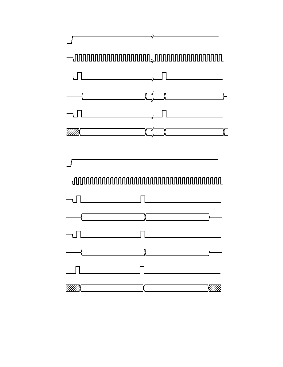
SAMPLE WORD (DEVICE 1)
SAMPLE WORD (DEVICE 1)
SDO
SCLK
SDIFS
SDI
DATA (CONTROL) WORD (DEVICE 1)
DATA (CONTROL) WORD (DEVICE 1)
Figure 10. Interface Signal Timing for Single Device Operation
SAMPLE WORD (DEVICE 2)
SAMPLE WORD (DEVICE 1)
SAMPLE WORD (DEVICE 1)
DATA (CONTROL) WORD (DEVICE 2)
DATA (CONTROL) WORD (DEVICE 2)
DATA (CONTROL) WORD (DEVICE 1)
SE
SDOFS(2)
SDO(2)
SCLK
SDOFS(1)
SDIFS(2)
SDO(1)
SDI(2)
SDIFS(1)
SDI(1)
Figure 11. Interface Signal Timing for Cascade of Two Devices
AD73311
21
REV. B
Cascade Operation
The AD73311 has been designed to support up to eight codecs
in a cascade connected to a single serial port, see Figure 31.
The SPORT interface protocol has been designed so that device
addressing is built into the packet of information sent to the
device. This allows the cascade to be formed with no extra hard-
ware overhead for control signals or addressing. A cascade can
be formed in either of the two modes previously discussed.
There may be some restrictions in cascade operation due to the
number of devices configured in the cascade and the serial clock
rate chosen. Table XVI details the requirements for SCLK rate
for cascade lengths from 1 to 8 devices. This assumes a directly
coupled frame sync arrangement as shown in Figure 13.
Table XVI. Cascade Options
Number of Devices in Cascade
SCLK
1
2
3
4
5
6
7
8
DMCLK
DMCLK/2
DMCLK/4
X
X
X
X
DMCLK/8
X
X
X
X
X
X
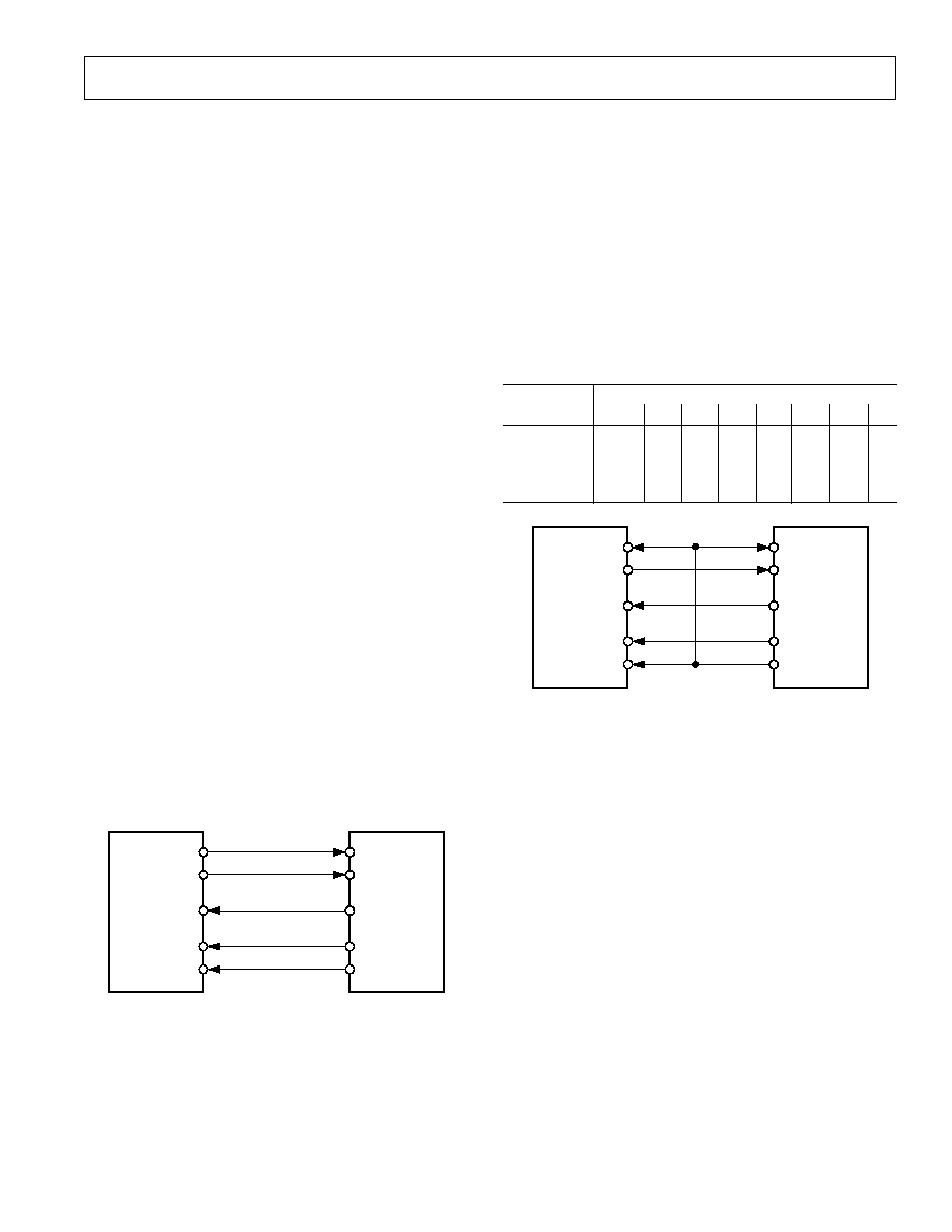
AD73311
CODEC
SDIFS
SDI
SCLK
SDO
SDOFS
TFS
DT
SCLK
DR
RFS
ADSP-21xx
DSP
Figure 13. Directly Coupled or Frame Sync Loop-
Back Configuration
When using the indirectly coupled frame sync configuration in
cascaded operation it is necessary to be aware of the restrictions
in sending data to all devices in the cascade. Effectively the time
allowed is given by the sampling interval (256/DMCLK) which
is 15.625
µs for a sample rate of 64 kHz. In this interval, the
DSP must transfer N
× 16 bits of information where N is the
number of devices in the cascade. Each bit will take 1/SCLK
and, allowing for any latency between the receipt of the Rx
interrupt and the transmission of the Tx data, the relationship
for successful operation is given by:
256/DMCLK > ((N/SCLK) + T
INTERRUPT LATENCY
)
The interrupt latency will include the time between the ADC
sampling event and the Rx interrupt being generated in the
DSP--this should be 16 SCLK cycles.
In Cascade Mode, each device must know the number of
devices in the cascade because the Data and Mixed modes use a
method of counting input frame sync pulses to decide when they
should update the DAC register from the serial input register.
INTERFACING
The AD73311 can be interfaced to most modern DSP engines
using conventional serial port connections and an extra enable
control line. Both serial input and output data use an accompa-
nying frame synchronization signal which is active high one
clock cycle before the start of the 16-bit word or during the last
bit of the previous word if transmission is continuous. The serial
clock (SCLK) is an output from the codec and is used to define
the serial transfer rate to the DSP's Tx and Rx ports. Two primary
configurations can be used: the first is shown in Figure 12 where
the DSP's Tx data, Tx frame sync, Rx data and Rx frame sync
are connected to the codec's SDI, SDIFS, SDO and SDOFS
respectively. This configuration, referred to as indirectly coupled
or nonframe sync loop-back, has the effect of decoupling the
transmission of input data from the receipt of output data. The
delay between receipt of codec output data and transmission of
input data for the codec is determined by the DSP's software
latency. When programming the DSP serial port for this con-
figuration, it is necessary to set the Rx FS as an input and the
Tx FS as an output generated by the DSP. This configuration is
most useful when operating in mixed mode, as the DSP has the
ability to decide how many words (either DAC or control) can be
sent to the codec(s). This means that full control can be imple-
mented over the device configuration as well as updating the
DAC in a given sample interval. The second configuration
(shown in Figure 13) has the DSP's Tx data and Rx data con-
nected to the codec's SDI and SDO, respectively while the
DSP's Tx and Rx frame syncs are connected to the codec's
SDIFS and SDOFS. In this configuration, referred to as directly
coupled or frame sync loop-back, the frame sync signals are
connected together and the input data to the codec is forced to
be synchronous with the output data from the codec. The DSP
must be programmed so that both the Tx FS and Rx FS are
inputs as the codec SDOFS will be input to both. This configu-
ration guarantees that input and output events occur simulta-
neously and is the simplest configuration for operation in
normal Data Mode. Note that when programming the DSP in
this configuration it is advisable to preload the Tx register with
the first control word to be sent before the codec is taken out of
reset. This ensures that this word will be transmitted to coincide
with the first output word from the device(s).
AD73311
CODEC
SDIFS
SDI
SCLK
SDO
SDOFS
TFS
DT
SCLK
DR
RFS
ADSP-21xx
DSP
Figure 12. Indirectly Coupled or Nonframe Sync Loop-
Back Configuration
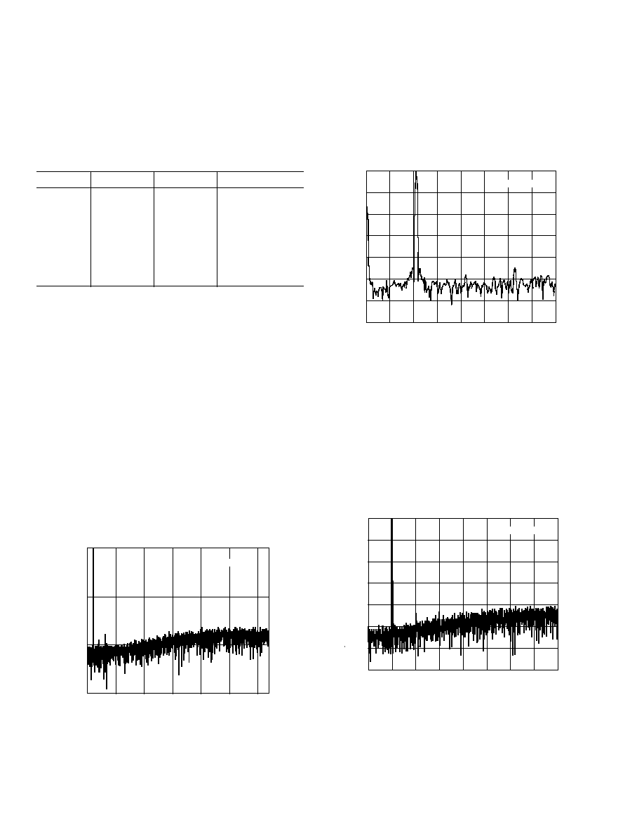
AD73311
22
REV. B
Control Register A contains a 3-bit field (DC02) that is pro-
grammed by the DSP during the programming phase. The default
condition is that the field contains 000b, which is equivalent to
a single device in cascade (see Table XVII). However, for
cascade operation this field must contain a binary value that is
one less than the number of devices in the cascade.
Table XVII. Device Count Settings
DC2
DC1
DC0
Cascade Length
0
0
0
1
0
0
1
2
0
1
0
3
0
1
1
4
1
0
0
5
1
0
1
6
1
1
0
7
1
1
1
8
PERFORMANCE
As the AD73311 is designed to provide high performance, low
cost conversion, it is important to understand the means by
which this high performance can be achieved in a typical applica-
tion. This section will, by means of spectral graphs, outline the
typical performance of the device and highlight some of the
options available to users in achieving their desired sample
rate, either directly in the device or by doing some post-processing
in the DSP, while also showing the advantages and disadvan-
tages of the different approaches.
Encoder Section
The encoder section samples at DMCLK/256, which gives a
64 kHz output rate for DMCLK equal to 16.384 MHz. The
noise shaping of the sigma-delta modulator also depends on the
frequency at which it is clocked, which means that the best
dynamic performance in a particular bandwidth is achieved by
oversampling at the highest possible rate. If we assume that the
signals of interest are in the voice bandwidth of dc4 kHz, then
sampling at 64 kHz gives a spectral response which ensures good
SNR performance in the voice bandwidth, as shown in Figure 14.
FREQUENCY kHz
0
60
150
0
32
5
dB
10
15
20
25
30
100
S/N+D = 59.4951
Figure 14. FFT (ADC 64 kHz Sampling)
If sampling at 8 kHz is required, the user must implement some
post-processing in the DSP engine to band limit the signal and
decimate the samples to achieve the ultimate sampling rate of
8 kHz. Figure 15 shows the final spectral response of the
64 kHz sampled data having been digitally filtered and deci-
mated to an 8 kHz rate. The filter used was a 6th order ellip-
tical filter.
FREQUENCY kHz
0
140
0
4.0
0.5
dB
1.0
1.5
2.0
2.5
3.0
3.5
20
60
80
100
120
40
S/N+D = 80.615918
Figure 15. FFT (ADC 8 kHz Filtered and Decimated from
64 kHz)
The device features an on-chip master clock divider circuit that
allows the sample rate to be reduced. The present choice of
clock divider options permits the device to sample at 64 kHz,
32 kHz, 21.33 kHz, 16 kHz and 12.8 kHz from a 16.384 MHz
master clock. Reducing the DMCLK rate lowers the sampling
rate of the sigma-delta modulator, which causes the noise shaping
to occur in a reduced bandwidth. The SNR performance up to
F
S
/2 will still be similar to that in the case of 64 kHz sampling,
but will be disimproved in the voice bandwidth due to the re-
duced noise shaping. Figure 16 shows this effect for a sampling
rate of 16 kHz.
FREQUENCY kHz
0
140
0
8
1
dB
2
3
4
5
6
7
20
60
80
100
120
40
S/N+D = 59.162677
Figure 16. FFT (ADC 16 kHz Sampling)
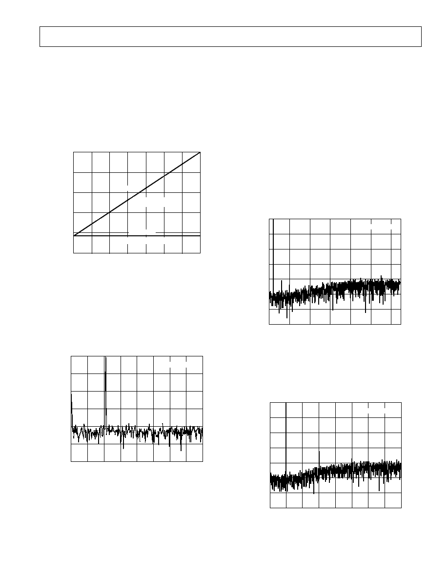
AD73311
23
REV. B
In order to produce a direct sampling rate of 8 kHz, it is
necessary to reduce the external master clock to 8.192 MHz and
to set the master clock divider to a ratio of 4, which results in a
sample rate of 8 kHz. In this case, the response of the Sinc
3
decimation filter may affect the response in the voice BW as its
first null occurs at 8 kHz. In Figure 17, Trace A shows how the
SNR remains approximately constant up to F
S
/2 regardless of
the sample rate F
S
; Trace B shows that the SNR achievable in
the voice BW is proportional to the sampling rate F
S
. These two
traces intersect at an F
S
of 8 kHz which is the point where F
S
/2
equals the voice BW.
SAMPLING FREQUENCY (DMCLK/256) kHz
8
16
24
32
40
48
56
64
80
70
S/(N+D)
dB
65
55
75
60
SNR IN VOICEBAND
(300Hz3400Hz)
SNR IN BAND UP TO F
S
/2
TRACE B
TRACE A
Figure 17. SNR vs. Sampling Frequency
If the input signal is externally band-limited, it is possible to
achieve the 8 kHz sampling rate directly from the 64 kHz
sample rate by decimating the sampled data in the DSP. This
technique will alias the band between 8 kHz and 64 kHz into
the 8 kHz band, therefore it is necessary to have good quality
external band-limiting on the input signal. Figure 18 shows the
spectral response of using this decimation technique for sample
rate reduction.
FREQUENCY kHz
0
120
0
4.0
0.5
dB
1.0
1.5
2.0
2.5
3.0
3.5
20
60
80
100
40
S/N+D = 59.545
Figure 18. FFT (ADC 8 kHz Subsampled)
Encoder Group Delay
The AD73311 implementation offers a very low level of group
delay, which is given by the following relationship:
Group Delay (Decimator) = Order
× ((M1)/2) × Tdec
where:
Order is the order of the decimator (= 3),
M is the decimation factor (= 32) and
Tdec is the decimation sample interval (= 1/2.048e6)
=> Group Delay (Decimator) = 3
× (321)/2 × (1/2.048e6)
= 22.7
µs
If final filtering is implemented in the DSP, the final filter's
group delay must be taken into account when calculating overall
group delay.
Decoder Section
The decoder section updates (samples) at the same rate as the
encoder section, MCLK/256, which gives a 64 kHz rate from an
external MCLK of 16.384 MHz. Figure 19 shows the spectral
response of the decoder section sampling at 64 kHz. Again, its
sigma-delta modulator shapes the noise so it is reduced in the
voice bandwidth dc4 kHz. For improved voiceband SNR, the
user can implement an initial anti-imaging filter, preceded by
8 kHz to 64 kHz interpolation, in the DSP.
FREQUENCY kHz
0
140
0
32
5
dB
10
15
20
25
30
20
60
80
100
120
40
S/N+D = 58.454842
Figure 19. FFT (DAC 64 kHz Sampling)
As is the case with the encoder section, voiceband SNR is re-
duced if the DMCLK rate is reduced as shown by the example
of 16 kHz sampling in Figure 20. This is due to the noise-shap-
ing of the sigma-delta modulator being compressed into a
smaller bandwidth, which increases the noise in the voice BW.
FREQUENCY kHz
0
140
0
8
1
2
3
4
5
6
7
20
60
80
100
120
40
dB
S/N+D = 57.441659
Figure 20. FFT (DAC 16 kHz Sampling)
AD73311
24
REV. B
It is also possible to subsample the DAC--update at a lower rate
than the sampling rate--to reduce the overhead on the DSP.
This, however, results in imaging of the subsampled bandwidth
into the normal bandwidth, which implies that higher perfor-
mance external anti-imaging filtering must be used to eliminate
the images.
The interpolator input also provides a minimum group delay
realization in situations where that is critical. Further reduction
in group delay is possible by accessing the digital sigma-delta
input at the expense of lower attenuation of images due to any
repetition of input samples. Figure 21 shows the spectral
response of the decoder being sampled at 64 kHz with its inter-
polator bypassed.
FREQUENCY kHz
0
140
0
32
5
10
15
20
25
30
20
60
80
100
120
40
dB
S/N+D = 58.557732
Figure 21. FFT (DAC 64 kHz Sampling--Interpolator
Bypassed)
Decoder Group Delay
The interpolator roll-off is mainly due to its sync-cubed function
characteristic, which has an inherent group delay given by the
equation.
Group Delay (Interpolator) = Order
× (L 1)/2) × Tint
where:
Order is the interpolator order (= 3),
L is the interpolation factor (= 32) and
Tint is the interpolation sample interval
(= 1/2.048e6)
=> Group Delay (Interpolator)
= 3*(32-1)/2*(1/2.048e6)
= 22.7
µs
The analog section has a group delay of approximately 25
µs.
DESIGN CONSIDERATIONS
Analog Input
The analog input signal to the codec can be dc coupled, pro-
vided that the dc bias level of the input signal is the same as the
internal reference level (REFOUT). Figure 22 shows the recom-
mended differential input circuit for the AD73311's analog
input pins (VIN). The circuit of Figure 22 implements first-
order low-pass filters with a 3 dB point at 34 kHz; these are the
only filters that must be implemented external to the AD73311
to prevent aliasing of the sampled signal. Since the codec's ADC
uses a highly oversampled approach that transfers the bulk of
the antialiasing filtering into the digital domain, the off-chip
antialiasing filter need only be of a low order. It is recommended
that for optimum performance that the capacitors used for the
antialiasing filter be of high quality dielectric (NPO).
REFCAP
VOLTAGE
REFERENCE
0.1 F
REFOUT
TO INPUT BIAS
CIRCUITRY
100
100
V
IN
0.047 F
0.047 F
VINN
VINP
AD73311
Figure 22. Example Circuit for Differential Input
(DC Coupling)
The AD73311's on-chip 38 dB preamplifier can be enabled when
there is not enough gain in the input circuit; the preamplifier is
configured by bits IGS02 of CRD. The total gain must be
configured to ensure that a full-scale input signal produces a
signal level at the input to the sigma-delta modulator of the
ADC that does not exceed the maximum input range.
The dc biasing of the analog input signal is accomplished with
an on-chip voltage reference. If the input signal is not biased at
the internal reference level (via REFOUT), then it must be ac-
coupled with external coupling capacitors. C
IN
should be 0.1
µF
or larger. The dc biasing of the input can then be accomplished
using resistors to REFOUT as in Figure 23.
REFCAP
VOLTAGE
REFERENCE
0.1 F
REFOUT
TO INPUT BIAS
CIRCUITRY
100
100
V
IN
CIN
CIN
0.047 F
0.047 F
VINN
VINP
10k
10k
AD73311
Figure 23. Example Circuit for Differential Input
(AC Coupling)
AD73311
25
REV. B
REFCAP
VOLTAGE
REFERENCE
0.1 F
REFOUT
V
IN
0.047 F
VINN
VINP
100
CIN
10k
AD73311
Figure 25. Example Circuit for Single-Ended Input
(AC Coupling)
Analog Output
The AD73311's differential analog output (VOUT) is produced
by an on-chip differential amplifier. The differential output
can be ac-coupled or dc-coupled directly to a load or to an
external amplifier. Figure 26 shows a simple circuit providing
a differential output with ac coupling. The capacitors in this
circuit (C
OUT
) are optional; if used, their value can be chosen
as follows:
C
OUT
=
1
2
f
C
R
L
where f
C
= desired cutoff frequency.
AD73311
R
L
VOUTP
VOUTN
(VOUT CHANNEL)
C
OUT
C
OUT
Figure 26. Example Circuit for Differential Output
Figure 27 shows an example circuit for providing a single-ended
output with ac coupling. The capacitor of this circuit (C
OUT
) is
not optional if dc current drain is to be avoided.
R
L
VOUTP
(VOUT CHANNEL)
C
OUT
VOUTN
AD73311
Figure 27. Example Circuit for Single-Ended Output
Digital Interfacing
The AD73311 is designed to easily interface to most common
DSPs. The SCLK, SDO, SDOFS, SDI and SDIFS must be
connected to the SCLK, DR, RFS, DT and TFS pins of the
DSP respectively. The SE pin may be controlled from a parallel
output pin or flag pin such as FL02 on the ADSP-21xx (or XF
on the TMS320C5x) or, where SPORT powerdown is not
required, it can be permanently strapped high using a suitable
pull-up resistor. The
RESET pin may be connected to the sys-
tem hardware reset structure or it may also be controlled using a
dedicated control line. In the event of tying it to the global sys-
tem reset, it is necessary to operate the device in mixed mode,
which allows a software reset, otherwise there is no convenient
way of resetting the device. Figures 28 and 29 show typical
connections to an ADSP-2181 and TMS320C5x respectively.
SDIFS
SDI
SCLK
SDO
SDOFS
TFS
DT
SCLK
DR
RFS
RESETB
SE
FL0
FL1
ADSP-21xx
DSP
AD73311
CODEC
Figure 28. AD73311 Connected to ADSP-2181
SDIFS
SDI
SCLK
SDO
SDOFS
FSX
DX
CLKX
CLKR
DR
RESETB
SE
FSR
XF
TMS320C5x
DSP
AD73311
CODEC
Figure 29. AD73311 Connected to TMS320C5x
Figures 24 and 25 detail dc- and ac-coupled input circuits for
single-ended operation respectively.
REFCAP
VOLTAGE
REFERENCE
0.1 F
REFOUT
V
IN
0.047 F
VINN
VINP
100
AD73311
Figure 24. Example Circuit for Single-Ended Input
(DC Coupling)
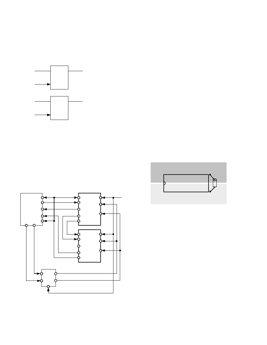
AD73311
26
REV. B
Cascade Operation
Where it is required to configure a cascade of up to eight de-
vices, it is necessary to ensure that the timing of the SE and
RESET signals is synchronized at each device in the cascade. A
simple D type flip flop is sufficient to sync each signal to the
master clock MCLK, as in Figure 30.
1/2
74HC74
D
CLK
Q
DSP CONTROL
TO SE
MCLK
SE SIGNAL SYNCHRONIZED
TO MCLK
DSP CONTROL
TO
RESET
MCLK
RESET SIGNAL SYNCHRONIZED
TO MCLK
1/2
74HC74
D
CLK
Q
Figure 30. SE and
RESET Sync Circuit for Cascaded
Operation
Connection of a cascade of devices to a DSP, as shown in Fig-
ure 31, is no more complicated than connecting a single device.
Instead of connecting the SDO and SDOFS to the DSP's Rx
port, these are now daisy-chained to the SDI and SDIFS of the
next device in the cascade. The SDO and SDOFS of the final
device in the cascade are connected to the DSP's Rx port to
complete the cascade. SE and
RESETB on all devices are fed
from the signals that were synchronized with the MCLK using
the circuit as described above. The SCLK from only one device
need be connected to the DSP's SCLK input(s) as all devices
will be running at the same SCLK frequency and phase.
SDIFS
SDI
SCLK
SDO
SDOFS
TFS
DT
SCLK
DR
RFS
MCLK
SE
RESET
DEVICE 1
FL0
FL1
SDIFS
SDI
SCLK
SDO
SDOFS
MCLK
SE
RESET
DEVICE 2
74HC74
D1
D2
Q1
Q2
CLK
AD73311
CODEC
AD73311
CODEC
ADSP-2181
DSP
Figure 31. Connection of Two AD73311s Cascaded to
ADSP-2181
Grounding and Layout
Since the analog inputs to the AD73311 are differential, most of
the voltages in the analog modulator are common-mode volt-
ages. The excellent common-mode rejection of the part will
remove common-mode noise on these inputs. The analog and
digital supplies of the AD73311 are independent and separately
pinned out to minimize coupling between analog and digital
sections of the device. The digital filters on the encoder section
will provide rejection of broadband noise on the power supplies,
except at integer multiples of the modulator sampling frequency.
The digital filters also remove noise from the analog inputs
provided the noise source does not saturate the analog modula-
tor. However, because the resolution of the AD73311's ADC is
high, and the noise levels from the AD73311 are so low, care
must be taken with regard to grounding and layout.
The printed circuit board that houses the AD73311 should be
designed so the analog and digital sections are separated and
confined to certain sections of the board. The AD73311 pin
configuration offers a major advantage in that its analog and
digital interfaces are connected on opposite sides of the package.
This facilitates the use of ground planes that can be easily sepa-
rated, as shown in Figure 32. A minimum etch technique is
generally best for ground planes as it gives the best shielding.
Digital and analog ground planes should be joined in only one
place. If this connection is close to the device, it is recom-
mended to use a ferrite bead inductor as shown in Figure 32.
DIGITAL GROUND
ANALOG GROUND
Figure 32. Ground Plane Layout
Avoid running digital lines under the device for they will couple
noise onto the die. The analog ground plane should be allowed
to run under the AD73311 to avoid noise coupling. The power
supply lines to the AD73311 should use as large a trace as pos-
sible to provide low impedance paths and reduce the effects of
glitches on the power supply lines. Fast switching signals such as
clocks should be shielded with digital ground to avoid radiating
noise to other sections of the board, and clock signals should
never be run near the analog inputs. Traces on opposite sides of
the board should run at right angles to each other. This will
reduce the effects of feedthrough through the board. A microstrip
technique is by far the best but is not always possible with a
double-sided board. In this technique, the component side of
the board is dedicated to ground planes while signals are placed
on the other side.

AD73311
27
REV. B
Good decoupling is important when using high speed devices.
All analog and digital supplies should be decoupled to AGND
and DGND respectively, with 0.1
µF ceramic capacitors in
parallel with 10
µF tantalum capacitors. To achieve the best
from these decoupling capacitors, they should be placed as close
as possible to the device, ideally right up against it. In systems
where a common supply voltage is used to drive both the AVDD
and DVDD of the AD73311, it is recommended that the
system's AVDD supply be used. This supply should have the
recommended analog supply decoupling between the AVDD
pins of the AD73311 and AGND and the recommended digital
supply decoupling capacitors between the DVDD pin and
DGND.
DSP Programming Considerations
This section discusses some aspects of how the serial port of the
DSP should be configured and the implications of whether Rx
and Tx interrupts should be enabled.
DSP SPORT Configuration
Following are the key settings of the DSP SPORT required for
the successful operation with the AD73311:
· Configure for external SCLK.
· Serial Word Length = 16 bits.
· Transmit and Receive Frame Syncs required with every word.
· Receive Frame Sync is an input to the DSP.
· Transmit Frame Sync is an:
Input--in Frame Sync Loop-Back Mode
Output--in Nonframe Sync Loop-Back Mode.
· Frame Syncs occur one SCLK cycle before the MSB of the
·
serial word.
· Frame Syncs are active high.
DSP SPORT Interrupts
If SPORT interrupts are enabled, it is important to note that the
active signals on the frame sync pins do not necessarily corre-
spond with the positions in time of where SPORT interrupts are
generated.
On ADSP-21xx processors, it is necessary to enable SPORT
interrupts and use Interrupt Service Routines (ISRs) to handle
Tx/Rx activity, while on the TMS320CSx processors it is pos-
sible to poll the status of the Rx and Tx registers, which means
that Rx/Tx activity can be monitored using a single ISR that
would ideally be the Tx ISR as the Tx interrupt will typically
occur before the Rx ISR.
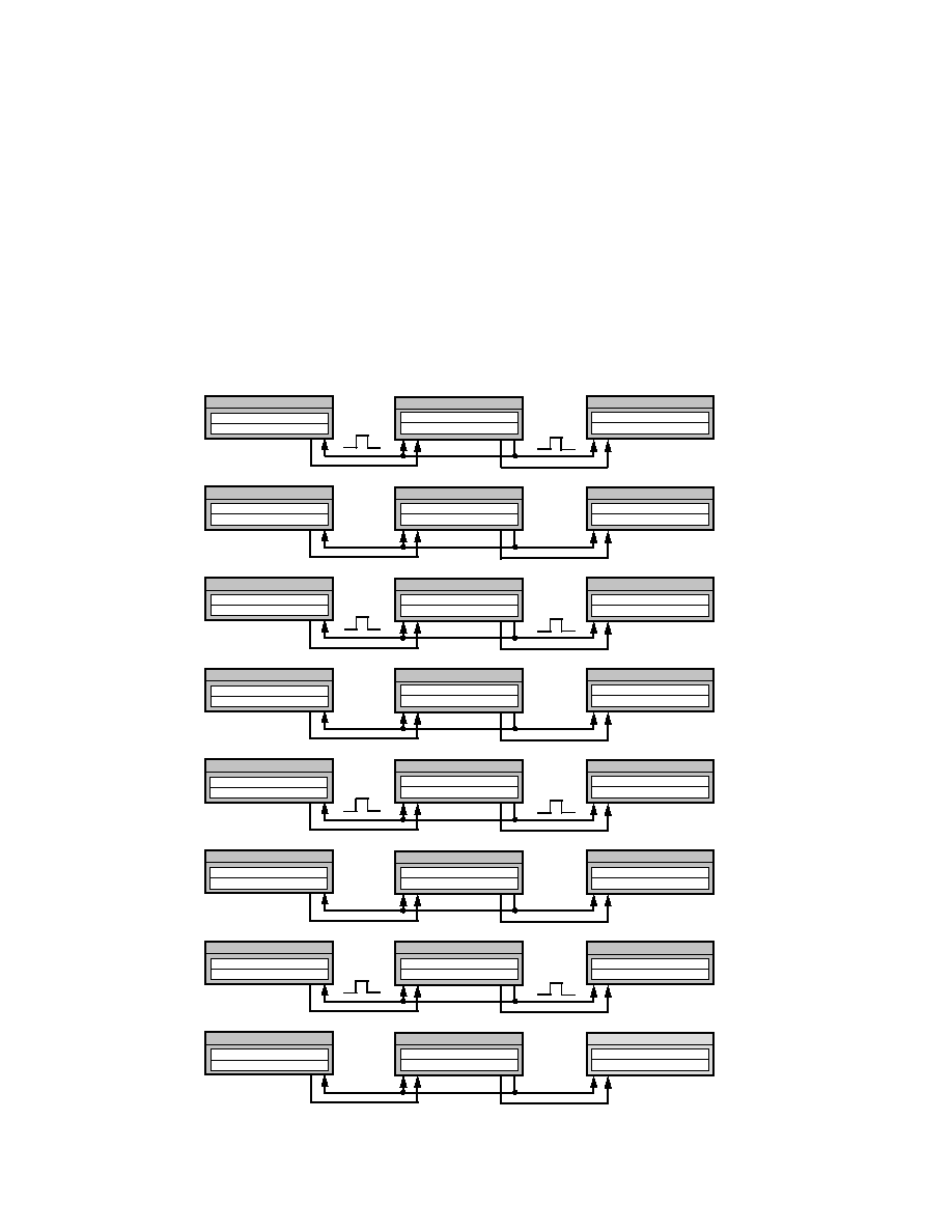
AD73311
28
REV. B
APPENDIX A
Programming a Single AD73311 for Data Mode Operation
This section describes a typical sequence in programming a
single codec to operate in normal DATA mode. It details the
control (program) words that are sent to the device to configure
its internal registers and shows the typical output data received
during both program and data modes. The device is connected
in Frame Sync Loop-Back Mode (see Figure 13), which forces
an input word from the DSP's Tx Reg each time the codec
outputs a word via the SDO/SDOFS lines. In Step 1, the part
has just been reset and on the first output event the codec pre-
sents an invalid output word
1
. The DSP's Tx Reg contains a
DSP TX REG
CONTROL WORD 1
1 0 000 001 00000011
ADC WORD 1 *
0000 0000 0000 0000
DON'T CARE
XXXX XXXX XXXX XXXX
DSP RX REG
STEP 1
DSP TX REG
DEVICE 1
CONTROL WORD 1
1 0 000 010 00000001
CONTROL WORD 1
1 0 000 001 00000011
ADC WORD 1 *
0000 0000 0000 0000
DSP RX REG
STEP 2
DSP TX REG
DEVICE 1
CONTROL WORD 1
1 0 000 010 00000001
ADC WORD 1 *
1011 1001 0000 0011
DON'T CARE
XXXX XXXX XXXX XXXX
DSP RX REG
STEP 3
DSP TX REG
DEVICE 1
CONTROL WORD 1
1 0 000 000 00000001
CONTROL WORD 1
1 0 000 010 00000001
ADC WORD 1 *
1011 1001 0000 0011
DSP RX REG
STEP 4
DSP TX REG
DEVICE 1
CONTROL WORD 1
1 0 000 000 00000001
ADC WORD 1 *
1011 1010 0000 0001
DON'T CARE
XXXX XXXX XXXX XXXX
DSP RX REG
STEP 5
DSP TX REG
DEVICE 1
DAC WORD 1
0111 1111 1111 1111
CONTROL WORD 1
1 0 000 000 00000001
ADC WORD 1 *
1011 1010 0000 0001
DSP RX REG
STEP 6
DSP TX REG
DAC WORD 1
0111 1111 1111 1111
ADC WORD 1
1000 0000 0000 0000
DON'T CARE
XXXX XXXX XXXX XXXX
DSP RX REG
STEP 7
DSP TX REG
DEVICE 1
DAC WORD 1
0111 1111 1111 1111
DAC WORD 1
0111 1111 1111 1111
ADC WORD 1
1000 0000 0000 0000
DSP RX REG
STEP 8
*ADC SAMPLES DURING PROGRAM MODE ARE INVALID.
DEVICE 1
DEVICE 1
Figure 33. Programming a Single AD73311 for Normal
control word that programs CRB with the data word 0x03. In
Step 2, the control word from the DSP's Tx Reg has been sent
to the codec's SPORT and the output word has been received
by the DSP's Rx Reg. In Steps 3 and 4, register CRC is pro-
grammed with 0x01, which powers up the analog section. In
Steps 5 and 6, the codec is put into programming mode by
setting the
PGM/DATA bit of CRA. In Step 7, the output word
from the device is now a valid ADC word as the device has been
programmed into data mode. Note also that the codec now
expects DAC data to be sent to it and will interpret any data
from the DSP to be 16-bit DAC data.
NOTE
1
Data output by the codec in program mode is invalid and should not be inter-
preted as ADC data. The only exception to this is output caused by register
reads or CEE being enabled on control word writes.
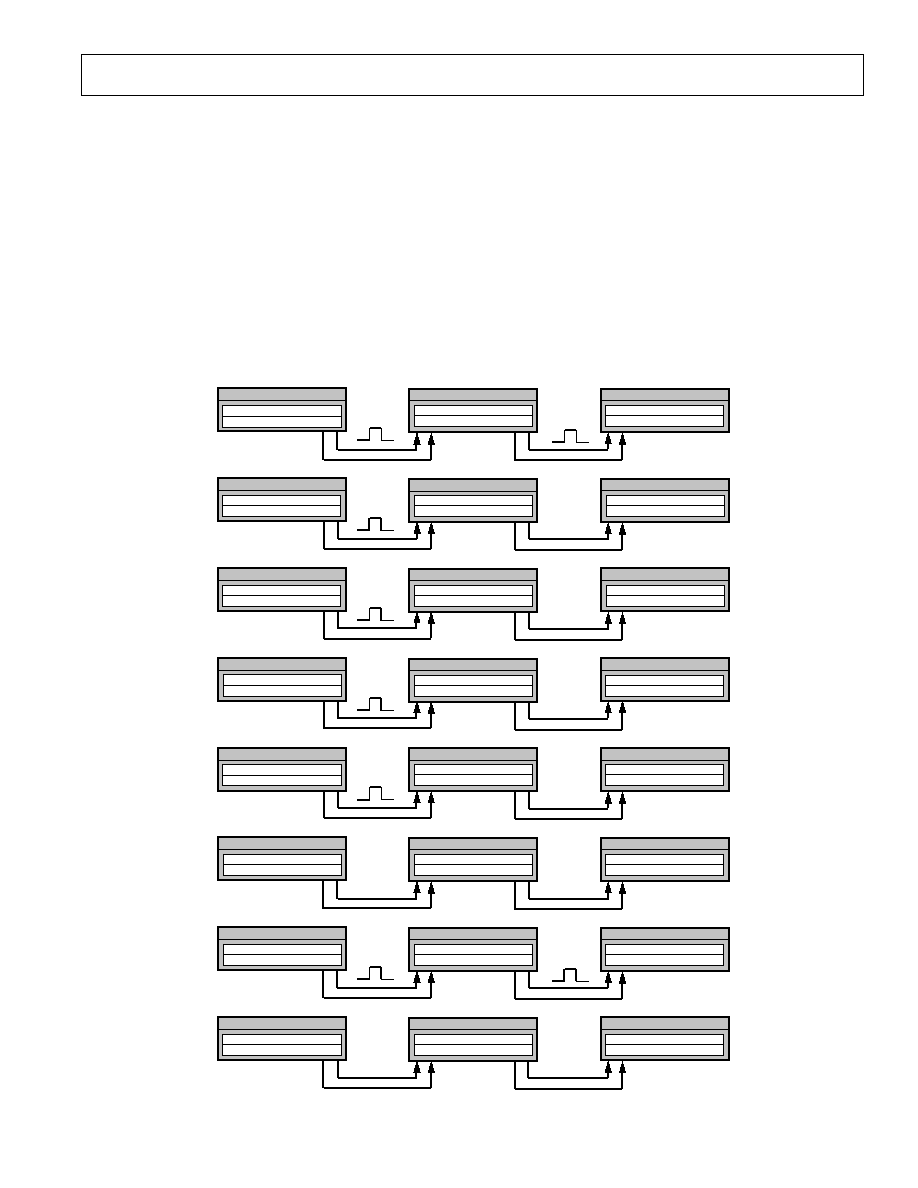
AD73311
29
REV. B
APPENDIX B
Programming a Single AD73311 for Mixed Mode Operation
This section describes a typical sequence in programming a
single codec to operate in mixed mode. The device is connected
in Nonframe Sync Loop-Back Mode (see Figure 14), which
allows the DSP's Tx Reg to determine how many words are sent
to the device. In Step 1, the part has just been reset and on the
first output event the codec presents an invalid output word
1
.
The DSP's Tx Reg contains a control word that programs CRA
with the data word 0x03, which will put the device in mixed
mode. In Step 2, the control word from the DSP's Tx Reg has
been sent to the codec's SPORT and the output word has been
received by the DSP's Rx Reg. The Tx Register raises the
SDIFS to send a control word that will program CRB of the
codec. In Step 3 the SCLK and sample rate are set by program-
ming CRB. In Step 4, the analog sections of the device are
powered up by programming CRC, while in Step 5, the encoder
gain is set to 0 dB via CRD. In Step 6, the DAC register is
updated by the contents of the serial register. Alternately, a
register read cycle could be introduced instead of the DAC load
in Step 6
2
. Steps 7 and 8 show another ADC read, DAC write
cycle.
NOTES
1
Data output by the codec in program mode is invalid and should not be inter-
preted as ADC data. The only exception to this is output caused by register
reads or CEE being enabled on control word writes.
2
In mixed mode, it may be necessary to terminate a control word write to a
device with a control word read to that device in order to ensure that the next
ADC sample is correct. Alternatively the ADC word can either be discarded or,
if this is not possible, it can be rebuilt by incrementing the "address field"
within the 16-bit word.
DSP TX REG
CONTROL WORD 1
1 0 000 000 00000011
ADC WORD 1 *
0000 0000 0000 0000
DON'T CARE
XXXX XXXX XXXX XXXX
STEP 1
DSP TX REG
DEVICE 1
CONTROL WORD 1
1 0 000 001 00001111
CONTROL WORD 1
1 0 000 000 00000011
ADC WORD 1 *
0000 0000 0000 0000
DSP RX REG
STEP 2
DSP TX REG
DEVICE 1
CONTROL WORD 1
1 0 000 010 00000001
CONTROL WORD 1
1 0 000 001 00001111
DON'T CARE
XXXX XXXX XXXX XXXX
DSP RX REG
STEP 3
DSP TX REG
DEVICE 1
CONTROL WORD 1
1 0 000 000 00000001
CONTROL WORD 1
1 0 000 010 00000001
DON'T CARE
XXXX XXXX XXXX XXXX
DSP RX REG
STEP 4
DSP TX REG
DEVICE 1
DAC WORD 1
0100 0000 0000 0000
CONTROL WORD 1
1 0 000 011 00100000
DON'T CARE
XXXX XXXX XXXX XXXX
DSP RX REG
STEP 5
DSP TX REG
DEVICE 1
DAC WORD 1
0011 1111 1111 1111
DAC WORD 1
0100 0000 0000 0000
DON'T CARE
XXXX XXXX XXXX XXXX
DSP RX REG
STEP 6
DSP TX REG
DAC WORD 1
0011 1111 1111 1111
ADC WORD 1
0100 0000 0000 0000
DON'T CARE
XXXX XXXX XXXX XXXX
DSP RX REG
STEP 7
DSP TX REG
DEVICE 1
DAC WORD 1
0100 0000 0000 0000
DAC WORD 1
0011 1111 1111 1111
ADC WORD 1
1000 0000 0000 0000
DSP RX REG
STEP 8
*ADC SAMPLES DURING PROGRAM MODE ARE INVALID.
DEVICE 1
DSP RX REG
DEVICE 1
Figure 34. Programming a Single AD73311 for Mixed Mode

AD73311
30
REV. B
APPENDIX C
Configuring a Cascade of Two AD73311s to Operate in
Data Mode
This section describes a typical sequence of control words that
would be sent to a cascade of two AD73311s to set them up for
operation. It is not intended to be a definitive initialization
sequence, but will show users the typical input/output events
that occur in the programming and operation phases
1
. This
description panel refers to Figure 35.
In Step 1, we have the first output sample event following device
reset. The SDOFS signal is raised on both devices simulta-
neously, which prepares the DSP Rx register to accept the ADC
word from Device 2, while SDOFS from Device 1 becomes an
SDIFS to Device 2. As the SDOFS of Device 2 is coupled to
the DSP's TFS and RFS, and to the SDIFS of Device 1, this
event also forces a new control word to be output from the DSP
Tx register to Device 1.
In Step 2, we observe the status of the devices following the
transmission of the first control word. The DSP has received the
ADC word from Device 2, while Device 2 has received the
ADC word from Device 1 and Device 1 has received the Con-
trol word destined for Device 2. At this stage, the SDOFS of
both devices are again raised because Device 2 has received
Device 1's ADC word, and as it is not a valid control word
addressed to Device 2, it is passed on to the DSP. Likewise,
Device 1 has received a control word destined for Device 2--
address field is not zero--and it decrements the address field of
the control word and passes it on.
Step 3 shows completion of the first series of control word
writes. The DSP has now received both invalid ADC words and
each device has received a control word that addresses control
register B and sets the internal MCLK divider ratio to 1, SCLK
rate to DMCLK/8. Note that both devices are updated simulta-
neously as both receive the addressed control word at the same
time. This is an important factor in cascaded operation as any
latency between updating the SCLK or DMCLK of devices can
result in corrupted operation. This will not happen in the case
of a FSLB configuration as shown here, but must be taken into
account in a non-FSLB configuration. One other important
observation of this sequence is that the data words are received
and transmitted in reverse order, i.e., the ADC words are
received by the DSP, Device 2 first, then Device 1, and similarly
the transmit words from the DSP are sent Device 2 first, then
Device 1. This ensures that all devices are updated at the same
time.
In Step 4, the next ADC sample event that happens raises the
SDOFS lines of each of the devices. The DSP Tx register con-
tains the first of the two control words to be written to the cas-
cade--the word for Device 2.
In Step 5, following transmission of the first of the two control
words, the DSP Rx register contains Device 2's ADC word,
Device 2's serial register contains the Device 1 ADC word,
Device 1's serial register contains the control word addressed to
Device 2 and the DSP Tx register contains the next control
word--that addressed to Device 1. Again, both devices raise
their SDOFS lines as both have received control words not
addressed to them.
Step 6 shows the completion of the second set of control word
writes. In this case, both devices have received a control word
addressed to control register A, which sets the device count field
equal to two devices in cascade and sets the
PGM/DATA bit to
one to put the device in data mode.
In Step 7, the programming phase is complete and we now
begin actual device data read and write. The words loaded into
the serial registers of the two devices at the ADC sampling event
now contain valid ADC data and the words written to the de-
vices from the DSP's Tx register will now be interpreted as
DAC words. Note, therefore, that the DSP Tx register contains
the DAC word for Device 2.
In Step 8, the first DAC word has been transmitted into the
cascade and the ADC word from Device 2 has been read from
the cascade. The DSP Tx register now contains the DAC word
for Device 1. As the words being sent to the cascade are now
being interpreted as 16-bit DAC words, the addressing scheme
now changes from one where the address was embedded in the
transmitted word to one where the serial port now counts the
SDIFS pulses. When the number of SDIFS pulses received
equals the value in the device count field of control register A--
the length of the cascade--each device updates its DAC register
with the present word in its serial register. In Step 8 each device
has received only one SDIFS pulse; Device 2 received one
SDIFS from the SDOFS of Device 1 when it sent its ADC word
and Device 1 received one SDIFS pulse when it received the
DAC word for Device 2 from the DSP's Tx register. Therefore,
each device raises its SDOFS line to pass on the current word in
its serial register, and each device now receives another SDIFS
pulse.
Step 9 shows the completion of an ADC read and DAC write
cycle. Following Step 8, each device has received two SDIFS
pulses that equal the setting of the device count field in Control
Register A. The DAC register in each device is now updated
with the contents of the word that accompanied the SDIFS
pulse which satisfied the device count requirement. The internal
frame sync counter is now reset to zero and will begin counting
for the next DAC update cycle.
NOTE
1
This sequence assumes that the DSP SPORT's Rx and Tx interrupts are enabled.
It is important to ensure that there is no latency (separation) between control
words in a cascade configuration. This is especially the case when programming
Control Register B as it contains settings for SCLK and DMCLK rates.
AD73311
31
REV. B
DSP TX REG
DEVICE 1
DEVICE 2
CONTROL WORD 2
1 0 001 001 00000011
ADC WORD 1 *
0000 0000 0000 0000
DON'T CARE
XXXX XXXX XXXX XXXX
ADC WORD 2 *
0000 0000 0000 0000
DSP RX REG
STEP 1
DSP TX REG
DEVICE 1
DEVICE 2
CONTROL WORD 1
1 0 000 001 00000011
CONTROL WORD 2
1 0 001 001 00000011
ADC WORD 2 *
0000 0000 0000 0000
ADC WORD 1 *
0000 0000 0000 0000
DSP RX REG
STEP 2
DSP TX REG
DEVICE 1
DEVICE 2
DAC WORD 2
0111 1111 1111 1111
ADC WORD 1
1010 1010 1010 1010
DON'T CARE
XXXX XXXX XXXX XXXX
ADC WORD 2
0101 0101 0101 0101
DSP RX REG
STEP 7
DSP TX REG
DEVICE 1
DEVICE 2
CONTROL WORD 2
1 0 001 000 00010001
ADC WORD 1 *
1011 1001 0000 0011
DON'T CARE
XXXX XXXX XXXX XXXX
ADC WORD 2 *
1011 1001 0000 0011
DSP RX REG
STEP 4
DSP TX REG
DEVICE 1
DEVICE 2
CONTROL WORD 2
1 0 001 000 00010001
CONTROL WORD 1
1 0 000 001 00000011
ADC WORD 1 *
0000 0000 0000 0000
CONTROL WORD 2
1 0 000 001 00000011
DSP RX REG
STEP 3
DSP TX REG
DEVICE 1
DEVICE 2
CONTROL WORD 1
1 0 000 000 00010001
CONTROL WORD 2
1 0 001 000 00010001
ADC WORD 2 *
1011 1001 0000 0011
ADC WORD 1 *
1011 1001 0000 0011
DSP RX REG
STEP 5
DSP TX REG
DEVICE 1
DEVICE 2
DAC WORD 2
0111 1111 1111 1111
CONTROL WORD 1
1 0 000 000 00010001
ADC WORD 1 *
1011 0001 0000 0011
CONTROL WORD 2
1 0 000 000 00010001
DSP RX REG
STEP 6
DSP TX REG
DEVICE 1
DEVICE 2
DAC WORD 1
1000 0000 0000 0000
DAC WORD 2
0111 1111 1111 1111
ADC WORD 2
0101 0101 0101 0101
ADC WORD 1
1010 1010 1010 1010
DSP RX REG
STEP 8
DSP TX REG
DEVICE 1
DEVICE 2
DAC WORD 2
0111 1111 1111 1111
DAC WORD 1
1000 0000 0000 0000
ADC WORD 1
1010 1010 1010 1010
DAC WORD 2
0111 1111 1111 1111
DSP RX REG
STEP 9
*ADC SAMPLES DURING PROGRAM MODE ARE INVALID.
Figure 35. Programming Two AD73311s in Cascade for Normal Data Mode

AD73311
32
REV. B
APPENDIX D
Configuring a Cascade of Two AD73311s to Operate in Mixed
Mode
This section describes a typical sequence of control words that
would be sent to a cascade of two AD73311s to configure them
for operation in mixed mode. It is not intended to be a definitive
initialization sequence, but will show users the typical input/
output events that occur in the programming and operation
phases
1
. This description panel refers to Figure 36.
In Step 1, we have the first output sample event following device
reset. The SDOFS signal is raised on both devices simulta-
neously, which prepares the DSP Rx register to accept the ADC
word from Device 2 while SDOFS from Device 1 becomes an
SDIFS to Device 2. The cascade is configured as nonFSLB,
which means that the DSP has control over what is transmitted
to the cascade
2
.
In Step 2, we observe the status of the devices following the
transmission of the first control word. The DSP has received the
ADC word from Device 2, while Device 2 has received the ADC
word from Device 1 and Device 1 has received the Control word
destined for Device 2. At this stage, the SDOFS of both devices
are again raised because Device 2 has received Device 1's ADC
word and, as it is not addressed to Device 2, it is passed on to
the DSP. Likewise, Device 1 has received a control word des-
tined for Device 2--address field is not zero--and it decrements
the address field of the control word and passes it on.
Step 3 shows completion of the first series of control word
writes. The DSP has now received both ADC words and each
device has received a control word that addresses Control Regis-
ter A and sets the device count field equal to two devices and
programs the devices into Mixed Mode--MM and
PGM/DATA
set to one.
In Step 4, the next ADC sample event that happens raises the
SDOFS lines of each of the devices. The devices are in mixed
mode, which means that the serial port interrogates the MSB of
the 16-bit word sent to determine whether it contains DAC data
or control information. Following the programming of the device,
the ADC word in each device may need to be reconstructed
into mixed mode in Steps 1 to 3. This phenomenon also occurs
during mixed mode operation when a control word is written to
a device. The DSP Tx register contains the first of the two control
words to be written to the cascade--the word for Device 2.
In Step 5, following transmission of the first of the two control
words, the DSP Rx register contains Device 2's ADC word,
Device 2's serial register contains the Device 1 ADC word,
Device 1's serial register contains the control word addressed to
Device 2, and the DSP Tx register contains the next control
word--that addressed to Device 1. Again, both devices raise
their SDOFS lines as both have received control words not
addressed to them.
Step 6 shows the completion of the second set of control word
writes. In this case both devices have received a control word
addressed to Control Register C which powers up the analog
sections of the devices. A control word is sent from the DSP's
Tx register to read control register C of Device 2. This is done
to avoid corruption of the next ADC word
3
.
In Step 7, the control word written to Device 2 is in Device 1,
and the DSP Tx register contains a control word to read Regis-
ter C of Device 1.
In Step 8, the control words implementing a read have been
received by both Devices 1 and 2. When the read bit in the
control word is recognized, it generates SDOFS pulses in both
devices to output the register data.
In Step 9, the read word from Device 2 has been transferred to
the DSP's Rx register with its address field decremented. The
read word from Device 1 has been transferred to Device 2's
serial register with its address field decremented. As this control
word in Device 2 does not have its address field at zero, it is not
addressing Device 2; it is shifted out of Device 2 following the
pulsing of the SDOFS line.
In Step 10, the readback is complete with the Device 1 read
word being transferred to the DSP's Rx register. Note that its
address field has been further decremented.
Step 11 shows the next sample event. Note that the ADC values
are not corrupted due to the effects of the reads implemented in
steps 69.
The above example does not implement a DAC update but it is
possible to update the DACs and modify the control registers
within an ADC sampling interval providing the SCLK rate and
cascade length allows. DAC update uses the same frame sync
counting mechanism as detailed in the section on programming
a cascade for data mode operation
4
.
NOTES
1
This sequence assumes that the DSP SPORT's Rx and Tx interrupts are
enabled. It is important to ensure there is no latency (separation) between
control words in a cascade configuration. This is especially the case when
programming Control Register B, as it contains settings for SCLK and
DMCLK rates.
2
In mixed mode it is possible to transmit both DAC and control words to the
devices in a cascade. If FSLB is used, the number of words sent to the cascade
equals the number of devices in the cascade, which means that DAC updates
may need to be substituted with a register write. In nonFSLB, the DSP can
send extra control words if necessary and if there is sufficient time before the
next sample event.
3
In mixed mode, it may be necessary to terminate a control word write to a
device with a control word read to that device in order to ensure that the next
ADC sample is correct. Alternatively the ADC word can either be discarded or,
if this is not possible, be rebuilt by incrementing the "address field" within the
16-bit word.
4
In mixed mode, DAC update is done using the same SDIFS counting scheme
as in normal data mode with the exception that only DAC words (MSB set to
zero) are recognized as being able to increment the frame sync counters.
AD73311
33
REV. B
DSP TX REG
DEVICE 1
DEVICE 2
ADC WORD 1 *
0000 0000 0000 0000
DON'T CARE
XXXX XXXX XXXX XXXX
ADC WORD 2 *
0000 0000 0000 0000
DSP RX REG
STEP 1
DSP TX REG
DEVICE 1
DEVICE 2
CONTROL WORD 1
1 0 000 000 00010011
CONTROL WORD 2
1 0 001 000 00010011
ADC WORD 2 *
0000 0000 0000 0000
ADC WORD 1 *
0000 0000 0000 0000
DSP RX REG
STEP 2
DSP TX REG
DEVICE 1
DEVICE 2
CONTROL WORD 1
1 1 000 010 00000000
CONTROL WORD 2
1 1 001 010 00000000
DON'T CARE
XXXX XXXX XXXX XXXX
DON'T CARE
XXXX XXXX XXXX XXXX
DSP RX REG
STEP 7
DSP TX REG
DEVICE 1
DEVICE 2
CONTROL WORD 2
1 0 001 010 00000001
ADC WORD 1 *
0011 0111 1111 1111
DON'T CARE
XXXX XXXX XXXX XXXX
ADC WORD 2 *
0111 1000 0000 0000
DSP RX REG
STEP 4
DSP TX REG
DEVICE 1
DEVICE 2
CONTROL WORD 1
1 0 000 000 00010011
CONTROL WORD 2
1 0 001 010 00000001
ADC WORD 1 *
0000 0000 0000 0000
CONTROL WORD 2
1 0 000 000 00010011
DSP RX REG
STEP 3
DSP TX REG
DEVICE 1
DEVICE 2
CONTROL WORD 1
1 0 000 010 00000001
CONTROL WORD 2
1 0 001 010 00000001
ADC WORD 2 *
0111 1000 0000 0000
ADC WORD 1 *
0011 0111 1111 1111
DSP RX REG
STEP 5
DSP TX REG
DEVICE 1
DEVICE 2
CONTROL WORD 2
1 1 001 010 00000000
CONTROL WORD 1
1 0 000 010 00000001
ADC WORD 1 *
0011 0111 1111 1111
CONTROL WORD 2
1 0 000 010 00000001
DSP RX REG
STEP 6
DSP TX REG
DEVICE 1
DEVICE 2
DAC WORD 2
0011 1111 1111 1111
READ WORD 1
1 1 000 010 00000001
DON'T CARE
XXXX XXXX XXXX XXXX
READ WORD 2
1 1 000 010 00000001
DSP RX REG
STEP 8
DSP TX REG
DEVICE 1
DEVICE 2
DAC WORD 2
0011 1111 1111 1111
DON'T CARE
XXXX XXXX XXXX XXXX
READ WORD 2
1 1 111 010 00000001
READ WORD 1
1 1 111 010 00000001
DSP RX REG
STEP 9
DSP TX REG
DEVICE 1
DEVICE 2
DAC WORD 2
0011 1111 1111 1111
DON'T CARE
XXXX XXXX XXXX XXXX
READ WORD 1
1 1 110 010 00000001
DON'T CARE
XXXX XXXX XXXX XXXX
DSP RX REG
STEP 10
DSP TX REG
DEVICE 1
DEVICE 2
DAC WORD 2
0011 1111 1111 1111
ADC WORD 1
0011 1111 1111 1111
READ WORD 2
1 1 111 010 00000001
ADC WORD 2
0100 0000 0000 0000
DSP RX REG
STEP 11
*ADC SAMPLES DURING PROGRAM MODE ARE INVALID.
CONTROL WORD 2
1 0 001 000 00010011
Figure 36. Programming Two AD73311s in Cascade for Mixed Mode
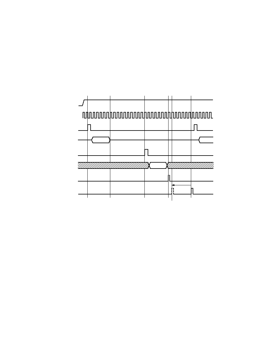
AD73311
34
REV. B
APPENDIX E
DAC Timing Control Example
The AD73311's DAC is loaded from the DAC register contents
just before the ADC register contents are loaded to the serial
register (SDOFS going high). This default DAC load position
can be advanced in time to occur earlier with respect to the
SDOFS going high. Figure 37 shows an example of the ADC
unload and DAC load sequence. At time t
1
the SDOFS is raised
to indicate that a new ADC word is ready. Following the SDOFS
pulse, 16 bits of ADC data are clocked out on SDO in the sub-
sequent 16 SCLK cycles finishing at time t
2
where the DSP's
SPORT will have received the 16-bit word. The DSP may
ADC WORD
DAC WORD
SE
SCLK
SDOFS
SDO
SDIFS
SDI
DAC REGISTER
UPDATE
DAC LOAD
FROM DAC REGISTER
t
6
t
4
t
5
t
3
t
2
t
1
Figure 37. DAC Timing Control
process this information and generate a DAC word to be sent to
the AD73311. Time t
3
marks the beginning of the sequence of
sending the DAC word to the AD73311. This sequence ends at
time t
4
where the DAC register will be updated from the 16 bits
in the AD73311's serial register. However, the DAC will not be
updated from the DAC register until time t
5
which may not be
acceptable in certain applications. In order to reduce this delay
and load the DAC at time t
6
, the DAC advance register can be
programmed with a suitable setting corresponding to the
required time advance (refer to Table VIII for details of DAC
Timing Control settings).

AD73311
35
REV. B
Topic
Page
FEATURES . . . . . . . . . . . . . . . . . . . . . . . . . . . . . . . . . . . . . 1
FUNCTIONAL BLOCK DIAGRAM . . . . . . . . . . . . . . . . . 1
GENERAL DESCRIPTION . . . . . . . . . . . . . . . . . . . . . . . . . 1
SPECIFICATIONS (3 V) . . . . . . . . . . . . . . . . . . . . . . . . . 2, 3
SPECIFICATIONS (5 V) . . . . . . . . . . . . . . . . . . . . . . . . . 4, 5
TIMING CHARACTERISTICS (3 V) . . . . . . . . . . . . . . . . . 6
TIMING CHARACTERISTICS (5 V) . . . . . . . . . . . . . . . . . 7
Timing Diagrams . . . . . . . . . . . . . . . . . . . . . . . . . . . . . . 7, 8
Performance Graphs . . . . . . . . . . . . . . . . . . . . . . . 8, 2224
ABSOLUTE MAXIMUM RATINGS . . . . . . . . . . . . . . . . . 9
ORDERING GUIDE . . . . . . . . . . . . . . . . . . . . . . . . . . . . . . 9
PIN CONFIGURATION . . . . . . . . . . . . . . . . . . . . . . . . . . . 9
PIN FUNCTION DESCRIPTIONS . . . . . . . . . . . . . . . . . 10
TERMINOLOGY . . . . . . . . . . . . . . . . . . . . . . . . . . . . . . . . 11
ABBREVIATIONS . . . . . . . . . . . . . . . . . . . . . . . . . . . . . . . 11
FUNCTIONAL DESCRIPTION . . . . . . . . . . . . . . . . . . . . 12
Encoder Channel . . . . . . . . . . . . . . . . . . . . . . . . . . . . . . . 12
Programmable Gain Amplifier . . . . . . . . . . . . . . . . . . . . . 12
ADC . . . . . . . . . . . . . . . . . . . . . . . . . . . . . . . . . . . . . . . . 12
Analog Sigma-Delta Modulator . . . . . . . . . . . . . . . . . . . . 12
Decimation Filter . . . . . . . . . . . . . . . . . . . . . . . . . . . . . . . 13
ADC Coding . . . . . . . . . . . . . . . . . . . . . . . . . . . . . . . . . . 13
Decoder Channel . . . . . . . . . . . . . . . . . . . . . . . . . . . . . . . 13
DAC Coding . . . . . . . . . . . . . . . . . . . . . . . . . . . . . . . . . . 13
Interpolation Filter . . . . . . . . . . . . . . . . . . . . . . . . . . . . . . 13
Analog Smoothing Filter & PGA . . . . . . . . . . . . . . . . . . . 14
Differential Output Amplifiers . . . . . . . . . . . . . . . . . . . . . 14
Voltage Reference . . . . . . . . . . . . . . . . . . . . . . . . . . . . . . 14
Serial Port (SPORT) . . . . . . . . . . . . . . . . . . . . . . . . . . . . 14
SPORT Overview . . . . . . . . . . . . . . . . . . . . . . . . . . . . . . . 14
SPORT Register Maps . . . . . . . . . . . . . . . . . . . . . . . . . . . 15
Master Clock Divider . . . . . . . . . . . . . . . . . . . . . . . . . . . . 15
Serial Clock Rate Divider . . . . . . . . . . . . . . . . . . . . . . . . . 15
DAC Advance Register . . . . . . . . . . . . . . . . . . . . . . . . . . 15
Topic
Page
OPERATION . . . . . . . . . . . . . . . . . . . . . . . . . . . . . . . . . . . 16
Resetting the AD73311 . . . . . . . . . . . . . . . . . . . . . . . . . . 16
Power Management . . . . . . . . . . . . . . . . . . . . . . . . . . . . . 16
Operating Modes . . . . . . . . . . . . . . . . . . . . . . . . . . . . . . . 16
Control Register Tables . . . . . . . . . . . . . . . . . . . . . . . 17, 18
Program (Control) Mode . . . . . . . . . . . . . . . . . . . . . . . . . 19
Data Mode . . . . . . . . . . . . . . . . . . . . . . . . . . . . . . . . . . . . 19
Mixed Program/Data Mode . . . . . . . . . . . . . . . . . . . . . . . 19
Analog Loop-Back . . . . . . . . . . . . . . . . . . . . . . . . . . . . . . 19
Digital Loop-Back . . . . . . . . . . . . . . . . . . . . . . . . . . . . . . 19
Interface Signal Timing . . . . . . . . . . . . . . . . . . . . . . . . . . 20
INTERFACING . . . . . . . . . . . . . . . . . . . . . . . . . . . . . . . . . 21
Cascade Operation . . . . . . . . . . . . . . . . . . . . . . . . . . . . . . 21
PERFORMANCE . . . . . . . . . . . . . . . . . . . . . . . . . . . . . . . . 22
Encoder Section . . . . . . . . . . . . . . . . . . . . . . . . . . . . . . . . 22
Encoder Group Delay . . . . . . . . . . . . . . . . . . . . . . . . . . . 23
Decoder Section . . . . . . . . . . . . . . . . . . . . . . . . . . . . . . . . 23
Decoder Group Delay . . . . . . . . . . . . . . . . . . . . . . . . . . . 24
DESIGN CONSIDERATIONS . . . . . . . . . . . . . . . . . . . . . 24
Analog Input . . . . . . . . . . . . . . . . . . . . . . . . . . . . . . . . . . 24
Analog Output . . . . . . . . . . . . . . . . . . . . . . . . . . . . . . . . . 25
Digital Interfacing . . . . . . . . . . . . . . . . . . . . . . . . . . . . . . 25
Cascade Operation . . . . . . . . . . . . . . . . . . . . . . . . . . . . . . 26
Grounding and Layout . . . . . . . . . . . . . . . . . . . . . . . . . . . 26
DSP Programming Considerations . . . . . . . . . . . . . . . . . 27
DSP SPORT Configuration . . . . . . . . . . . . . . . . . . . . . . . 27
DSP SPORT Interrupts . . . . . . . . . . . . . . . . . . . . . . . . . . 27
APPENDIX A (Single Device Data Mode Operation) . . . . . . 28
APPENDIX B (Single Device Mixed Mode Operation) . . . . . 29
APPENDIX C (Dual Device Data Mode Operation) . . . 30, 31
APPENDIX D (Dual Device Mixed Mode Operation) . . 32, 33
APPENDIX E (DAC Timing Control Example) . . . . . . . . . . 34
OUTLINE DIMENSIONS . . . . . . . . . . . . . . . . . . . . . . . . . 36
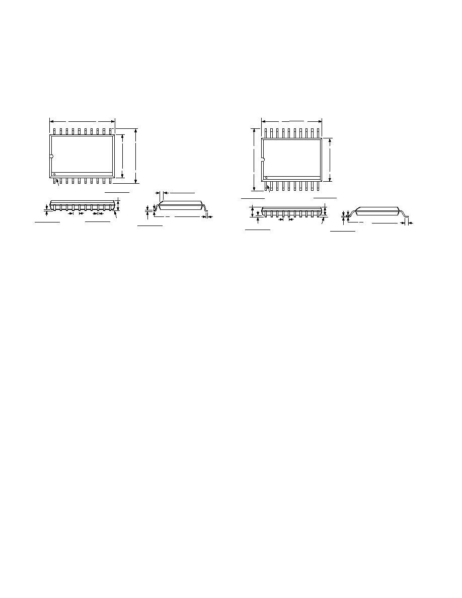
36
C00688a06/00 (rev. B)
PRINTED IN U.S.A.
AD73311
REV. B
20-Lead Small Outline IC
(R-20)
SEATING
PLANE
0.0118 (0.30)
0.0040 (0.10)
0.0192 (0.49)
0.0138 (0.35)
0.1043 (2.65)
0.0926 (2.35)
0.0500
(1.27)
BSC
0.0125 (0.32)
0.0091 (0.23)
0.0500 (1.27)
0.0157 (0.40)
8
0
0.0291 (0.74)
0.0098 (0.25)
45
20
11
10
1
0.5118 (13.00)
0.4961 (12.60)
0.4193 (10.65)
0.3937 (10.00)
0.2992 (7.60)
0.2914 (7.40)
PIN 1
20-Lead Shrink Small Outline IC
(RS-20)
20
11
10
1
0.295 (7.50)
0.271 (6.90)
0.311 (7.9)
0.301 (7.64)
0.212 (5.38)
0.205 (5.21)
PIN 1
SEATING
PLANE
0.008 (0.203)
0.002 (0.050)
0.07 (1.78)
0.066 (1.67)
0.0256
(0.65)
BSC
0.078 (1.98)
0.068 (1.73)
0.009 (0.229)
0.005 (0.127)
0.037 (0.94)
0.022 (0.559)
8
0
OUTLINE DIMENSIONS
Dimensions shown in inches and (mm).