Äîêóìåíòàöèÿ è îïèñàíèÿ www.docs.chipfind.ru
REV. 0
Information furnished by Analog Devices is believed to be accurate and
reliable. However, no responsibility is assumed by Analog Devices for its
use, nor for any infringements of patents or other rights of third parties
which may result from its use. No license is granted by implication or
otherwise under any patent or patent rights of Analog Devices.
a
AD6600
One Technology Way, P.O. Box 9106, Norwood, MA 02062-9106, U.S.A.
Tel: 781/329-4700
World Wide Web Site: http://www.analog.com
Fax: 781/326-8703
© Analog Devices, Inc., 2000
FUNCTIONAL BLOCK DIAGRAM
FEATURES
Dual IF Inputs, 70 MHz250 MHz
Diversity or Two Independent IF Signals
Separate Attenuation Paths
Oversample RF Channels
20 MSPS on a Single Carrier
10 MSPS/Channel in Diversity Mode
Total Signal Range 90+ dB
30 dB from Automatic Gain-Ranging (AGC)
60 dB from A/D Converter
Range >100 dB After Processing Gain
Digital Outputs
11-Bit ADC Word
3-Bit RSSI Word
2 Clock, A/B Indicator
Single 5 V Power Supply
Output DVCC 3.3 V or 5 V
775 mW Power Dissipation
APPLICATIONS
Communications Receivers
PCS/Cellular Base Stations
GSM, CDMA, TDMA
Wireless Local Loop, Fixed Access
PRODUCT DESCRIPTION
The AD6600 mixed-signal receiver chip directly samples signals
at analog input frequencies up to 250 MHz. The device includes
two input channels, each with 1 GHz input amplifiers and
30 dB of automatic gain-ranging circuitry. Both channels are
sampled with a 450 MHz track-and-hold followed by an 11-bit,
20 MSPS analog-to-digital converter. Digital RSSI outputs, an
A/B channel indicator, a 2
× Clock output, references, and con-
trol circuitry are all on-chip. Digital output signals are two's
complement, CMOS-compatible and interface directly to
3.3 V or 5 V digital processing chips.
The primary use for the dual analog input structure is sampling
both antennas in a two-antenna diversity receiver. However,
Channels A and B may also be used to sample two independent
IF signals. Diversity, or dual-channel mode, is limited to 10 MSPS
per channel. In single-channel mode, the full clock rate of
20 MSPS may be applied to a single carrier.
The AD6600 may be used as a stand-alone sampling chip, or it
may be combined with the AD6620 Digital Receive Signal Pro-
cessor. The AD6620 provides 10 dB25 dB of additional pro-
cessing gain before passing data to a fixed- or floating-point DSP.
Driving the AD6600 is simplified by using the AD6630 differen-
tial IF amplifier. The AD6630 is easily matched to inexpensive
SAW filters from 70 MHz to 250 MHz.
Designed specifically for cellular/PCS receivers, the AD6600
supports GSM, IS-136, CDMA and Wireless LANs, as well as
proprietary air interfaces used in WLL/fixed-access systems.
Units are available in plastic, surface-mount packages (44-lead
LQFP) and specified over the industrial temperature range
(40
°C to +85°C).
Dual Channel, Gain-Ranging
ADC with RSSI
GAIN
A/D
CONVERTER
TIMING
ENCODE
SELECT GAIN
+12, +18dB
ENCODE
FLT
FLT
NOISE FILTER
RESONANT
PORT
630
RSSI
3
TWO'S
COMPLEMENT
11
AB_OUT
D10D0
RSSI [2:0]
CLK2
DVCC
ENC
ENC
GND
AVCC
B_SEL
A_SEL
ANALOG MUX
GAIN
GAIN
RSSI
3
0dB, 12dB, 24dB
ATTEN
ATTEN
0dB, 12dB, 24dB
DETECT
PEAK
SET
RSSI
AIN
AIN
BIN
BIN
AD6600

REV. 0
2
AD6600SPECIFICATIONS
DC SPECIFICATIONS
Test
AD6600AST
Parameter
Temp
Level
Min
Typ
Max
Unit
ANALOG INPUTS (AIN,
AIN/BIN, BIN)
Differential Analog Input Voltage Range
1
Full
V
2.0
V p-p
Differential Analog Input Resistance
2
Full
IV
160
200
240
Differential Analog Input Capacitance
25
°C
V
1.5
pF
PEAK DETECTOR (Internal), RSSI
Resolution
3
Bits
RSSI Gain Step
Full
V
6
dB
RSSI Hysteresis
3
Full
V
6
dB
RESONANT PORT (FLT,
FLT)
Differential Port Resistance
Full
V
630
Differential Port Capacitance
Full
V
1.75
pF
A/D CONVERTER
Resolution
Full
IV
11
Bits
ENCODE INPUTS (ENC,
ENC)
Differential Input Voltage (AC-Coupled)
4
Full
IV
0.4
V p-p
Differential Input Resistance
25
°C
V
11
k
Differential Input Capacitance
25
°C
V
2.5
pF
A/B MODE INPUTS (A_SEL, B_SEL)
5
Input High Voltage Range
Full
IV
4.75
5.25
V
Input Low Voltage Range
Full
IV
0.0
0.5
V
POWER SUPPLY
Supply Voltages
AVCC
Full
II
4.75
5.0
5.25
V
DVCC
Full
IV
3.0
3.3
5.25
V
Supply Current
I
AVCC
(AVCC = 5.0 V)
Full
II
145
182
mA
I
DVCC
(DVCC = 3.3 V)
Full
II
15
20
mA
POWER CONSUMPTION
6
Full
II
775
976
mW
NOTES
1
Analog Input Range is a function of input frequency. See ac specifications for 70 MHz250 MHz inputs.
2
Analog Input Impedance is a function of input frequency. See ac specifications for 70 MHz450 MHz inputs.
3
Six dB of digital hysteresis is used to eliminate level uncertainty at the RSSI threshold points due to noise and amplitude variations.
4
Encode inputs should be ac-coupled and driven differentially. See Encoding the AD6600 for details.
5
A_SEL and B_SEL should be tied directly to ground or AVCC.
6
Maximum power consumption is computed as maximum current at nominal supplies.
Specifications subject to change without notice.
DIGITAL SPECIFICATIONS
Test
AD6600AST
Parameter
Temp
Level
Min
Typ
Max
Unit
LOGIC OUTPUTS (D10D0, AB_OUT, RSSI20)
1
Logic Compatibility
CMOS
Logic "1" Voltage (DVCC = 3.3 V)
Full
II
2.8
DVCC 0.2
V
Logic "0" Voltage (DVCC = 3.3 V)
Full
II
0.2
0.5
V
Logic "1" Voltage (DVCC = 5.0 V)
Full
IV
4.0
DVCC 0.35
V
Logic "0" Voltage (DVCC = 5.0 V)
Full
IV
0.35
0.5
V
Output Coding (D10D0)
Two's Complement
CLK2
× OUTPUT
1, 2
Logic "1" Voltage (DVCC = 3.3 V)
Full
II
2.8
DVCC 0.2
V
Logic "0" Voltage (DVCC = 3.3 V)
Full
II
0.2
0.5
V
Logic "1" Voltage (DVCC = 5.0 V)
Full
IV
4.0
DVCC 0.3
V
Logic "0" Voltage (DVCC = 5.0 V)
Full
IV
0.35
0.5
V
NOTES
1
Digital output load is one LCX gate.
2
CLK2
× output voltage levels, high and low, tested at switching rate of 10 MHz.
Specifications subject to change without notice.
(AVCC = 5 V, DVCC = 3.3 V; T
MIN
= 40 C, T
MAX
= +85 C unless otherwise noted.)
(AVCC = 5 V, DVCC = 3.3 V; T
MIN
= 40 C, T
MAX
= +85 C unless otherwise noted.)

REV. 0
3
AD6600
TIMING REQUIREMENTS AND SWITCHING SPECIFICATIONS
1
(AVCC = 5 V, DVCC = 3.3 V; ENC and
ENC = 20 MSPS; T
MIN
= 40 C, T
MAX
= +85 C unless otherwise noted.)
Test
AD6600AST
Parameter
Name
Temp
Level
Min
Typ
Max
Unit
A/D CONVERTER
Conversion Rate
f
ENC
1/(t
ENC
)
MSPS
Maximum Conversion Rate
Full
II
20
MSPS
Minimum Conversion Rate
Full
IV
6
MSPS
Aperture Uncertainty
t
j
25
°C
V
0.3
ps rms
ENCODE INPUTS (ENC,
ENC)
2
Period
t
ENC
Full
II
50
ns
Pulsewidth High
3
t
ENCH
Full
IV
20
ns
Pulsewidth Low
4
t
ENCL
Full
IV
20
ns
2
× CLOCK OUTPUT (CLK2×)
5
Output Frequency
2
× f
ENC
MSPS
Output Period
6
t
CLK2
×_1
Full
V
t
ENCL
ns
t
CLK2
×_2
Full
V
t
ENCH
ns
CLK2
× Pulsewidth Low
6
t
CLK2
×L
Full
V
t
ENCH
/2
ns
Output Risetime
7
Full
V
3
ns
Output Falltime
7
Full
V
2.6
ns
OUTPUT RISE/FALL TIMES
8
Output Risetime (D10:D0, RSSI2:0)
Full
V
8
ns
Output Falltime (D10:D0, RSSI2:0)
Full
V
8.4
ns
Output Risetime (AB_OUT)
Full
V
6
ns
Output Falltime (AB_OUT)
Full
V
6.2
ns
NOTES
1
See AD6600 Timing Diagrams.
2
All switching specifications tested by driving ENC and
ENC differentially.
3
Several timing specifications are a function of Encode high time, t
ENCH
; these specifications are shown in the data tables and timing diagrams. Encode duty cycle
should be kept as close to 50% as possible.
4
Encode pulse low directly affects the amount of settling time available at FLT resonant port. See External Analog (Resonant) Filter section for details.
5
The 2
× Clock is generated internally, therefore some specifications are functions of encode period and duty cycle. All timing measurements to or from CLK2 × are
referenced to 2.0 V crossing.
6
This specification IS a function of Encode period and duty cycle; reference timing diagrams Figure 8.
7
Output rise time is measured from 20% point to 80% point of total CLK2
× voltage swing; output fall time is measured from 80% point to 20% point of total CLK2×
voltage swing.
8
Output rise time is measured from 20% point to 80% point of total data voltage swing; output fall time is measured from 80% point to 20% point of total data voltage
swing. All outputs specified with 10 pF load.
Specifications subject to change without notice.

REV. 0
4
AD6600SPECIFICATIONS
TIMING REQUIREMENTS AND SWITCHING SPECIFICATIONS
1, 2
(AVCC = 5 V, DVCC = 3.3 V; ENC and
ENC = 20 MSPS, Duty Cycle = 50%; T
MIN
= 40 C, T
MAX
= +85 C unless otherwise noted.)
Test
AD6600AST
Parameter
Name
Temp
Level
Min
Typ
Max
Unit
ENCODE/CLK2
×
Encode Rising to CLK2
× Falling
3
t
CF
Full
IV
6.5
8.0
9.5
ns
Encode Rising to CLK2
× Rising
4
t
CR
Full
IV
t
CF
+ (t
ENCH
)/2
ns
@ Encode = 13 MSPS, 50% Duty Cycle
Full
IV
25.7
27.2
28.7
ns
@ Encode = 20 MSPS, 50% Duty Cycle
Full
IV
19.0
20.5
22.0
ns
CLK2
×/DATA (D10:0, RSSI2:0)
5
CLK2
× to DATA Rising Low Delay
3
t
2
×_DRL
Full
IV
3.0
6.5
ns
CLK2
× to DATA Hold Time
3
t
H_D2
×
Full
IV
3.0
6.5
ns
CLK2
× to DATA Falling Low
3, 6
t
2
×_DFL
25
°C
IV
10.0
15.0
20.0
ns
Full
IV
11.0
15.5
22.0
ns
CLK2
× to DATA Setup Time
4
t
S_D2
×
Full
IV
t
ENCH
t
2
×_DFL
ns
@ Encode = 13 MSPS, 50% Duty Cycle
Full
IV
16.5
23.0
ns
@ Encode = 20 MSPS, 50% Duty Cycle
6
25
°C
IV
5.0
10.0
ns
Full
IV
3.0
9.5
ns
CLK2
×/AB_OUT
5
CLK2
× to AB_OUT Rising Low Delay
3
t
2
×_ARL
Full
IV
7.0
11.0
ns
CLK2
× to AB_OUT Hold Time
3
t
H_A2
×
Full
IV
7.0
11.0
ns
CLK2
× to AB_OUT Falling Low Delay
3, 6
t
2
×_AFL
25
°C
IV
12.0
18.0
23.0
ns
Full
IV
10.7
19.0
26.0
ns
CLK2
× to AB_OUT Setup Time
4
t
S_A2
×
Full
IV
t
ENCH
t
2
×_AFL
ns
@ Encode = 13 MSPS, 50% Duty Cycle
Full
IV
12.5
19.5
ns
@ Encode = 20 MSPS, 50% Duty Cycle
6
25
°C
IV
2.0
7.0
ns
Full
IV
1.0
6.0
ns
ENCODE/DATA (D10:0, RSSI2:0)
ENCODE to DATA Rising Low Delay
4
t
EN_DRL
Full
IV
t
CR
+ t
2
×_DRL
ns
ENCODE to DATA Hold Time
4
t
H_DEN
Full
IV
t
EN_DRL
ns
@ Encode = 13 MSPS, 50% Duty Cycle
Full
IV
28.7
33.7
ns
@ Encode = 20 MSPS, 50% Duty Cycle
Full
IV
22.0
27.0
ns
ENCODE to DATA Falling Low Delay
4
t
EN_DFL
Full
IV
t
CR
+ t
2
×_DFL
ns
ENCODE to DATA Delay (Setup)
4
t
S_DEN
Full
IV
t
ENC
t
EN_DFL
ns
@ Encode = 13 MSPS, 50% Duty Cycle
Full
IV
26.2
34.2
ns
@ Encode = 20 MSPS, 50% Duty Cycle
6
25
°C
IV
8.0
14.5
ns
Full
IV
6.0
14.0
ns
ENCODE/AB_OUT
ENCODE to AB_OUT Rising Low Delay
4
t
EN_ARL
Full
IV
t
CR
+ t
2
×_ARL
ns
ENCODE to AB_OUT Delay (Hold)
4
t
H_AEN
Full
IV
t
EN_ARL
ns
@ Encode = 13 MSPS, 50% Duty Cycle
Full
IV
32.7
38.2
ns
@ Encode = 20 MSPS, 50% Duty Cycle
Full
IV
26.0
31.5
ns
ENCODE to AB_OUT Falling Low Delay
4
t
EN_AFL
Full
IV
t
CR
+ t
2
×_AFL
ns
ENCODE to AB_OUT Delay (Setup)
4
t
S_AEN
Full
IV
t
ENC
t
EN_AFL
ns
@ Encode = 13 MSPS, 50% Duty Cycle
Full
IV
22.2
30.7
ns
@ Encode = 20 MSPS, 50% Duty Cycle
6
25
°C
IV
5.0
11.5
ns
Full
IV
2.0
10.5
ns
NOTES
1
See AD6600 Timing Diagrams.
2
All switching specifications tested by driving ENC and
ENC differentially.
3
This specification IS NOT a function of Encode period and duty cycle.
4
This specification IS a function of Encode period and duty cycle.
5
CLK2
× referenced to 2.0 V crossing; digital output levels referenced to 0.8 V and 2.0 V crossings; all outputs with 10 pF load.
6
For these particular specifications, the 25
°C specification is valid from 25°C to 85°C. The Full temperature specification includes cold temperature extreme and
covers the entire range, 40
°C to +85°C.
Specifications subject to change without notice.

REV. 0
5
AD6600
AC SPECIFICATIONS
Test
AD6600AST
Parameter
Temp
Level
Min
Typ
Max
Unit
ANALOG INPUTS
1
Analog Input 3 dB Bandwidth
2
Full
V
450
MHz
Differential Analog Input Voltage Range
70 MHz
Full
V
2.45
V p-p
150 MHz
Full
V
2.57
V p-p
200 MHz
Full
V
2.62
V p-p
250 MHz
Full
V
2.86
V p-p
Differential Analog Input Impedance
3
70 MHz
25
°C
V
197j24
150 MHz
25
°C
V
188j48
200 MHz
25
°C
V
175j57
250 MHz
25
°C
V
161j67
300 MHz
25
°C
V
151j73
350 MHz
25
°C
V
140j80
400 MHz
25
°C
V
141j75
450 MHz
25
°C
V
173j107
Full-Scale Input Power
70 MHz
Full
V
5.8
dBm
150 MHz
Full
V
6.3
dBm
200 MHz
Full
V
6.7
dBm
250 MHz
Full
V
7.7
dBm
Full-Scale Gain Tolerance
4
70 MHz250 MHz
Full
V
±0.5
dB
200 MHz
5
25
°C
I
1.0
±0.1
+1.0
dB
Gain Error
AIN = 200 MHz
@ 76 dBFS
25
°C
I
1.5
+1.5
dB
Gain Matching (Input A:B)
70 MHz250 MHz
Full
V
±0.1
dB
200 MHz
Full
II
0.5
±0.05
+0.5
dB
Range-to-Range Gain Tolerance
70 MHz250 MHz
Full
V
±0.1
dB
Range-to-Range Phase Tolerance
70 MHz
Full
V
0.2
Degree
250 MHz
Full
V
0.5
Degree
Channel Isolation
6
70 MHz250 MHz
Full
IV
45
50
dB
Noise
7
Minimum Attenuation Level
Full
V
34
µV rms
Maximum Attenuation Level
Full
V
869
µV rms
Attenuator 3OIP
8
Full
V
+33
dBm
Signal-to-Noise Ratio (SNR)
9, 10, 11
AIN = 70 MHz
@ 1 dBFS
25
°C
IV
55
59
dB
@ 6 dBFS
25
°C
V
54.5
dB
@ 10 dBFS
25
°C
IV
45
49
dB
@ 12 dBFS to 42 dBFS
25
°C
IV
41
48
±6
dB
@ 54 dBFS
25
°C
IV
31
34
dB
AIN = 150 MHz
@ 1 dBFS
25
°C
IV
55
58
dB
@ 6 dBFS
25
°C
V
54
dB
@ 10 dBFS
25
°C
IV
45
49
dB
@ 12 dBFS to 42 dBFS
25
°C
IV
41
48
±6
dB
@ 54 dBFS
25
°C
IV
31
34
dB
(AVCC = 5 V, DVCC = 3.3 V; ENC and
ENC = 20 MSPS, Duty Cycle = 50%; T
MIN
= 40 C, T
MAX
= +85 C unless
otherwise noted.)

REV. 0
6
AD6600SPECIFICATIONS
AC SPECIFICATIONS (continued)
Test
AD6600AST
Parameter
Temp
Level
Min
Typ
Max
Unit
ANALOG INPUTS (Continued)
Signal-to-Noise Ratio (Continued)
AIN = 200 MHz
@ 1 dBFS
25
°C
I
55
57.5
dB
@ 6 dBFS
25
°C
V
53.5
dB
@ 10 dBFS
25
°C
I
45
49
dB
@ 12 dBFS to 42 dBFS
25
°C
I
40.5
48
±6
dB
@ 54 dBFS
25
°C
I
31
34
dB
AIN = 250 MHz
@ 1 dBFS
25
°C
IV
52
56
dB
@ 6 dBFS
25
°C
V
53.5
dB
@ 10 dBFS
25
°C
IV
43
49
dB
@ 12 dBFS to 42 dBFS
25
°C
IV
40
48
±6
dB
@ 54 dBFS
25
°C
IV
30
34
dB
SECOND HARMONIC
AIN = 70 MHz
@ 1 dBFS
Full
V
69
dBc
@ 6 dBFS
Full
V
68
dBc
@ 12 dBFS to 42 dBFS
Full
V
68
±6
dBc
AIN = 150 MHz
@ 1 dBFS
Full
V
60
dBc
@ 6 dBFS
Full
V
59
dBc
@ 12 dBFS to 42 dBFS
Full
V
67
±6
dBc
AIN = 200 MHz
9, 10, 11
@ 1 dBFS
25
°C
I
50
60
dBc
@ 6 dBFS
Full
V
56
dBc
@ 10 dBFS
25
°C
I
48
55
dBc
@ 12 dBFS to 42 dBFS
Full
V
65
±6
dBc
@ 54 dBFS
Full
V
50
dBc
AIN = 250 MHz
@ 1 dBFS
Full
V
54
dBc
@ 6 dBFS
Full
V
62
dBc
@ 12 dBFS to 42 dBFS
Full
V
65
±6
dBc
THIRD HARMONIC
AIN = 70 MHz
@ 1 dBFS
Full
V
77
dBc
@ 6 dBFS
Full
V
76
dBc
@ 12 dBFS to 42 dBFS
Full
V
67
±6
dBc
AIN = 150 MHz
@ 1 dBFS
Full
V
65
dBc
@ 6 dBFS
Full
V
70
dBc
@ 12 dBFS to 42 dBFS
Full
V
66
±6
dBc
AIN = 200 MHz
9, 10, 11
@ 1 dBFS
25
°C
I
50
55
dBc
@ 6 dBFS
Full
V
58
dBc
@ 10 dBFS
25
°C
I
55
66
dBc
@ 12 dBFS to 42 dBFS
Full
V
65
±6
dBc
@ 54 dBFS
Full
V
62
dBc
AIN = 250 MHz
@ 1 dBFS
Full
V
50
dBc
@ 6 dBFS
Full
V
56
dBc
@ 12 dBFS to 42 dBFS
Full
V
65
±6
dBc
AIN = 70 MHz250 MHz
@ 75 dBFS
Full
IV
28
35
dBc

REV. 0
7
AD6600
AC SPECIFICATIONS (continued)
Test
AD6600AST
Parameter
Temp
Level
Min
Typ
Max
Unit
WORST OTHER SPUR (4th or Higher)
AIN = 70 MHz
@ 1 dBFS
Full
V
74.5
dBc
@ 6 dBFS
Full
V
71
dBc
@ 12 dBFS to 42 dBFS
Full
V
68
±6
dBc
AIN = 150 MHz
@ 1 dBFS
Full
V
67
dBc
@ 6 dBFS
Full
V
65
dBc
@ 12 dBFS to 42 dBFS
Full
V
67
±6
dBc
AIN = 200 MHz
@ 1 dBFS
25
°C
I
60
67
dBc
@ 6 dBFS
Full
V
66
dBc
@ 10 dBFS
25
°C
I
55
66
dBc
@ 12 dBFS to 42 dBFS
Full
V
65
±6
dBc
AIN = 250 MHz
@ 1 dBFS
Full
V
66.5
dBc
@ 6 dBFS
Full
V
65
dBc
@ 12 dBFS to 42 dBFS
Full
V
65
±6
dBc
NOTES
1
AIN,
AIN/BIN, BIN: The AD6600 analog inputs are unconditionally stable and guarantee proper operation over the 70 MHz250 MHz specified operating range.
Circuit board layout is critical on this device, and proper PCB layout must be employed to achieve specified results.
2
Analog Input 3 dB Bandwidth is determined by internal track-and-hold. The front-end attenuators have a bandwidth of 1 GHz.
3
Measured real and imaginary values using Network Analyzer.
4
Full-scale gain tolerance is the typical variation in gain at a given IF input frequency. The nominal value for full-scale input power is a function of frequency as
shown in previous specification.
5
Full-scale gain tolerance measured at 200 MHz analog input referenced to 6.7 dBm nominal full-scale input power. For the gain measurement test, the input signal
level is set to 6 dBFS. Tuning port bandwidth is set to 50 MHz.
6
Main channel set to full-scale input power. Diversity channel swept from 20 dBFS to 90 dBFS.
7
Measurement includes thermal and quantization noise at 70 MHz analog input. Tuning port bandwidth is set to 50 MHz.
8
Test tones at 160.05 MHz and 170.05 MHz.
9
Measurements at 1 dFBS, 6 dBFS, and 10 dBFS are in highest attenuation mode, RSSI = 101.
10
Each gain-range is checked at ~3 dB from RSSI trip point (not in hysteresis); nominally 16 dBFS (RSSI = 100), 22 dBFS (RSSI = 011), 28 dBFS (RSSI = 010),
35 dBFS (RSSI = 001).
11
Measurement at 54 dBFS is in the lowest attenuation mode, RSSI = 000.
Specifications subject to change without notice.
REV. 0
AD6600
8
ABSOLUTE MAXIMUM RATINGS
1
Parameter
Min Max
Unit
ELECTRICAL
AVCC Voltage
0
7
V
DVCC Voltage
0
7
V
Analog Input Voltage
2
0
AVCC V
Analog Input Current
2
25
mA
Digital Input Voltage
3
0
AVCC V
Output Current
4
4
mA
Resonant Port Voltage
5
0
AVCC V
ENVIRONMENTAL
6
Operating Temperature Range
(Ambient)
40 +85
°C
Maximum Junction Temperature
150
°C
Lead Temperature (Soldering, 10 sec)
300
°C
Storage Temperature Range (Ambient)
65 +150
°C
NOTES
1
Absolute maximum ratings are limiting values to be applied individually, and
beyond which the serviceability of the circuit may be impaired. Functional
operability is not necessarily implied. Exposure to absolute maximum rating
conditions for an extended period of time may affect device reliability.
2
Pins AIN,
AIN, BIN, BIN.
3
Pins ENC,
ENC, A_SEL, B_SEL.
4
Pins D10:0, RSSI2:0, AB_OUT, CLK2
×.
5
Pins FLT,
FLT.
6
Typical thermal impedance (44-lead LQFP);
JC
= 16
°C/W,
JA
= 55
°C/W.
EXPLANATION OF TEST LEVELS
Test Level
I.
100% Production Tested.
II. 100% Production Tested at 25
°C and guaranteed by design
and characterization at temperature extremes.
IV. Parameter is guaranteed by design and characterization
testing.
V. Parameter is a typical value only.
ORDERING GUIDE
Temperature Package
Package
Model
Range
Description
Option
AD6600AST
40
°C to
44-Terminal LQFP ST-44
+85
°C
(Low-Profile Quad
(Ambient)
Plastic Flatpack)
AD6600ST/PCB
Evaluation Board
with AD6600AST
CAUTION
ESD (electrostatic discharge) sensitive device. Electrostatic charges as high as 4000 V readily
accumulate on the human body and test equipment and can discharge without detection. Although
the AD6600 features proprietary ESD protection circuitry, permanent damage may occur on devices
subjected to high-energy electrostatic discharges. Therefore, proper ESD precautions are recom-
mended to avoid performance degradation or loss of functionality.
WARNING!
ESD SENSITIVE DEVICE
REV. 0
9
AD6600
PIN FUNCTION DESCRIPTIONS
Pin Number
Name
Function
1, 33
DVCC
Digital VCC for Digital Outputs. Can be 3.3 V.
2, 5, 13, 19, 21, 24, 30, 32
GND
Ground.
3
C1
Internal Bias Point. Bypass by 0.01
µF to GND.
4, 14, 15, 18, 20, 25, 31
AVCC
5 V Power Supply.
68
RSSI[2:0]
RSSI Digital Output Bits.
9, 10
B_SEL, A_SEL
Mode Select Pins for Analog Input Channel A and B Sampling.
11
AIN
True Analog Input Channel A.
12
AIN
Complementary Analog Input Channel A.
16, 17
FLT, FLT
Resonant Filter Pins for External LC Noise Filter.
22
BIN
Complementary Analog Input Channel B.
23
BIN
True Analog Input Channel B.
26
ENC
Complementary Encode Input.
27
ENC
True Encode Input.
28
CLK2
×
2
× Clock Output Used for Clocking Digital Filter Chips.
29
AB_OUT
Digital Output Flag Indicating Whether Output Is Input A (High) or B (Low).
34
D0
Digital Data Output Bit (Least Significant Bit)
*.
3543
D1D9
Digital Data Output Bits
*.
44
D10
Digital Data Output Bit (Most Significant Bit)
*.
*Digital Outputs (D10:D0) in Two's Complement Format.
PIN CONFIGURATION
3
4
5
6
7
1
2
10
11
8
9
40 39 38
41
42
43
44
36 35 34
37
29
30
31
32
33
27
28
25
26
23
24
PIN 1
IDENTIFIER
TOP VIEW
(Not to Scale)
12 13 14 15 16 17 18 19 20 21 22
DVCC
GND
AVCC
GND
AB_OUT
CLK2
ENC
AD6600
ENC
AVCC
GND
BIN
GND
D10 (MSB)
D9
D8
D7
D6
D5
D4
D3
D2
D1
D0 (LSB)
AVCC
GND
BIN
FLT
AIN
GND
AVCC
AVCC
FLT
AVCC
DVCC
GND
C1
AVCC
GND
RSSI2
RSSI1
RSSI0
B_SEL
A_SEL
AIN

REV. 0
AD6600
10
DEFINITIONS OF SPECIFICATIONS
Analog Bandwidth
The analog input frequency at which the spectral power of the
fundamental frequency (as determined by the FFT analysis) is
reduced by 3 dB. The bandwidth is determined by the internal
track-and-hold when the filter node is resonated.
Aperture Delay
The delay between the 50% point of the rising edge of the
ENCODE command and the instant at which the analog input-
is sampled.
Aperture Uncertainty (Jitter)
The sample-to-sample variation in aperture delay.
Attenuator 3OIP
The third order intercept point of the front end of the AD6600.
It is the point at which the third order products would theoreti-
cally intercept the input signal level if the input level could increase
without bounds. This is measured using the ADC within the
AD6600 while the input is stimulated with dual tones in the
minimum attenuation (i.e., maximum gain) range.
Channel Isolation
The amount of signal leakage from one channel to the next
when one channel is driven with a full-scale input, and the other
channel is swept from 20 dBFS to 90 dBFS with a frequency
offset. The leakage is measured on the side with the smaller signal.
Differential Analog Input Resistance, Differential Analog
Input Capacitance and Differential Analog Input Impedance
The real and complex impedances measured at each analog
input port. The resistance is measured statically and the capaci-
tance and differential input impedances are measured with a
network analyzer.
Differential Analog Input Voltage Range
The peak-to-peak differential voltage that must be applied to the
converter to generate a full-scale response. Peak differential
voltage is computed by observing the voltage on a single pin and
subtracting the voltage from the other pin, which is 180 degrees
out of phase. Peak-to-peak differential is computed by rotating
the inputs phase 180 degrees and taking the peak measurement
again. The difference is then computed between both peak
measurements.
Differential Nonlinearity
The deviation of any code width from an ideal 1 LSB step.
Differential Resonant Port Resistance
The resistance shunted across the resonant port (nominally
630
). Used to determine the filter bandwidth and gain of
that stage.
Encode Pulsewidth/Duty Cycle
Pulsewidth high is the minimum amount of time that the
ENCODE pulse should be left in logic "1" state to achieve rated
performance; pulsewidth low is the minimum time ENCODE
pulse should be left in low state. See timing implications of
changing t
ENCH
in text. At a given clock rate, these specifications
define an acceptable Encode duty cycle.
Full-Scale Gain Tolerance
Unit-to-unit variation in full-scale input power.
Full-Scale Input Power
Expressed in dBm. Computed using the following equation:
Power
V
Z
FULL SCALE
FULL SCALE rms
INPUT
=
10
0 001
2
log
.
Gain Matching (Input A:B)
Variation in full-scale power between A and B inputs.
Harmonic Distortion, 2nd
The ratio of the rms signal amplitude to the rms value of the
second harmonic component, reported in dBc.
Harmonic Distortion, 3rd
The ratio of the rms signal amplitude to the rms value of the
third harmonic component, reported in dBc.
Integral Nonlinearity
The deviation of the transfer function from a reference line
measured in fractions of 1 LSB using a "best straight line"
determined by a least square curve fit.
Minimum Conversion Rate
The encode rate at which the SNR of the lowest analog signal fre-
quency drops by no more than 3 dB below the guaranteed limit.
Maximum Conversion Rate
The encode rate at which parametric testing is performed.
Noise (For Any Range Within the ADC)
V
Z
NOISE
FS
SNR
Signal
dBm
dBc
dBFS
=
×
×
-
-
0 001 10
10
.
where:
Z
is the input impedance,
FS
is the full-scale of the device for the frequency in question,
SNR is the value for the particular input level,
Signal is the signal level within the ADC reported in dB below
full scale. This value includes both thermal and quanti-
zation noise.
Range-Range Gain Tolerance
The gain error in the RSSI attenuator ladder from one range to
the next.
Range-Range Phase Tolerance
The phase error in the RSSI attenuator ladder from one range
to the next.
Differential Resonant Port Capacitance
The capacitance between the two resonant pins. Used to deter-
mine filter bandwidth and resonant frequency.
REV. 0
AD6600
11
RSSI Gain Step
The input amplitude span between taps of the RSSI (received
signal strength) attenuator ladder. Ideally each stage should
span 6 dB of input power.
RSSI Hysteresis
The amount of movement in the RSSI switch points, depending
on the direction of approach. Hysteresis prevents unnecessary
RSSI toggling when input signal power is near a threshold.
Signal-to-Noise Ratio (Without Harmonics)
The ratio of the rms signal amplitude (set at 1 dB below full
scale) to the rms value of the sum of all other spectral compo-
nents, excluding the first five harmonics and dc.
Worst Other Spur
The ratio of the rms signal amplitude to the rms value of the
worst spurious component (excluding the second and third
harmonic) reported in dBc.
AD6600 TRANSFER FUNCTION
AIN LEVEL dBFS
60
24
0
100
0
90
SNR
dB
80
70
60
50
40
30
20
10
54
30
18
6
42
36
12
48
Figure 1. SNR vs. Input Power
REV. 0
AD6600
12
EQUIVALENT CIRCUITS
100
100
ATTENUATOR STAGE
EQUIVALENT INPUT R
SHOWN ONLY
AVCC
AVCC
GND
GND
V
REF
AIN
AIN
4 /8 GAIN STAGE
BUF
GAIN
BUF
Figure 2. Analog Input Stage (Channel A Shown;
Channel B Is Equivalent)
AVCC
GND
GND
AVCC
BIAS
AVCC
GND
B_SEL
ISEL_A
ISEL_B
A_SEL
Figure 3. A_SEL, B_SEL Input Mode Pins
DVCC
CURRENT
MIRROR
DVCC
CURRENT
MIRROR
V
REF
D10D0
RSSI [2:0]
500
Figure 4. Digital Outputs
315
315
AVCC
GND
AVCC
GND
AVCC
GND
FROM
GAIN STAGE
TO T/H
EXTERNAL LC FILTER
FLT
FLT
Figure 5. Resonant (LC Noise Filter) Port
R1
17k
1/2
R1
17k
1/2
R2
8k
1/2
R2
8k
1/2
AVCC
ENCODE
ENCODE
AVCC
TIMING
CIRCUITS
AVCC
Figure 6. Encode Inputs
DVCC
CURRENT
MIRROR
DVCC
CURRENT
MIRROR
V
REF
CLK2
AB_OUT
Figure 7. CLK2 , AB_OUT Outputs
REV. 0
AD6600
13
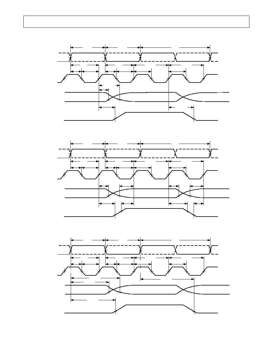
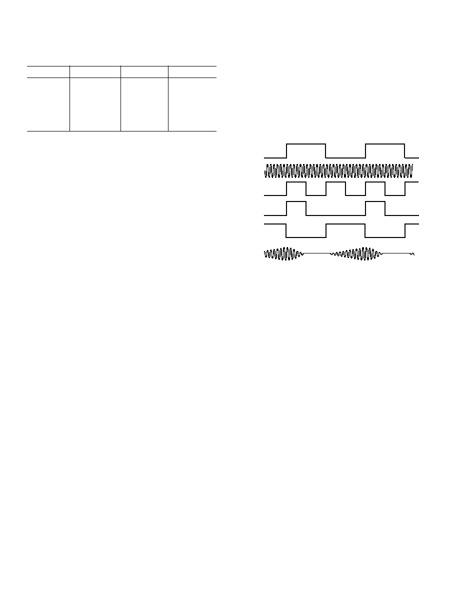
AD6600 TIMING DIAGRAMS
ENCODE
CLK2
D [10:0]
RSSI [2:0]
AB_OUT
t
CLK2 H1
t
CLK2 H2
t
CLK2 L
t
CF2
t
CLK2 L
t
CF1
CLK2 2
CLK2 1
CLK2 2
CLK2 1
CLK2 2
t
2 1_DRL
t
2 1_ARL
t
ENCH
t
ENCL
t
ENC
t
CLK2 1
t
CLK2 2
t
CR2
t
CR1
t
2 1_DFL
t
2 1_AFL
Figure 8. Encode to CLK2 Delays and CLK2 Propagation Delays
ENCODE
CLK2
D [10:0]
RSSI [2:0]
AB_OUT
t
CLK2 H1
t
CLK2 H2
t
CLK2 L
t
CF2
t
CLK2 L
t
CF1
CLK2 2
CLK2 1
CLK2 2
CLK2 1
CLK2 2
t
H_D2
t
ENCH
t
ENCL
t
ENC
t
CLK2 1
t
CLK2 2
t
CR2
t
CR1
t
S_D2
t
H_D2
t
S_D2
t
H_A2
t
S_A2
t
H_A2
t
S_A2
Figure 9. CLK2 Setup-and-Hold Time Characteristics
ENCODE
CLK2
D [10:0]
RSSI [2:0]
AB_OUT
t
CLK2 H1
t
CLK2 H2
t
CLK2 L
t
CF2
t
CLK2 L
t
CF1
CLK2 2
CLK2 1
CLK2 2
CLK2 1
CLK2 2
t
ENCH
t
ENCL
t
ENC
t
CLK2 1
t
CLK2 2
t
CR2
t
CR1
t
EN_DFL
t
EN_AFL
ENCODE
ENCODE
ENCODE
t
EN_ARL
t
EN_DRL
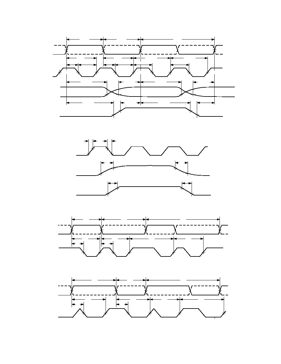
Figure 10. Encode to CLK2 Delays and Encode Propagation Delays
REV. 0
AD6600
14
ENCODE
CLK2
D [10:0]
RSSI [2:0]
AB_OUT
t
CLK2 H1
t
CLK2 H2
t
CLK2 L
t
CF2
t
CLK2 L
t
CF1
CLK2 2
CLK2 1
CLK2 2
CLK2 1
CLK2 2
t
ENCH
t
ENCL
t
ENC
t
CLK2 1
t
CLK2 2
t
CR2
t
CR1
t
S_DEN
t
H_DEN
t
S_DEN
t
H_DEN
t
H_AEN
t
S_AEN
t
H_AEN
t
S_AEN
ENCODE
ENCODE
ENCODE
Figure 11. Encode Setup-and-Hold Time Characteristics
CLK2
D [10:0]
RSSI [2:0]
AB_OUT
3
2.6
8
8.4
6.2
6
Figure 12. Typical Output Rise and Fall Times
ENCODE
CLK2
20
30
50
20
30
18
18
8
8
40%
Figure 13. Encode = 20 MSPS, Duty Cycle = 40%
ENCODE
CLK2
20
30
50
20
30
8
8
60%
23
23
Figure 14. Encode = 20 MSPS, Duty Cycle = 60%
REV. 0
AD6600
15
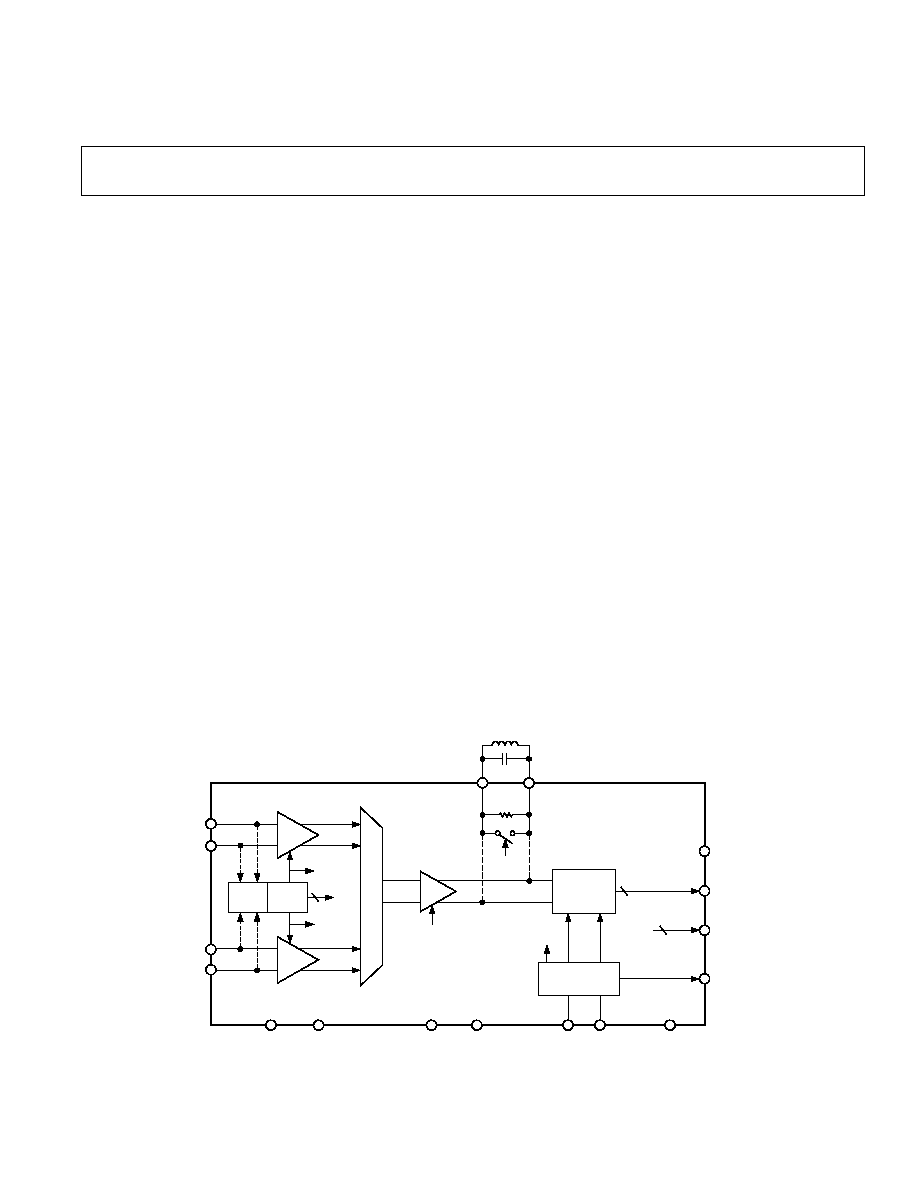
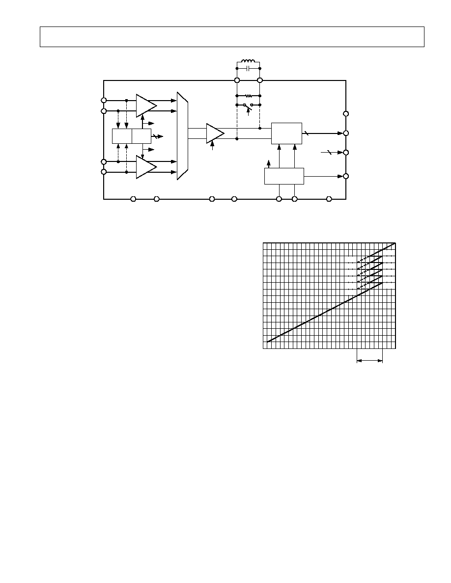
THEORY OF OPERATION
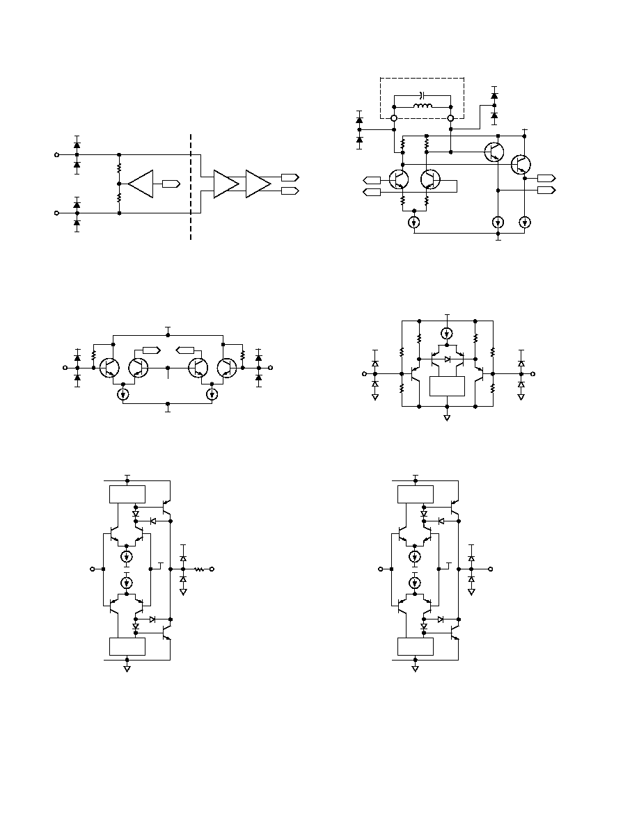
The AD6600, dual-channel, gain-ranging ADC integrates ana-
log IF circuitry with high speed data conversion. Each analog
input stage is a 1 GHz, 0 dB to 24 dB, phase-compensated step
attenuator; the step size in each attenuator is 12 dB. Both input
stages drive an analog multiplex function followed by a 12 dB/
18 dB gain amplifier. A simple LC noise filter at the output of
the gain amplifier is required to resonate at the desired IF. This
resonant filter port precedes a wide input bandwidth (450 MHz)
track-and-hold followed by an 11-bit analog-to-digital converter
(ADC). A high speed synchronous peak detector monitors sig-
nal strength at both input channels. The peak detector drives
RSSI circuitry that automatically adjusts attenuation and gain
on a clock-by-clock basis. The three RSSI indicator bits and the
eleven ADC bits are available at the output providing an exponent
and mantissa data format. Together these integrated components
form an IF sampling, high dynamic range ADC system.
It is helpful to view this device as a stand-alone ADC using
automatic gain control. The gain control referred to in this data
sheet as "gain-ranging" works to maintain a constant SNR over
as wide a range as possible.
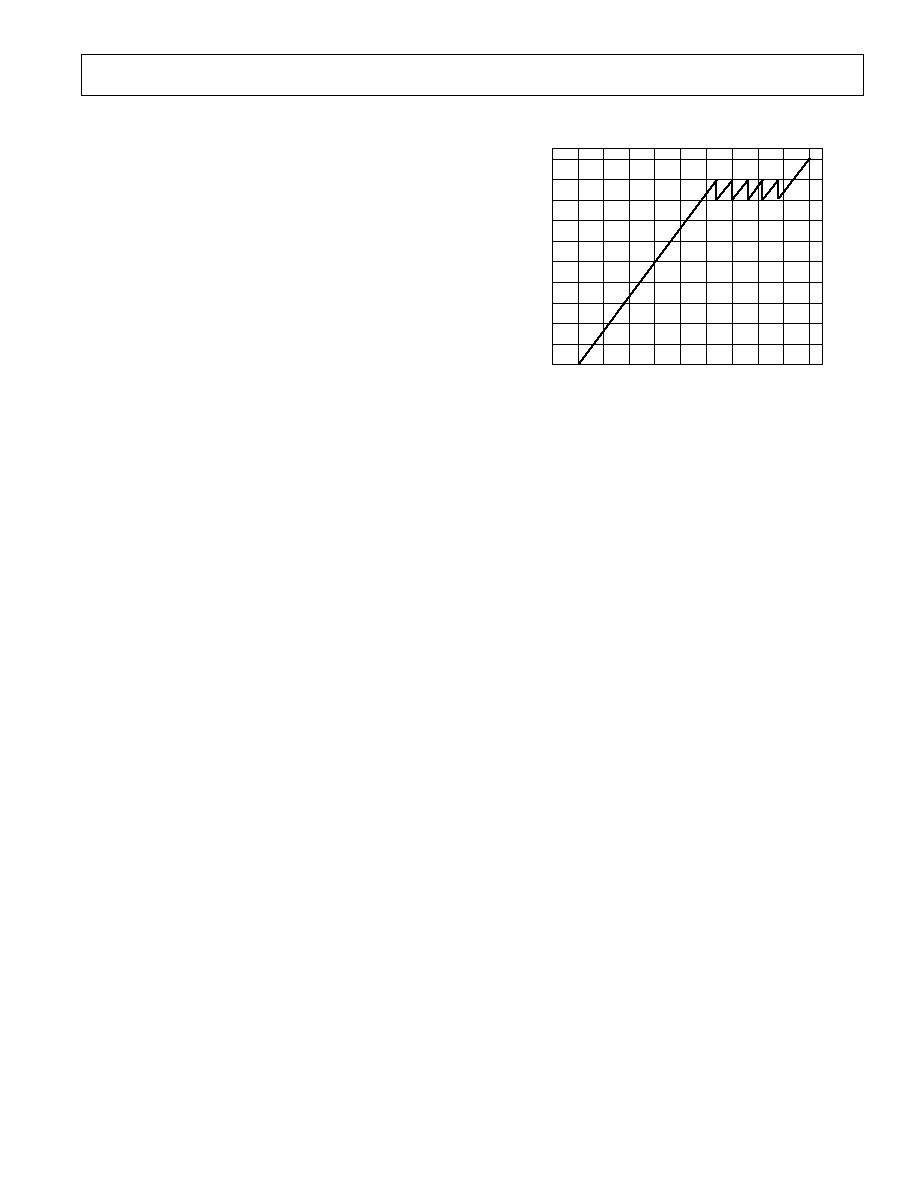
As stated previously, the AD6600 has a floating-point output:
eleven mantissa bits and three exponent bits. As shown in Fig-
ure 16, at the lowest input levels SNR increases 1 dB for a 1 dB
increase in input power. In this range, the AD6600 is set for
maximum gain. However, when the input signal level reaches
the gain-ranging section (approximately 42 dBFS), the SNR is
contained between about 50 dB and 56 dB or between 44 dB and
56 dB including the effects of hysteresis. Although Figure 16
does not indicate so, there are slight differences between the
SNR from one gain range to the next as the gain amp switches
between 12 dB and 18 dB. Once the final RSSI range has been
exceeded (approximately 12 dBFS), SNR again increases 1 dB
per 1 dB input power increase until converter full scale is reached.
Again, this performance is very much like the effects of a typical
analog AGC loop.
GAIN
A/D
CONVERTER
TIMING
ENCODE
SELECT GAIN
+12, +18dB
ENCODE
FLT
FLT
NOISE FILTER
RESONANT
PORT
630
RSSI
3
TWO'S
COMPLEMENT
11
AB_OUT
D10D0
RSSI [2:0]
CLK2
DVCC
ENC
ENC
GND
AVCC
B_SEL
A_SEL
ANALOG MUX
GAIN
GAIN
RSSI
3
0dB, 12dB, 24dB
ATTEN
ATTEN
0dB, 12dB, 24dB
DETECT
PEAK
SET
RSSI
AIN
AIN
BIN
BIN
AD6600
Figure 15. Functional Block Diagram
SNR dB
12
48
24 28
AIN
dBFS
32 36 40 44 48 52 56 60
18
42
54
30
36
60
24
66
72
78
84
90
96
0
90
20
16
12
8
4
0
12dB SNR WINDOW
101
100
011
010
001
000
101
100
011
010
001
000
Figure 16. SNR for Gain-Ranging ADC
AD6600 SUBCIRCUITS
Input Step Attenuator and Gain Stage
The AD6600 has two identical input attenuators, Channel A
and Channel B. These dual inputs are typically used as diversity
channels but may also process two independent IF signals. For
maximum oversampling the device is used in single channel mode;
in this case only one input channel is required. The attenuator
steps are 0 dB, 12 dB and 24 dB. The attenuator settings are
based on the decisions of the RSSI stage (see Peak Detector/
RSSI section). The outputs of the attenuators connect to an
analog multiplexer that selects either Channel A or B for subse-
quent processing (see Input Mode). The selected signal drives
a dual-gain amplifier set to either 12 dB or 18 dB; the selected
gain is also determined by the RSSI stage. Therefore, based on
all possible combinations of attenuation and gain, the input
signal receives 12 dB to +18 dB of voltage gain in 6 dB steps
(Table I). Overall gain-matching is typically within 0.1 dB. With
a bandwidth of 1 GHz, the phase delay through the front-end
ranges from 0.2 degrees to 0.5 degrees, depending on input
frequency. Additionally, the input impedance does not change
with attenuator settings so there is no AM-to-PM distortion.
REV. 0
AD6600
16
Table I. Attenuator and Gain Settings
Attenuator
Gain Amp
Total
RSSI Word
0 dB
+18 dB
+18 dB
000
0 dB
+12 dB
+12 dB
001
12 dB
+18 dB
+6 dB
010
12 dB
+12 dB
0 dB
011
24 dB
+18 dB
6 dB
100
24 dB
+12 dB
12 dB
101
High-Speed Peak Detector and RSSI Circuitry
The peak detector along with the attenuator and dual gain
amplifier form the control loop within the AD6600.
The peak detector is designed to follow the analog input one clock
cycle before the conversion is actually made. Therefore, while the
converter section of the AD6600 is converting sample "n," the
peak detector is already looking at sample "n+1." While look-
ing at the "n+1" sample (the calibration period), the peak detec-
tor examines the envelope of the input signal. The more of an
envelope that is tracked, the more accurate the gain setting. At
the very least, the peak detector must be presented either a positive
or negative sinusoidal peak, which represents about one-half of a
sine wave cycle. Since the peak detector works for a complete cycle
prior to conversion, the absolute minimum IF frequency that can
be determined is twice the sample rate per channel. Therefore,
at 15 MSPS, the minimum IF frequency that can be sampled
would be 30 MHz.
Note that the more cycles of the input that are monitored by the
peak detector, the more accurate the gain setting will be. There-
fore, the actual minimum IF frequency recommended is higher
than this. The minimum specified frequency is 70 MHz. Since the
RSSI control loop is performed on a sample-by-sample basis,
the AD6600 very accurately follows the signals into and out of a
deep fade.
Hysteresis
The AD6600 employs hysteresis to prevent the gain-ranging from
unnecessarily changing when the signal envelope is near an RSSI
threshold. The hysteresis is digital and will account for exactly
6 dB of shift, depending on whether the signal is increasing or
decreasing. This effect is shown in the dashed lines of the over-
all transfer function, Figure 16.
External LC Noise Filter, Resonant Port
The output of the attenuator/gain stage drives the wide bandwidth
track-and-hold (T/H), followed by the ADC encoder. Because the
attenuator/gain stage has a very wide bandwidth (~1 GHz), an
LC filter or "resonant port" is provided to limit the amount of
wideband noise delivered to the ADC. The simple LC filter does
not provide signal selectivity and should typically be 35 MHz to
50 MHz wide. However, because the ADC's track-and-hold itself
has a wide bandwidth (~450 MHz), this noise-limiting filter is
critical to meeting overall sensitivity. Specific details on select-
ing components for the resonant port are provided later in the
text (Understanding the External Analog Filter).
ADC Encoder
After the calibration period is complete (one clock cycle), the
appropriate gain and attenuator settings are determined and set.
Once settled, the internal track-and-hold freezes the input signal
so that the ADC encoder may digitize the signal. During digiti-
zation, the peak detector/RSSI circuitry is already looking at the
next sample. When the AD6600 is in dual channel mode, the
process is interleaved: while Channel B is monitored for signal
strength, Channel A is digitized. This allows the RSSI to update
on a clock-by-clock basis.
DIGITIZE
OLD DATA
T-AND-H HOLD
T-AND-H TRACK
ADC DIGITIZE
T-AND-H HOLD
RSSI
CAL.
RSSI SET
NOISE FILTER
DISCHARGE
NOISE FILTER
SETTLING
4/8 AMP
CLAMPED
NOISE FILTER
SETTLING
ENCODE
IF INPUT
INTERNAL
2 CLOCK
RSSI
CALIBRATION
AMPLIFIER
CONTROL
T/H INPUT
Figure 17. Internal Timing
Figure 17 shows the internal timing of the chip. The encode
applied to the device initiates several actions. The first and most
important is that the track-and-hold is placed in hold, thus
sampling the analog input at that instant. The second action is that
the peak detector of the RSSI circuitry is initialized. During this
period, the analog input envelope is monitored to determine signal
power. The AD6600 is in calibration mode for about one-
quarter of the encode period.
While the AD6600 is in calibration, the external noise filter is
discharged and the amplifier driving the filter disabled. Since this
filter is shared between the two input channels in dual channel
mode, this greatly reduces the feedthrough between the channels
that would otherwise exist. One-quarter of an encode period after
the calibration is complete, the amplifier is re-enabled and allowed
to settle to its new signal conditions for sampling by the wideband
T/H on the next encode signal. The final action is that the signal
on the resonant port is sampled by the track-and-hold. This
happens on the next rising edge of the encode.
Input Mode Select
The AD6600 has two operating modes: single channel and dual
channel. In single channel mode, the ADC always samples Chan-
nel A or always samples Channel B. In dual channel mode, the
ADC converter is sampling Channel A and Channel B on alter-
nating Encode cycles. Two control pins are provided to select
the desired mode of operation. A_SEL and B_SEL arbitrate the
selection of how these input channels are connected to the out-
put. Table II shows the truth table for selection of the input.
REV. 0
AD6600
17
Table II. Selecting AD6600 Operating Mode
Output vs. Encode Clock
Mode
A_SEL
B_SEL
n
n+1
n+2
n+3
Dual: A/B
1
1
A
B
A
B
Single: A
1
0
A
A
A
A
Single: B
0
1
B
B
B
B
Not Valid
0
0
A_SEL and B_SEL are not logic inputs and should be tied
directly to ground or analog VCC (5 V analog).
In dual channel mode, the AB_OUT signal indicates which
input is currently available on the digital output. When the
AB_OUT is 1, the digital output is the digitized version of
Channel A. Likewise, when AB_OUT is 0, the Channel B is
available on the digital output (Table III).
Table III. AB_OUT for Dual Channel Operation
Output Data vs. Encode Clock
A_SEL and B_SEL = 1
n
n+1
n+2
n+3
D[10:0], RSSI[2:0]
A
B
A
B
AB_OUT
1
0
1
0
Data Output Stage
The output stage provides data in the form of mantissa, D[10:0],
and exponent, RSSI[2:0], where D[10:0] represents the output
of the 11-bit ADC coded as two's complement, and RSSI[2:0]
represents the gain-range setting coded in offset binary. Table
IV shows the nominal gain-ranges for a nominal 2 V p-p differ-
ential full-scale input. Keep in mind that the actual full-scale
input voltage and power will vary with input frequency.
Table IV. Interpreting the RSSI Bits
Differential
RSSI [2:0]
Analog Input Voltage
Decimal
Attenuation
(V p-p)
Binary
Equiv.
or Gain (dB)
0.5 < V
IN
101
5
12
0.25 < V
IN
< 0.5
100
4
6
0.125 < V
IN
< 0.25
011
3
0
0.0625 < V
IN
< 0.125
010
2
+6
0.03125 < V
IN
< 0.0625
001
1
+12
V
IN
< 0.03125
000
0
+18
The digital processing chip which follows the AD6600 can com-
bine the 11 bits of two's complement data with the 3 RSSI bits
to form a 16-bit equivalent output word. Table V explains how
the RSSI data can be interpreted when using a PLD or ASIC.
Basically, the circuit performs right shifts of the data depending
on the RSSI word. This can also be performed in software using
the following pseudo code fragment:
r0 = dm (rssi);
r2 = 5;
r0 = r2r0;
r1 = dm (adc); (11 bits, MSB justified into DSP word)
rshift r1, r0; (arithmetic shift to extend the sign bit)
The result of the shifted data is a 16-bit fixed-point word that
can be used as any normal 16-bit word.
Table V. 16-Bit, Fixed-Point Data Format
16-Bit Data
Corresponds to a
RSSI
11-Bit Word
Format
Shift Right of
101
DATA
DATA
× 32
5
100
DATA
DATA
× 16
4
011
DATA
DATA
× 8
3
010
DATA
DATA
× 4
2
001
DATA
DATA
× 2
1
000
DATA
DATA
× 1
0
When mated with the AD6620, Digital Receive Processor Chip,
the AD6600 floating point data (mantissa + exponent) is automati-
cally converted to 16-bit two's complement format by the AD6620.
APPLYING THE AD6600
Encoding the AD6600
The AD6600 encode signal must be a high quality, extremely
low phase noise source to prevent degradation of performance.
Digitizing high frequency signals (IF range 70 MHz250 MHz)
places a premium on encode clock phase noise. SNR perfor-
mance can easily degrade by 3 dB4 dB with 70 MHz input
signals when using a high-jitter clock source. At higher IFs (up
to 250 MHz), and with high-jitter clock sources, the higher
slew rates of the input signals reduce performance even further.
See AN-501, Aperture Uncertainty and ADC System Performance
for complete details.
For optimum performance, the AD6600 must be clocked differ-
entially. The encode signal is usually ac-coupled into the ENC
and
ENC pins via a transformer or capacitors. These pins are
biased internally and require no additional bias.
Figure 18 shows one preferred method for clocking the AD6600.
The sine source (low jitter) is converted from single-ended to
differential using an RF transformer. The back-to-back Schottky
diodes across the transformer secondary limit clock excursions
into the AD6600 to approximately 0.8 V p-p differential. This
helps prevent the larger voltage swings of the clock from feeding
through to other portions of the AD6600, and limits the noise
presented to the encode inputs. A crystal clock oscillator can
also be used to drive the RF transformer if an appropriate
limiting resistor (typically 100
) is placed in the series with
the primary.
ENCODE
ENCODE
AD6600
T11T
50822810
DIODES
SINE
SOURCE
100
Figure 18. Transformer-Coupled Sine Source
REV. 0
AD6600
18
If a low jitter ECL/PECL clock is available, another option is to
ac-couple a differential ECL/PECL signal to the encode input
pins as shown in Figure 19.
ENCODE
ENCODE
AD6600
0.1 F
0.1 F
VT
VT
ECL/
PECL
Figure 19. AC-Coupled ECL/PECL Encode
Driving the Analog Inputs
As with most new high-speed, high dynamic range analog-to-digital
converters, the analog input to the AD6600 is differential. Differ-
ential inputs allow much improvement in performance on-chip
as IF signals are processed through attenuation and gain stages.
Most of the improvement is a result of differential analog stages
having high rejection of even-order harmonics. There are also
benefits at the PCB level. First, differential inputs have high
common-mode rejection to stray signals such as ground and
power noise. They also provide good rejection to common-mode
signals such as local oscillator feedthrough.
Driving a differential analog input introduces some new chal-
lenges. Most RF/IF amplifiers are single-ended and may not
obviously interface to the AD6600. However, using simple
techniques, a clean interface is possible. The recommended
method to drive the analog input port is shown in Figure 20.
The AD6600 input is actually designed to match easily to a
SAW filter such as SAWTEK 855297. This allows the SAW
filter to be used in a differential mode, which often improves the
operations of a SAW filter. Using network analyzer data for
both the SAW filter output and the AD6600 input ports (see
data tables for AD6600 S
11
data), a conjugate match can be
used for maximum power transfer. Often an adequate match
can be achieved simply by using a shunt inductor to make the
port look real (Figure 20). For more details on how to exactly
match networks, see RF Circuit Design by Chris Bowick, ISBN:
0-672-21868-2.
SAW #1
FROM
MIXER
OUTPUT
SAW #2
AD6600
ADC
AD6630
Figure 20. Cascaded SAW Filters with AD6630
Where gain is required, the AD6630 differential, low noise, IF
gain block is recommended. This amplifier provides 24 dB of
gain and provides limiting to prevent damage to the SAW filter
and AD6600. The AD6630 is designed to reside between two
SAW filters. This low noise device is ideally suited to many
applications of the AD6600. For more information on the
AD6630, reference the AD6630 data sheet.
When general purpose gain blocks are used, matching can easily
be achieved using a transformer. Most gain blocks are available
with 50
input and output ports. Thus matching to the 200
impedance of the AD6600 requires only a 1:4 (impedance ratio)
transformer as shown in Figure 21.
AD6600
ADC
50
GAIN
BLOCK
FROM
MIXER
OUTPUT
Figure 21. Transformer-Coupled Gain Block
In the rare case that better matching is required, a conjugate
match between the amplifier selected and the transformer-
coupled analog input can be achieved by placing the matching
network between the amplifier and the transformer (Figure 22).
For more details on matching, see the reference mentioned
previously for more details.
AD6600
ADC
50
GAIN
BLOCK
FROM
MIXER
OUTPUT
MATCHING
NETWORK
Figure 22. Gain Block and Matching Network
Understanding the External Analog Filter
Two primary trade-offs must be made when designing the exter-
nal resonant filter. The obvious one is the bandwidth of the
filter. The second, not so obvious, trade-off is settling time of
the filter nodes.
Resonant Filter Bandwidth determines the amount of noise that
is limited at the center frequency chosen. If the resonant filter is
too wide, little noise improvement is seen. If the resonant filter
is too narrow, amplitude variation can be seen due to the toler-
ance of filter components. If the narrow filter is off center due to
these tolerances (or drift), the 4
×/8× signal will fall on the transi-
tion band of the filter. An optimum starting point for this filter
is approximately 50 MHz.
Resonant Filter Settling limits the amount of capacitance of this
filter. The output of the 4
×/8× amplifier is clamped when the
ADC is processing its input (encode high time). This prevents the
amp output from feeding through to the ADC (T/H) and cor-
rupting the ADC results. But, upon the falling edge of encode,
the amp must now come out of clamp and present an accurate
signal to the ADC T/H. The RC of the external filter deter-
mines the settling of the amp. If the amp output does not settle,
the ADC sees an attenuated signal. So obviously, a narrow
bandwidth is desired to improve noise performance; but if the
filter is too narrow, the amp will not settle and the ADC will see
an attenuated signal.
Figure 23 shows a simplified model of the 4
×/8× amplifier. A
key point to note is that the resistor values in the collector legs
are 315
nominal with a tolerance of ±20%. The filter perfor-
mance is determined by these values in conjunction with the
internal parasitic capacitance, board parasitics and the external
filter components.
REV. 0
AD6600
19
315
315
FROM
GAIN STAGE
AVCC
GND
CLAMP
ENCODE
FLT
FLT
RESONANT
FILTER PORT
Figure 23. 4
×/8 × Amplifier Clamp Circuitry
Figure 24 shows why settling is important for this circuit. If the
4
×/8× amp does not settle (come out of clamp), the amplitude
presented to the ADC will be decreased. This results in decreased
gain when the filter capacitance is too high.
ENCODE
RESONANT
FILTER
HOLD
TRACK
HOLD
CLAMPED
SETTLING
Figure 24. 4
×/8 × Amplifier Settling
This explains why the total capacitance allowed for the external
filter varies depending on the clock rate (actually encode clock
high time). If the encode is 13 MSPS and the duty cycle is 50%,
the allowable settling time is 38.5 ns (1/2 of the encode time).
Our assumption is that the amp should be allowed to settle to
1/4 LSB in this time period. This has been proven with both
simulation and empirical analysis. If the settling is assumed to
be an RC circuit, then:
T = RC; t = time; n = number of bits
V
A
e
A
A
A
e
e
e
t
T
l n
T
t
l n
O
t T
n
t T
n
t T
n
t T
n
n
=
-
(
)
-
=
-
(
)
-
= -
=
=
=
( )
1
2
1
1
1
2
1
1
2
1
2
2
/
/
/
/
/
C
T
R
l n
ns
l n
pF
TOTAL
ENCODE
=
×
(
)
×
(
)
=
×
(
)
=
0 5
8192
38 5
315
8192
13 6
.
.
.
In this case, C
TOTAL
includes all parasitics and external capaci-
tance. R is nominally 315
. The 8192 is (4 × 2048), which is
1/4 LSB of the converter (11 bits, 2048).
So for settling purposes, with 13 MSPS encode and 50% duty
cycle, the maximum allowable capacitance for proper settling is
C
TOTAL
= 13.6 pF.
As stated above, this C
TOTAL
includes the external capacitors,
the board parasitics, and the AD6600 parasitics. The parasitics
of the AD6600 (lead, internal bond pad and internal connec-
tions) at FLT and
FLT are 1.75 pF
±0.35 pF (differential).
If the resistors are at maximum value (315 + 20%), the maxi-
mum allowable capacitance is C
TOTAL
= 11.3 pF. If the duty
cycle is less than 50%, the maximum allowable capacitance is
further decreased to allow for settling.
Power Supplies
Care should be taken when selecting a power source. Linear
supplies are strongly recommended. Switching supplies tend to
have radiated components that may be "received" by the AD6600.
Each of the power supply pins should be decoupled as closely to
the package as possible using 0.1
µF chip capacitors.
The AD6600 has separate digital and analog power supply pins.
The analog supplies are denoted AVCC and the digital supply
pins are denoted DVCC. Although analog and digital supplies
may be tied together, best performance is achieved when the
supplies are separate. This is because the fast digital output
swings can couple switching current back into the analog sup-
plies. Note that AVCC must be held within 5% of 5 Volts; how-
ever, the DVCC supply may be varied according to output
digital logic family. The AD6600 is specified for DVCC = 3.3 V
as this is a common supply for digital ASICS.
Output Loading
Care must be taken when designing the data receivers for the
AD6600. Note from the equivalent circuits shown earlier (see
Equivalent Circuits) that D[10:0] and RSSI[2:0] contain a
500
output series resistor. To minimize capacitive loading,
there should only be one gate on each output pin. Extra capaci-
tive loading will increase output timing and invalidate timing
specifications. CLK2
× and AB_OUT do not contain the output
series resistors. Testing for digital output timing is performed
with 10 pF loads.
Layout Information
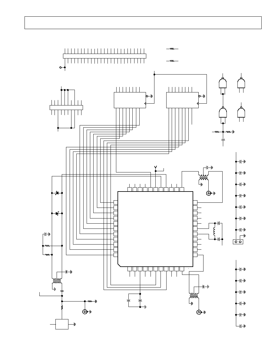
The schematic of the evaluation board (Figure 25) represents a
typical implementation of the AD6600. A multilayer board is
recommended to achieve best results. It is highly recommended
that high quality, ceramic chip capacitors be used to decouple
each supply pin to ground directly at the device. The pinout of
the AD6600 facilitates ease of use in the implementation of high
frequency, high resolution design practices. All of the digital
outputs are segregated to two sides of the chip, with the inputs
on the opposite side for isolation purposes.
Care should be taken when routing the digital output traces. To
prevent coupling through the digital outputs into the analog
portion of the AD6600, minimal capacitive loading should be
placed on these outputs. It is recommended that a fanout of
only one be used for all AD6600 digital outputs.
The layout of the analog inputs and the external resonant filter
are critical. No digital traces must be routed near, under, or
above these portions of the circuit. The transformers used for
coupling into the analog inputs must be located as close as
possible to the analog inputs of the AD6600. The external reso-
nant filter components must be physically close to the filter-
input pins, yet separated from the analog inputs.

REV. 0
AD6600
20
The layout of the Encode circuit is equally critical. Any noise
received on this circuitry will result in corruption in the digitiza-
tion process and lower overall performance. The Encode clock
must be isolated from the digital outputs and the analog inputs.
Evaluation Board
The evaluation board for the AD6600 is straightforward, con-
taining all required circuitry for evaluating the device. The only
external connections required are power supplies, clock and the
analog inputs. The evaluation board includes the option for an
on-board, clock oscillator for encode.
Power to the analog supply pins of the AD6600 is connected via
the power terminal block (TB1). Power for the digital interface
is supplied via Pin 1 of J201, or the VDD e-hole located adja-
cent to J201. The VDD supply can vary between 3.3 V to 5.0 V
and sets the level for the output digital data (J201). The J201
connector mates directly with the AD6620 (Receive Signal
Processor) evaluation board, Part # AD6620S/PCB, allowing
complete evaluation of system performance.
The two analog inputs are connected via SMA connectors
AIN and BIN, which are transformer-coupled to the AD6600
inputs. The transformers have a turns-ratio of 1:4 to match
the input resistance of the AD6600 (200
) to 50 at the
SMA connectors.
The Encode signal may be generated using an on-board crystal
oscillator, U100. If an on-board crystal is used, R104 must be
removed from the board to prevent loading of the oscillator's
output. The on-board oscillator may be replaced by an external
encode source via the SMA connector labeled ENCODE. If an
external source is used, it must be a high quality and very low
phase noise source. The high IF range of the AD6600 (70 MHz
250 MHz) demands that the Encode clock be sufficiently pure
to maintain performance.
The AD6600 output data is latched using 74LCX574 (U201,
U202) latches. The clock for these latches is determined by
jumper selection on header J1. The clock can be a delayed ver-
sion of the encode clock (CLKA, CLKB), or the CLK2
× gener-
ated by the AD6600. A clock is also distributed with the output
data (J201) that is labeled CLKX (Pin 11, J201). The CLK
× is
selected with jumpers on header J1 and can be CLKA, CLKB,
or CLK2
×.
The resonant LC filter components (SEL2, C2 and C3) are
omitted. The user must install proper values based on the IF
chosen. See Understanding the External Analog Filter section of
the data sheet for guidelines on selecting these components.
Table VI. AD6600ST/PCB Bill of Material
Item
Quantity
Reference
Description
1
3
AIN, BIN, ENCODE
SMA Connector
2
14
C1, C102108, C114, C117118,
Ceramic Chip Capacitor 1206, 0.1
µF
C120121, C299
3
2
C100101
Tantalum Chip Capacitor, 10
µF
4
1
C111
Ceramic Chip Capacitor 0805, 0.1
µF
5
4
C112C113, C115116
Ceramic Chip Capacitor 0508, 0.1
µF
6
2
CR12
1N2810 Schottky Diode
7
1
DUT
AD6600AST
8
1
J1
20-Pin Double Row Male Header
9
1
J201
50-Pin Double Row Male Header, Right Angle
10
2
R12
Omitted
11
2
R100R101
Surface Mount Resistor 1206, 10 k
12
1
R103
Surface Mount Resistor 1206, 100
13
1
R104
Surface Mount Resistor 1206, 50
14
2
R298R299
Surface Mount Resistor 1206, 2 k
15
3
T1T2, T4
Surface Mount Transformer Mini-Circuits T41T
16
1
TB1
PCTB2 Terminal Block
17
2
U201U202
74LCX574 Octal Latch
18
1
U204
74LVQ00 Two Input NAND Gate
REV. 0
AD6600
21
AD6600AST
29
30
31
32
33
27
28
25
26
23
24
DVCC
GND
AVCC
GND
AB_OUT
CLK2X
ENC
ENC
AVCC
GND
BIN
3
4
5
6
7
1
2
10
11
8
9
DVCC
GND
C1
AVCC
GND
RSSI2
RSSI1
RSSI0
B_SEL
A_SEL
AIN
4
0
39
38
41
42
43
44
36
3
5
3
4
37
D10
D9
D8
D7
D6
D5
D4
D3
D2
D1
D0
(MSB)
(LSB)
12
13
1
4
1
5
1
6
1
7
1
8
19
20
2
1
2
2
GND
AVCC
GND
FLT
GND
AVCC
AVCC
FLT
AVCC
AIN
BIN
VDD
GND
VCC
GND
B
A
C111
0.1
F
C112
0.01
F
SMA
AIN
4
6
3
1
2
C115
0.01
F
SEL2
C3
SEL
C2
SEL
VCC
GND
VCC
VCC
VCC
GND
VCC
GND
SMA
BIN
4
6
3
1
2
C116
0.01
F
VDD
GND
VCC
GND
VCC
GND
SMA
ENCODE
4
6
3
1
2
C113
0.01
F
C1
0.1
F
R1
R2
CR1
1N2810
CR2
1N2810
C114
0.1
F
CLKREF
R104
50
R103
100
OUT
V
CC
VEE
VCC
U100
14
7
8
K1115
2
CLK
CLK_2
8D
8Q
7D
7Q
6D
6Q
5D
5Q
4D
4Q
3D
3Q
2D
2Q
1D
1Q
CK
OE
12
13
14
15
16
17
18
19
A/B
BIT0
BIT1
BIT2
BIT3
BIT4
BIT5
BIT6
11
1
CLK
U201
74LCX574
8D
8Q
7D
7Q
6D
6Q
5D
5Q
4D
4Q
3D
3Q
2D
2Q
1D
1Q
CK
OE
12
13
14
15
16
17
18
19
BIT7
BIT8
BIT9
BIT10
RSSIB2
RSSIB1
RSSIB0
11
1
U202
74LCX574
9
8
7
6
5
4
3
2
9
8
7
6
5
4
3
2
D10
D9
D8
D7
D6
D5
D4
D3
D2
D1
D0
RSSI0
RSSI1
RSSI2
A/B
A/B
D0
D1
D2
D3
D4
D5
D6
D7
D8
D9
D10
RSSI2
RSSI1
RSSI0
1
2
3
4
5
6
7
8
9
10
20
19
18
17
16
15
14
13
12
11
H20DM
J1
A
B
CLK
CLKA
CLK_2X
CLKB
GND
GND
CLKA
CLKB
CLKX
50
1
24
9
34
8
44
7
54
6
64
5
74
4
84
3
94
2
10
41
11
40
12
39
13
38
14
37
15
36
16
35
17
34
18
33
19
32
20
31
21
30
22
29
23
28
24
27
25
26
H50DM
J201
V
DD
BIT10
BIT9
BIT8
BIT7
BIT6
BIT5
BIT4
BIT3
CLK
CLKX
BIT2
BIT1
BIT0
GND
GND
GND
GND
GND
GND
GND
RSSIB2
RSSIB1
RSSIB0
GND
GND
GND
GND
GND
GND
GND
GND
GND
GND
GND
GND
GND
GND
GND
GND
GND
GND
GND
GND
GND
GND
GND
GND
A/B
GND
R100
10k
A
VCC
R101
10k
B
VCC
1
2
3
R298
2
R299
2k
V
DD
C299
0.1
F
CLKREF
U204
74LVQ00
9
10
8
U204
74LVQ00
GND
GND
12
13
11
U204
74LVQ00
GND
GND
4
5
6
U204
74LVQ00
CLKA
1
2
TB1
PCTB2
+
C100
C102
C104
C106
C108
C120
C121
VCC
+
C101
C103
C105
C107
C117
C118
VDD
1:4
T4
TI
4T
TI
4T
1:4
T2
T1
4T
1:4
GND
REMOVE 21 AND 30
T1
Figure 25. AD6600ST/PCB Schematic Diagram
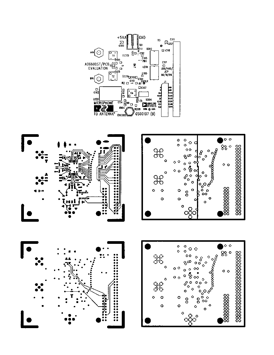
REV. 0
AD6600
22
Figure 27. AD6600ST/PCB Top Side Copper
Figure 28. AD6600ST/PCB Bottom Side Copper
Figure 29. AD6600ST/PCB Power Supply Layer (Negative)
Figure 30. AD6600ST/PCB Ground Layer (Negative)
Figure 26. AD6600ST/PCB Top Side Silk Screen
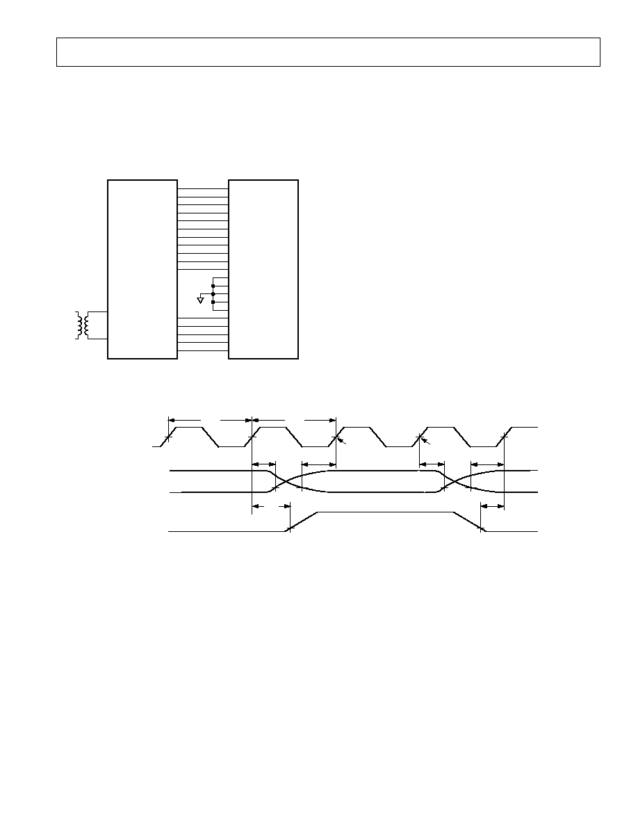
REV. 0
AD6600
23
Connecting the AD6600 with the AD6620
The AD6600 interfaces directly to the AD6620 Digital Receive
Signal Processor as shown in Figure 31. No additional external
components are required. Note that the layout requirements dis-
cussed previously do apply and deviations can result in degraded
performance. The digital outputs of the AD6600 must connect
directly to the AD6620 inputs with no additional fanout. Addi-
tional loading on the outputs will compromise timing performance.
AD6600
AD6620
(MSB) D10
D3
D2
D1
(LSB) D0
D9
D8
D7
D6
D5
D4
IN15
IN14
IN13
IN12
IN11
IN10
IN9
IN8
IN7
IN6
IN5
IN4
IN3
IN2
IN1
IN0
EXP2
EXP1
EXP0
A/B
CLK
RSSI2
RSSI1
RSSI0
AB_OUT
CLK2
ENC
ENC
Figure 31. AD6600/AD6620 Connections
Figure 32 shows the timing details between the AD6600 and the
AD6620. On Clock 1, D[10:0], RSSI[2:0], and AB_OUT are
captured by the AD6620. Since AB_OUT has changed state from
the previous clock, the D[10:0] and RSSI[2:0] are processed by
the AD6620. This clock allows adequate setup and hold time
for AB_OUT, D[10:0], and RSSI[2:0] to be captured by the
AD6620.
On Clock2, D[10:0], RSSI[2:0], and AB_OUT are captured
by the AD6620. Since AB_OUT has not changed from the
previous clock, the D[10:0] and RSSI[2:0] are ignored by the
AD6620. This clock is concerned only with the AB_OUT setup-
and-hold time.
CLK2
D [10:0]
RSSI [2:0]
AB_OUT
38.5
38.5
3.0
16.5
7.0
3.0
16.5
12.5
CLOCK1
CLOCK2
Figure 32. AD6600 to AD6620 Timing at 13 MSPS
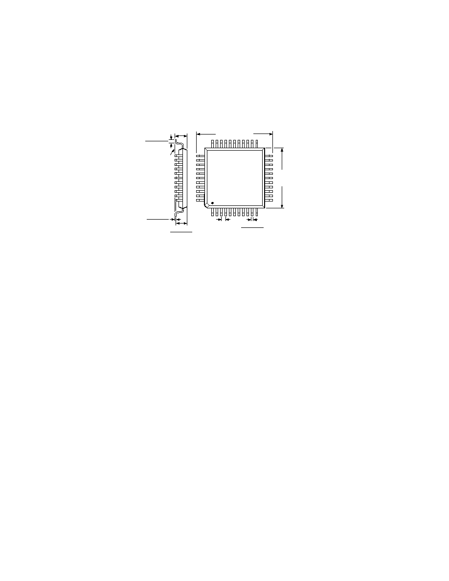
REV. 0
AD6600
24
C009662.57/00 (rev. 0)
PRINTED IN U.S.A.
44-Terminal LQFP (Low-Profile Quad Plastic Flatpack)
(ST-44)
TOP VIEW
(PINS DOWN)
1
33
34
44
11
12
23
22
0.018 (0.45)
0.012 (0.30)
0.031 (0.80)
BSC
0.394
(10.0)
SQ
0.472 (12.00) SQ
0.057 (1.45)
0.053 (1.35)
0.006 (0.15)
0.002 (0.05)
SEATING
PLANE
0.063 (1.60)
MAX
0.030 (0.75)
0.018 (0.45)
OUTLINE DIMENSIONS
Dimensions shown in inches and (mm).