Äîêóìåíòàöèÿ è îïèñàíèÿ www.docs.chipfind.ru
REV. 0
Information furnished by Analog Devices is believed to be accurate and
reliable. However, no responsibility is assumed by Analog Devices for its
use, nor for any infringements of patents or other rights of third parties
which may result from its use. No license is granted by implication or
otherwise under any patent or patent rights of Analog Devices.
a
AD6140
One Technology Way, P.O. Box 9106, Norwood, MA 02062-9106, U.S.A.
Tel: 781/329-4700
World Wide Web Site: http://www.analog.com
Fax: 781/326-8703
© Analog Devices, Inc., 1998
Bandpass
IF Subsystem
FUNCTIONAL BLOCK DIAGRAM
MIXER POST
AMPLIFIER
MIXER
MODULATOR
AGC
DETECTOR
CIRCUIT
ECL-TO-CMOS
LEVEL-SHIFTER
LNA BIAS
AMPLIFIER
PREAMPLIFIER
IF_INPUT
LNA_SENSE
LNA_FORCE
_DATA_OUT
_CLOCK_OUT
BUFFER_VDD
CLK_IN+
CLK_IN
BUFFER_GND
AVDD AGND DGND DVDD POWER_DOWN
AGC_CAPACITOR
0.1 F
BIAS_RESISTOR
39k
R
INT
BIAS SYSTEM
AGC_TC_SELECT
VOLTAGE_REFERENCE_IN
AD6140
LO_IN+
LO_IN
FEATURES
IF Subsystem
Bandpass
Modulator
Variable-Gain Preamplifier with 13 dB of AGC Range
Mixer
AGC Detector
Op Amp for LNA Biasing
ECL-to-CMOS Level Translator
Ultralow Power Design
2.7 V Operating Voltage
4.8 mA Current Consumption
Power-Down Control
Small 20-Lead SSOP Package
APPLICATIONS
FLEXTM, ReFLEXTM Receivers
Multimode Receivers
GENERAL DESCRIPTION
The AD6140 is a bandpass
ADC IF IC for receivers requiring
a high dynamic range and multiple filter bandwidths. With an
external decimation filter, it creates a multibit analog-to-digital
converter. The AD6140 consists of a variable gain, low noise
preamplifier, mixer, AGC detector, bandpass
modulator, an
ECL-to-CMOS level translator for the system clock, and an
auxiliary amplifier for use in biasing a discrete LNA. It is de-
signed to operate with Motorola's ReFLEX chipset solution.
Contact Motorola directly for more information about the
ReFLEX chipset solution. With data and clock outputs at CMOS
logic levels, it interfaces to an external decimation filter. It comes in
a 20-lead plastic SSOP and operates over the 40
°
C to +85
°
C
industrial temperature range at 2.7 V.
FLEX and ReFLEX are trademarks of Motorola, Inc.

REV. 0
2
AD6140SPECIFICATIONS
(T
A
= +25 C, V
CC
= 2.7 V, VOLTAGE_REFERENCE_IN = 1 V, unless otherwise noted)
Specification
Conditions
Min
Typ
Max
Units
OVERALL
VOLTAGE_REFERENCE_IN = 1 V
±
5% dc,
IF = 49.6 MHz
LO = 49.792 MHz or 49.408 MHz, 200 mV p-p
Differential Input
Clock = 6.144 MHz, 800 mV p-p Differential ECL
Input, Clock Asymmetry = 50
±
2.5%
Input Third Order Intercept Point
At Max Gain
27
19
dBm
Noise Figure
At Max Gain, External Termination
10.5
dB
Input Resistance
At IF_INPUT (Pin 19)
2.5
k
Input Capacitance
At IF_INPUT (Pin 19)
12
pF
Dynamic Range
6.25 kHz Bandwidth Centered at 192 kHz
76
83
dB
Maximum Gain
29.5
dB
Minimum Gain
16
dB
AGC DETECTOR
AGC Threshold
24
dBm
Capacitor Charging Current
AGC_TC_SELECT Input = Logic LOW (FAST AGC)
2.8
µ
A
AGC_TC_SELECT Input = Logic HIGH (SLOW AGC)
50
nA
ECL-TO-CMOS LEVEL
VDD (to VDD 0.8 V) Differential Levels
TRANSLATOR
Clock Output Drive
5 pF Load
2.6
V p-p
Clock Asymmetry
5 pF Load
±
2.5
%
LNA BIAS AMPLIFIER VOLTAGE
LNA_FORCE
2.9 V
LNA_SENSE, Minimum Gain
1.7
V
LNA_SENSE Input Voltage Range
VDD
VDD 0.3
V
POWER-DOWN INTERFACE
Logic Threshold
0.7
V
Turn-On Response Time
To Valid Data Output
100
µ
s
Turn-Off Response Time
To Typical Power-Down Supply Current
100
µ
s
POWER SUPPLY
Supply Voltage
2.5
2.9
V
Supply Current
Power-Down Input: Logic LOW = ON, IF_Input = 0 V
4.8
5.75
mA
Power-Down Current
Power-Down Input: Logic HIGH = OFF
3
µ
A
Operating Temperature Range
40
+85
°
C
Specifications subject to change without notice.
REV. 0
AD6140
3
CAUTION
ESD (electrostatic discharge) sensitive device. Electrostatic charges as high as 4000 V readily
accumulate on the human body and test equipment and can discharge without detection.
Although the AD6140 features proprietary ESD protection circuitry, permanent damage may
occur on devices subjected to high energy electrostatic discharges. Therefore, proper ESD
precautions are recommended to avoid performance degradation or loss of functionality.
WARNING!
ESD SENSITIVE DEVICE
ABSOLUTE MAXIMUM RATINGS
1
Supply Voltage to Ground . . . . . . . . . . . . . . . . . . . . . . +5.5 V
Internal Power Dissipation
2
. . . . . . . . . . . . . . . . . . . . 50 mW
Operating Temperature Range . . . . . . . . . . . 40
°
C to +85
°
C
Storage Temperature Range . . . . . . . . . . . . 65
°
C to +150
°
C
Lead Temperature, Soldering (60 sec) . . . . . . . . . . . . +300
°
C
NOTES
1
Stresses above those listed under Absolute Maximum Ratings may cause perma-
nent damage to the device. This is a stress rating only; functional operation of the
device at these or any other conditions above those indicated in the operational
section of this specification is not implied. Exposure to absolute maximum rating
conditions for extended rating conditions for extended periods may affect device
reliability.
2
Thermal Characteristics:
20-Lead SSOP:
JA
= 126
°
C/W.
PIN CONFIGURATION
TOP VIEW
(Not to Scale)
20
19
18
17
16
15
14
13
12
11
1
2
3
4
5
6
7
8
9
10
AD6140
AGC TC SELECT
POWER DOWN
BUFFER VDD
LNA SENSE
CLK IN+
CLK IN
CLOCK OUT
DATA OUT
BUFFER GND
DVDD
DGND
AGC CAPACITOR
IF INPUT
AGND
VOLTAGE REFERENCE IN
LO IN+
LO IN
BIAS RESISTOR
LNA FORCE
AVDD
ORDERING GUIDE
Temperature
Package
Package
Model
Range
Description
Option
AD6140ARS
40
°
C to +85
°
C
Shrink Small Outline Package
RS-20
AD6140ARSRL
40
°
C to +85
°
C
20-Lead Plastic SSOP on Tape-and-Reel

REV. 0
AD6140
4
PIN FUNCTION DESCRIPTION
Pin
Pin
No
Name
Function
Applicable Signal Levels
1
LNA_FORCE
Output For Biasing Discrete LNA
Output Ranges from 0 V (LNA OFF) to 2.7 V
2
LNA_SENSE
Input For Biasing Discrete LNA
VDD to VDD 0.3 V Input
3
CLK_IN+
Positive 6.144 MHz ADC Clock Input
800 mV p-p Differential Input
VDD to VDD 0.8 V Levels
Direct Coupled into 1500
Impedance
4
CLK_IN
Negative 6.144 MHz ADC Clock Input
800 mV p-p Differential Input
VDD to VDD 0.8 V Levels
Direct Coupled into 1500
Impedance
5
BUFFER_GND
ECL-to-CMOS Level Translator Ground
Pin Connected to Ground
6
_DATA_OUT
ADC Serial Data Output
CMOS Logic Levels
7
_CLOCK_OUT
6.144 MHz ADC Clock Output
CMOS Logic Levels
8
BUFFER_VDD
ECL-to-CMOS Level Translator VDD
Digital Supply Input
9
POWER_DOWN
Turns IC Off and On
CMOS Logic Levels; 0 V = ON, VPOS = OFF
10
AGC_TC_SELECT
AGC Time Constant Select; Changes
CMOS Logic Levels; 0 V = Fast Mode,
AGC Capacitor Charging Current by 56:1,
VPOS = Slow Mode
where FAST AGC Current is 56
×
SLOW
AGC Current
11
DVDD
Digital Power Supply Input
Pin Connected to Digital Supply
12
DGND
Digital Ground
Pin Connected to Ground
13
AGC_CAPACITOR
Charge/Discharge Current into AGC
AGC Integration Capacitor
Integrator Capacitor
Connected to Ground
14
LO_IN+
Positive LO Input
200 mV p-p Differential Input; Internally
AC-Coupled into 1500
Impedance
15
LO_IN
Negative LO Input
200 mV p-p Differential Input, Internally
AC-Coupled into 1500
Impedance
16
BIAS_RESISTOR
Resistor to Ground Sets Overall Bias
39 k
Resistor Connected to Ground
Current and Power Consumption
17
VOLTAGE_REFERENCE_IN
ADC Voltage Reference Input
Regulated and Filtered 1.0 V
±
5% Input
18
AGND
Analog Ground
Pin Connected to Ground
19
IF_INPUT
IF Input
Typically 16.4
µ
V p-p to 65.2 mV p-p
20
AVDD
Analog Power Supply Input
Pin Connected to Analog Supply
REV. 0
AD6140
5
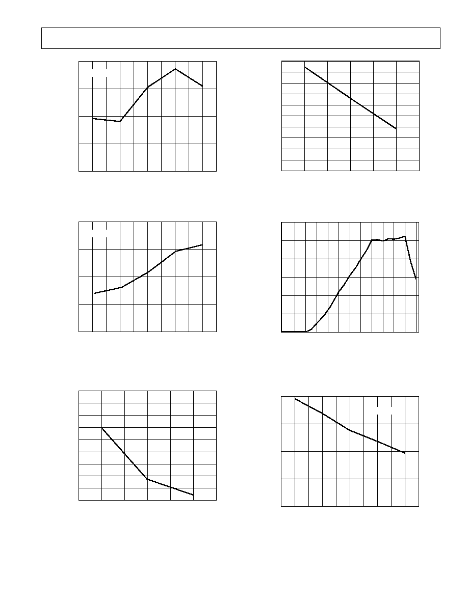
TEMPERATURE C
12
10
8
40
NOISE FIGURE dB
11
9
20
25
60
85
V
CC
= +2.7V
Figure 1. Noise Figure vs. Temperature
SUPPLY VOLTAGE Volts
12.0
11.0
10.0
2.5
NOISE FIGURE dB
11.5
10.5
2.6
2.7
2.8
2.9
T = +25 C
Figure 2. Noise Figure vs. Power Supply
SUPPLY VOLTAGE Volts
19.20
2.5
INPUT IP3 dBm
2.6
2.7
2.8
2.9
19.25
19.30
19.35
19.40
19.45
19.50
19.55
19.60
19.65
Figure 3. Input IP3 vs. Power Supply
Typical Performance Characteristics
TEMPERATURE C
21.0
40
INPUT IP3 dBm
25
85
20.5
20.0
19.5
19.0
18.5
18.0
17.5
17.0
16.5
16.0
Figure 4. Input IP3 vs. Temperature
\
IF INPUT LEVEL dBm
60
20
0
120
SNR dB
30
10
112
108
100
9
0
8
0
7
0
6
0
5
0
4
0
3
0
2
3
1
9
40
50
Figure 5. Signal to Noise Ratio vs. IF Input Level at
T
A
= +25
°
C
TEMPERATURE C
4.9
4.7
40
CURRENT mA
4.8
20
25
60
85
V
CC
= +2.7V
Figure 6. Supply Current vs. Temperature
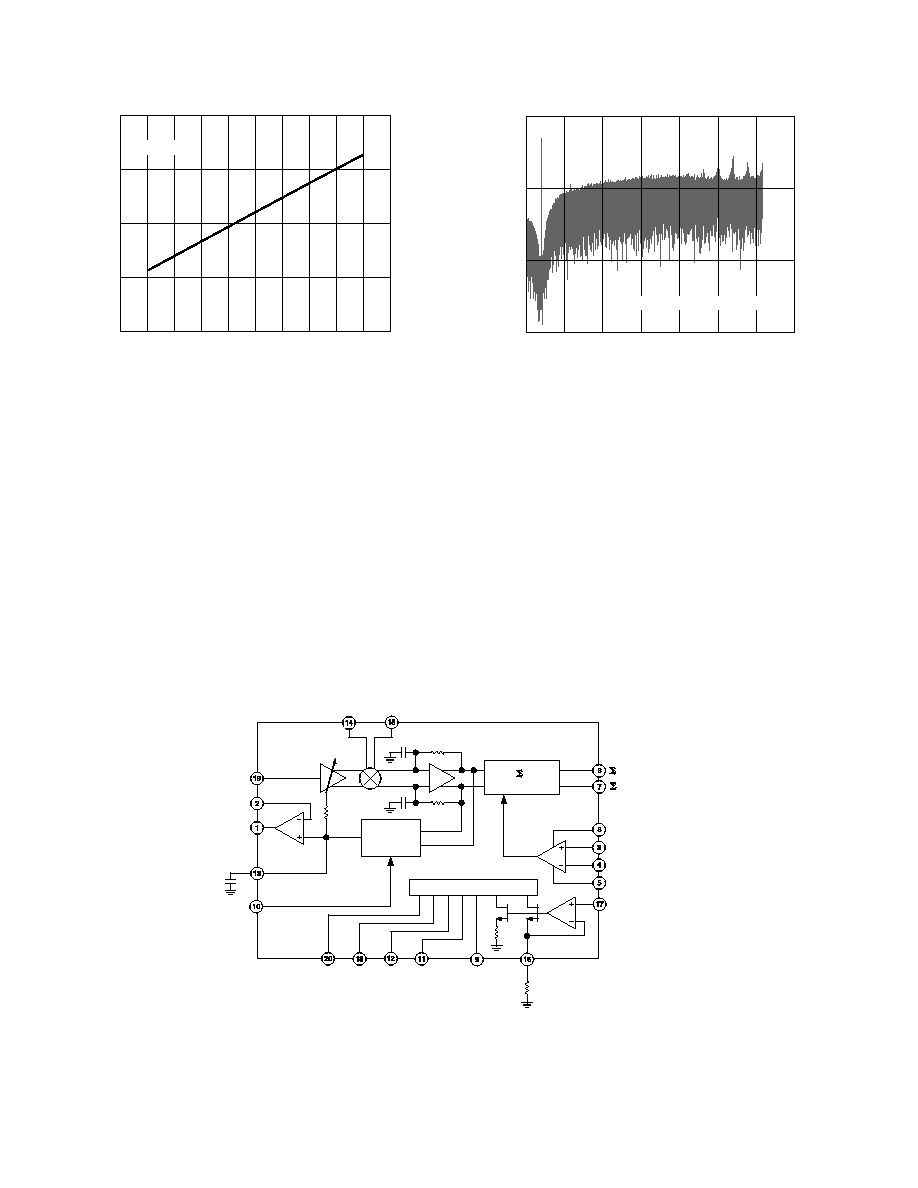
REV. 0
AD6140
6
POWER SUPPLY VOLTAGE Volts
5.2
4.8
4.4
2.5
CURRENT mA
5.0
4.6
2.6
2.7
2.8
2.9
T
A
= +25 C
Figure 7. Supply Current vs. Power Supply Voltage
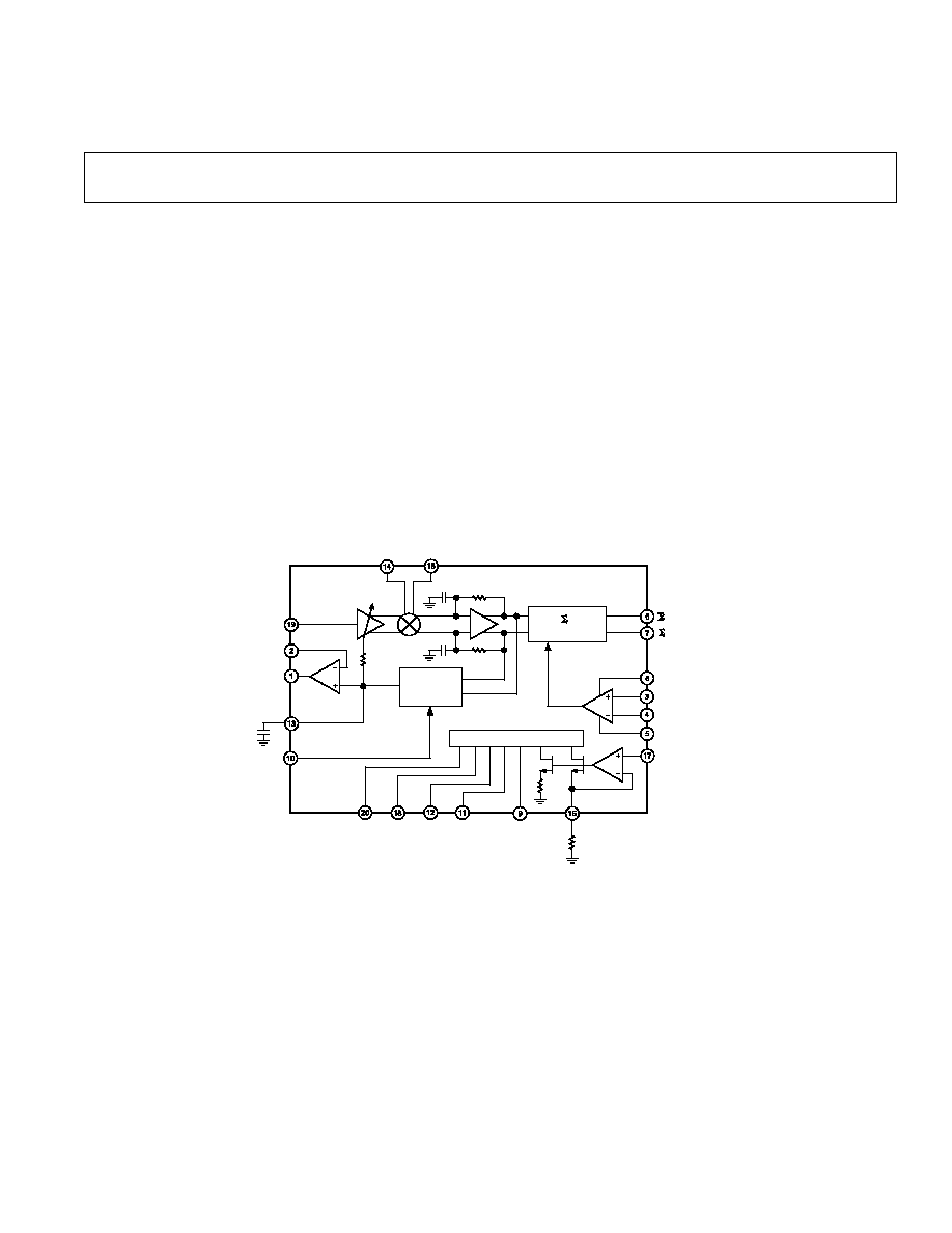
MIXER POST
AMPLIFIER
MIXER
MODULATOR
AGC
DETECTOR
CIRCUIT
ECL-TO-CMOS
LEVEL-SHIFTER
LNA BIAS
AMPLIFIER
PREAMPLIFIER
IF_INPUT
LNA_SENSE
LNA_FORCE
_DATA_OUT
_CLOCK_OUT
BUFFER_VDD
CLK_IN+
CLK_IN
BUFFER_GND
AVDD AGND DGND DVDD POWER_DOWN
AGC_CAPACITOR
0.1 F
BIAS_RESISTOR
39k
R
INT
BIAS SYSTEM
AGC_TC_SELECT
VOLTAGE_REFERENCE_IN
AD6140
LO_IN+
LO_IN
Figure 8. Functional Block Diagram
MODULATION
A
modulator
uses feedback around a low noise quantizer
(1 bit in this case) in order to "shape" the spectrum of quantiza-
tion noise. Using this technique, we can shape noise away from
an arbitrary passband, within which we can place a modulated
signal. A
modulator reproduces the input, but adds quanti-
zation noise, which can be digitally removed with a filter, known
as a decimation filter. Applying this technique to bandpass
signals results in an analog-to-digital converter suitable for
converting the IF signals in a digital radio.
The output of the AD6140's
modulator is shown in Figure
9. As can be seen, the noise is shaped away from a narrow band-
width, within which we place a signal (a sine wave in this case)
resulting in a narrowband, high dynamic range digital represen-
tation of the analog input.
FREQUENCY kHz
0
100
150
0
OUTPUT LEVEL dB
50
500
1000
1500
2000
2500
3000
3500
RESPONSE FROM 0kHz TO (f
S
/2)kHz
Figure 9. Output Spectrum of AD6140
PRODUCT OVERVIEW
The AD6140 is a bandpass
analog-to-digital converter IF
IC for dual conversion receivers requiring a high dynamic range
and multiple filter bandwidths. It consists of a variable gain, low
noise preamplifier, mixer, automatic gain control (AGC) detec-
tor, bandpass
modulator, an ECL to CMOS level translator
and an auxiliary amplifier for use in biasing a discrete LNA.
The low noise preamplifier accepts a first IF input at 49.6 MHz
from 16.4
µ
V p-p to 63.2 mV p-p. It provides a variable gain
from 12 dB to 25 dB.
The mixer accepts an LO frequency of 49.792 MHz or
49.408 MHz, resulting in an IF frequency of 192 kHz. The LO
level should be 200 mV p-p differential. It is ac-coupled to the
AD6140. The mixer operates in the linear region, hence the
gain of the mixer is a function of the LO level. As a result, spe-
cial care must be taken to ensure that the LO level is 200 mV p-p,

REV. 0
AD6140
7
otherwise, the expected gain will not be obtained from the
AD6140. In addition to the mixer, there is a mixer post-
amplifier within the AD6140. The total gain from the mixer
and mixer post-amplifier is 5 dB.
The
modulator uses a 6.144 MHz clock, which is a differen-
tial ECL input. There is an ECL-to-CMOS converter on the
AD6140, which converts this differential ECL input into a
single-ended CMOS signal. This 6.144 MHz single-ended CMOS
clock is provided at Pin 7 (
_CLOCK_OUT). The output
data of the AD6140 is a 6.144 MHz single bitstream at Pin 6
(
_DATA_OUT). The signal gain through the
modulator
is 0.77 dB.
Within the
modulator, the data output digital bitstream is
fed through a 1-bit D/A converter and is fed back to numerous
internal points. The level of this feedback signal, known as the
full-scale level, defines the
modulator input signal level,
which would result in the output digital bitstream containing the
maximum number of ones possible. This condition, known as
maximum ones density, represents the maximum in-band out-
put signal power of the
modulator. The full-scale level is set
to 2 V p-p or 4.77 dBm (relative to 1500
). However, if a
signal into the modulator is 4.77 dBm, the modulator will
enter an unstable state. Consequently, the maximum input to
the modulator is constrained to 5 dB less than the signal, which
would produce maximum ones density. This level, defined as
the clip level, is 9.77 dBm (relative to 1500
).
The maximum signal into the modulator does not correspond to
maximum ones density. The entire dynamic range of the result-
ing analog to digital converter (
modulator plus decimation
filter) is not realized. In order to relate the maximum signal into
the modulator to the maximum signal out of the modulator, a
gain of 5 dB should be applied in the decimation filter.
As can be seen in Figure 5, the output signal to noise ratio will
increase until a point at which it rapidly degrades. This point
represents the input signal level where the
modulator has
become unstable. As a result, the maximum input signal level is
constrained by the point at which it is so high that instability
occurs in the modulator. Dynamic range is defined as the differ-
ence between the integrated noise floor (within a particular
bandwidth) and the power in the output signal just before the
modulator has become unstable. For a typical 6.25 kHz
bandwidth centered around 192 kHz, the AD6140 has 83 dB of
dynamic range.
In order to increase the range of useful input signals of the
AD6140, an AGC detector is employed which senses the input
signal level to the
modulator and adjusts the gain in the pream-
plifier. The AGC circuitry provides 13 dB of automatic gain
control range. The AGC operates when the internal AGC voltage
is between 700 mV (minimum gain) and 1.55 V (maximum gain).
This voltage can be measured on the AGC_CAPACITOR pin
(Pin 13).
The AD6140 can be configured with the chip powered up or
down. In order to power the chip down, set pin POWER_DOWN
(Pin 9) high. In order to power it up, set pin POWER_DOWN
(Pin 9) low.
Finally, an auxiliary amplifier used for biasing an external dis-
crete LNA is provided with the AD6140.
FREQUENCY PLAN
The AD6140 and its
modulator are designed for a specific
frequency plan: a 6.144 MHz master clock, a 49.6 MHz first
IF input, and a 192 kHz center frequency in the bandpass
modulator. The local oscillator may use high-side or low-side
injection. The specifications for the AD6140 are only valid for
this frequency plan. Any deviation from this frequency plan may
result in degradation of the specified performance. Furthermore,
there are only specific frequency plans which will result in ac-
ceptable performance for most applications. To avoid problems,
do not change the frequency plan.
USING THE AD6140
In this section, we will examine a few areas of special impor-
tance and include a few general applications tips. As is true of
any device operating in the IF frequency range, special care
must be taken in PC board layout. The location of the particular
grounding points must be considered, with the objective of
minimizing any unwanted signal coupling. Specifically, care
should be taken in the layout of the IF and LO signal paths as
well as the data and clock digital bit-streams. Layout of these
portions of the PC board require special attention in order to
ensure that the high frequency portions of these signals do not
couple into other signals in the system. In order to maintain
balance in differential signal levels, be sure to keep short and
equal length transmission lines.
The power supplies should be decoupled to ensure a clean dc
signal. Special care should be taken with respect to ensuring that
the BUFFER_VDD is especially clean and at the appropriate
levels since the output in-band noise floor is particularly sensi-
tive to this supply.
The IF input signal should be impedance matched and ac
coupled. The impedance looking into the IF input pin is typi-
cally a 2.5 k
resistance in parallel with a 12 pF capacitance.
The 1 V reference signal should be regulated and filtered.
The value of the BIAS_RESISTOR (Pin 16) is 39 k
. The bias
resistor sets the current consumption of the AD6140. Because
the AD6140 was characterized with a 39 k
bias resistor, this is
the only value for which the AD6140 specifications are guaran-
teed. Maximum current consumption is measured when the
AD6140 is operating at maximum gain.
The AGC integration capacitor should be large enough to by-
pass any externally-generated noise on the internal AGC line to
ground in addition to providing a path for the charging and
discharging of the AGC current. In the Motorola ReFLEX
chipset solution, this capacitor is 0.1
µ
F. The AGC time con-
stant is switch-selectable with the AGC_TC_SELECT pin (Pin
10). The AGC time constant has a typical current ratio of 56:1
when in the fast mode relative to slow mode. The nominal
AGC current in the fast (high current) position is 2.8
µ
A and
in the slow (low current) position is 50 nA. The AGC time
constant may be calculated from Equation 1.
T
CV
I
=
(1)
where T is the AGC time constant in seconds, C is the value of
the AGC capacitor in Farads, V is the full-scale change in the
AGC voltage, and I is the charging current in amperes.
REV. 0
AD6140
8
C3436310/98
PRINTED IN U.S.A.
LEVEL DIAGRAM
Figure 10 shows a simplified block diagram of the AD6140 with
the expected signal levels for the minimum gain configuration.
MIXER POST
AMPLIFIER
MIXER
LOCAL
OSCILLATOR INPUT
49.792MHz
16.3 dBm REFERRED TO 50
MODULATOR
AGC
DETECTOR
CIRCUIT
PREAMPLIFIER
IF INPUT
f = 49.6MHz
60mV p-p
DATA OUT
378mV p-p
AT 192kHz
Figure 10. Level Diagram
OUTLINE DIMENSIONS
Dimensions shown in inches and (mm).
20-Lead SSOP
(RS-20)
20
11
10
1
0.295 (7.50)
0.271 (6.90)
0.311 (7.9)
0.301 (7.64)
0.212 (5.38)
0.205 (5.21)
PIN 1
SEATING
PLANE
0.008 (0.203)
0.002 (0.050)
0.07 (1.78)
0.066 (1.67)
0.0256
(0.65)
BSC
0.078 (1.98)
0.068 (1.73)
0.009 (0.229)
0.005 (0.127)
0.037 (0.94)
0.022 (0.559)
8
0
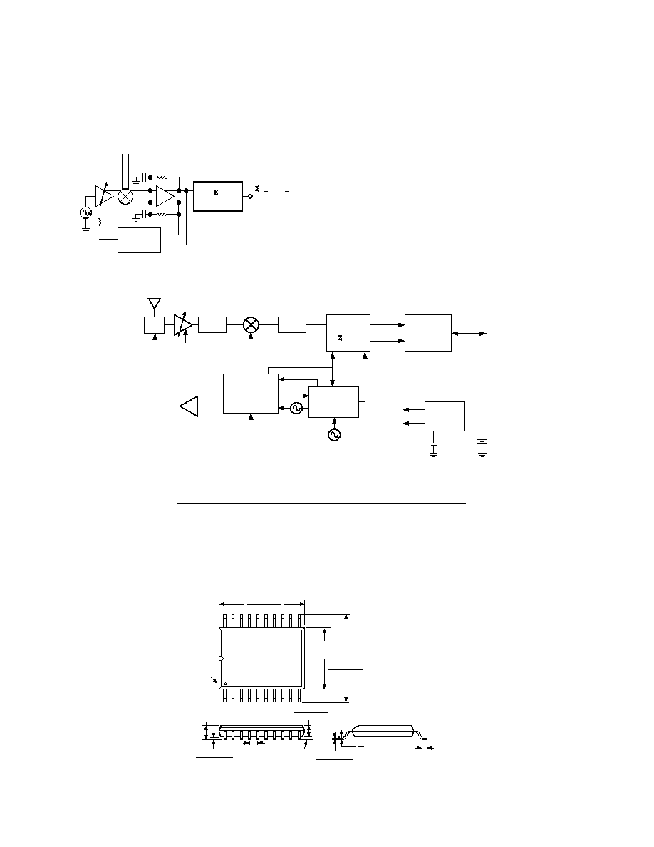
Motorola ReFLEX Transceiver
Figure 11 shows a block diagram of the Motorola ReFLEX
chipset solution including the AD6140. As can be seen, the
AD6140 accepts an IF input from a crystal filter at 49.6 MHz.
The frequency synthesizer provides the 6.144 MHz clock, while
the LO is also generated from the frequency synthesizer but is
fed to the AD6140 via the I/Q modulator. The IF data output
and the clock output both feed into the IF data processor. The
LNA bias amplifier provides the AGC voltage for the first LNA
in the receive path. The dc power is supplied from the power
management chip.
LNA
MAX847
PWR MGT
2.8V DV
DD
2.7V AV
DD
PRIMARY
BATTERY
TRANSMIT
POWER
SOURCE
Tx/Rx
SW
2.4V HBT
PA
SAW
FILTER
929-941MHz SC-4344-A
XTAL
FILTER
49.6MHz
AGC
1 WATT
986-902MHz
MC145181
FREQUENCY
SYNTHESIZER
TRF9506
I/Q
MODULATOR
76.8MHz
REF CLK
IF DATA
CLOCK
AD6140
A/D
IF DATA
PROCESSOR
SPI TO
REFLEX
CODEC
6.144MHz
SAMPLING
CLK
Tx DATA
Figure 11. ReFLEX Transceiver Block Diagram