Äîêóìåíòàöèÿ è îïèñàíèÿ www.docs.chipfind.ru
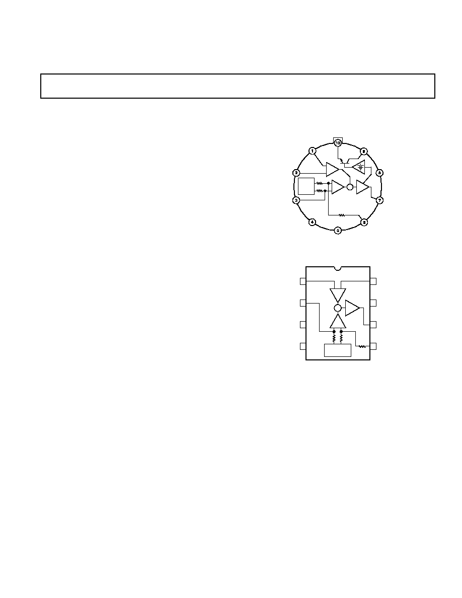
FUNCTIONAL BLOCK DIAGRAM
REV. B
Information furnished by Analog Devices is believed to be accurate and
reliable. However, no responsibility is assumed by Analog Devices for its
use, nor for any infringements of patents or other rights of third parties
which may result from its use. No license is granted by implication or
otherwise under any patent or patent rights of Analog Devices.
a
Thermocouple Conditioner and
Setpoint Controller
AD596*/AD597*
FEATURES
Low Cost
Operates with Type J (AD596) or Type K (AD597)
Thermocouples
Built-In Ice Point Compensation
Temperature Proportional Operation 10 mV/ C
Temperature Setpoint Operation ON/OFF
Programmable Switching Hysteresis
High Impedance Differential Input
GENERAL DESCRIPTION
The AD596/AD597 is a monolithic temperature setpoint con-
troller that has been optimized for use at elevated temperatures
such as those found in oven control applications. The device
cold junction compensates and amplifies a type J or K thermo-
couple input to derive an internal signal proportional to tem-
perature. The internal signal is then compared with an externally
applied setpoint voltage to yield a low impedance switched output
voltage. Dead-Band or switching hysteresis can be programmed
using a single external resistor. Alternately, the AD596/AD597 can
be configured to provide a voltage output (10 mV/
°
C) directly from
a type J or K thermocouple signal. It can also be used as a stand-
alone voltage output temperature sensor.
The AD596/AD597 can be powered with a single supply from
+5 V to +30 V, or dual supplies up to a total span of 36 V.
Typical quiescent supply current is 160
µ
A, which minimizes
self-heating errors.
The AD596/AD597 H package option includes a thermocouple
failure alarm that indicates an open thermocouple lead when
operated in the temperature proportional measurement mode.
The alarm output has a flexible format which can be used to
drive relays, LEDs or TTL logic.
The device is packaged in a reliability qualified, cost effective
10-pin metal can or SOIC and is trimmed to operate over an
ambient temperature range from +25
°
C to +100
°
C. Operation
over an extended ambient temperature range is possible with
slightly reduced accuracy. The AD596 will amplify thermo-
couple signals covering the entire 200
°
C to +760
°
C tempera-
ture range recommended for type J thermocouples while the
AD597 can accommodate 200
°
C to +1250
°
C type K inputs.
The AD596/AD597 has a calibration accuracy of
±
4
°
C at an
ambient temperature of 60
°
C and an ambient temperature
stability specification of 0.05
°
C/
°
C from +25
°
C to +100
°
C. If
higher accuracy, or a lower ambient operating temperature is
required, either the AD594 (J thermocouple) or AD595 (K
thermocouple) should be considered.
*Protected by U.S. Patent No. 4,029,974.
PRODUCT HIGHLIGHTS
1. The AD596/AD597 provides cold junction compensation
and a high gain amplifier which can be used as a setpoint
comparator.
2. The input stage of the AD596/AD597 is a high quality in-
strumentation amplifier that allows the thermocouple to float
over most of the supply voltage range.
3. Linearization not required for thermocouple temperatures
close to 175
°
C (+100
°
C to +540
°
C for AD596).
4. Cold junction compensation is optimized for ambient tem-
peratures ranging from +25
°
C to +100
°
C.
5. In the stand-alone mode, the AD596/AD597 produces an
output voltage that indicates its own temperature.
One Technology Way, P.O. Box 9106, Norwood, MA 02062-9106, U.S.A.
Tel: 781/329-4700
World Wide Web Site: http://www.analog.com
Fax: 781/326-8703
© Analog Devices, Inc., 1998
TO-100
+
G
FB
V
OUT
+ALM
+IN
V
V+
A
+
ICE
POINT
COMP
+
AD596/
AD597
ALM
IN
HYS
GND
+
G
SOIC
+IN
IN
TOP VIEW
(Not to Scale)
AD597
G
+
+
G
+
A
+
ICE POINT
COMP
HYS
V+
GND
V
OUT
V
FB
1
2
3
4
5
6
7
8

AD596/AD597SPECIFICATIONS
(@ +60 C and V
S
= 10 V, Type J (AD596), Type K (AD597) Thermocouple,
unless otherwise noted)
REV. B
2
Model
AD596AH
AD597AH
AD597AR
Min
Typ
Max
Min
Typ
Max
Min
Typ
Max
Units
ABSOLUTE MAXIMUM RATINGS
+V
S
to V
S
36
36
36
Volts
Common-Mode Input Voltage
(V
S
0.15)
+V
S
(V
S
0.15)
+V
S
(V
S
0.15)
+V
S
Volts
Differential Input Voltage
V
S
+V
S
V
S
+V
S
V
S
+V
S
Volts
Alarm Voltages
+ALM
V
S
(V
S
+36)
V
S
(V
S
+36)
V
S
(V
S
+36)
Volts
ALM
V
S
+V
S
V
S
+V
S
V
S
+V
S
Volts
Operating Temperature Range
55
+125
55
+125
40
+125
°
C
Output Short Circuit to Common
Indefinite
Indefinite
Indefinite
TEMPERATURE MEASUREMENT
(Specified Temperature Range
+25
°
C to +100
°
C)
Calibration Error
1
4
+4
4
+4
4
+4
°
C
Stability vs. Temperature
2
±
0.02
±
0.05
±
0.02
±
0.05
±
0.02
±
0.05
°
C/
°
C
Gain Error
1.5
+1.5
1.5
+1.5
1.5
+1.5
%
Nominal Transfer Function
10
10
10
mV/
°
C
AMPLIFIER CHARACTERISTICS
Closed Loop Gain
3
180.6
245.5
245.5
V/V
Input Offset Voltage
°
C
×
53.21 + 235
°
C
×
41.27 37
°
C
×
41.27 37
µ
V
Input Bias Current
0.1
0.1
0.1
µ
A
Differential Input Range
10
+50
10
+50
10
+50
mV
Common-Mode Range
(V
S
0.15)
(+V
S
4)
(+V
S
0.15)
(+V
S
4)
(V
S
0.15)
(+V
S
4)
Volts
Common-Mode SensitivityRTO
10
10
10
mV/V
Power Supply SensitivityRTO
1
10
1
10
1
10
mV/V
Output Voltage Range
Dual Supplies
(V
S
+ 2.5)
(+V
S
2)
(V
S
+ 2.5)
(+V
S
2)
(V
S
+ 2.5)
(+V
S
2)
Volts
Single Supply
0
(+V
S
2)
0
(+V
S
2)
0
(+V
S
2)
Volts
Usable Output Current
4
±
5
±
5
±
5
mA
3 dB Bandwidth
15
15
15
kHz
ALARM CHARACTERISTICS
5
Alarm Function Not Pinned Out
V
CE(SAT)
at 2 mA
0.3
0.3
Volts
Leakage Current
1
1
µ
A
Operating Voltage at ALM
(+V
S
4)
(+V
S
4)
Volts
Short Circuit Current
20
20
mA
POWER REQUIREMENTS
Operating
(+V
S
to V
S
)
30
(+V
S
to V
S
)
30
(+V
S
to V
S
)
30
Volts
Quiescent Current
+V
S
160
300
160
300
160
300
µ
A
V
S
100
200
100
200
100
200
µ
A
NOTES
1
This is a measure of the deviation from ideal with a measuring thermocouple junction of 175
°
C and a chip temperature of 60
°
C. The ideal transfer function is given by:
AD596: V
OUT
= 180.57
×
(V
m
V
a
+ (ambient in
°
C)
×
53.21
µ
V/
°
C + 235
µ
V)
AD597: V
OUT
= 245.46
×
(V
m
V
a
+ (ambient in
°
C)
×
41.27
µ
V/
°
C 37
µ
V)
where V
m
, and V
a
represent the measuring and ambient temperatures and are taken from the appropriate J or K thermocouple table. The ideal transfer function minimizes the
error over the ambient temperature range of 25
°
C to 100
°
C with a thermocouple temperature of approximately 175
°
C.
2
Defined as the slope of the line connecting the AD596/AD597 CJC errors measured at 25
°
C and 100
°
C ambient temperature.
3
Pin 6 shorted to Pin 7.
4
Current Sink Capability in single supply configuration is limited to current drawn to ground through a 50 k
resistor at output voltages below 2.5 V.
5
Alarm function available on H package option only.
Specifications subject to change without notice.
Specifications shown in boldface are tested on all production units at final electrical test. Results from those tests are used to calculate outgoing quality levels. All min and max
specifications are guaranteed, although only those shown in boldface
are tested on all production units.
ORDERING GUIDE
Model
Package Description
Package Options
AD596AH
TO-100
H-10A
AD597AH
TO-100
H-10A
AD597AR*
Plastic SOIC
SO-8
*Consult factory for availability.
AD596/AD597
REV. B
3
Table I. Output Voltage vs. Thermocouple Temperature (Ambient +60 C, V
S
= 5 V, +15 V)
Thermocouple
Type J
AD596
Type K
AD597
Temperature
Voltage
Output
Voltage
Output
C
mV
mV
mV
mV
200
7.890
1370
5.891
1446
180
7.402
1282
5.550
1362
160
6.821
1177
5.141
1262
140
6.159
1058
4.669
1146
120
5.426
925
4.138
1016
100
4.632
782
3.553
872
80
3.785
629
2.920
717
60
2.892
468
2.243
551
40
1.960
299
1.527
375
20
.995
125
.777
191
10
.501
36
.392
96
0
0
54
0
0
10
.507
146
.397
97
20
1.019
238
.798
196
25
1.277
285
1.000
245
30
1.536
332
1.203
295
40
2.058
426
1.611
395
50
2.585
521
2.022
496
60
3.115
617
2.436
598
80
4.186
810
3.266
802
100
5.268
1006
4.095
1005
120
6.359
1203
4.919
1207
140
7.457
1401
5.733
1407
160
8.560
1600
6.539
1605
180
9.667
1800
7.338
1801
200
10.777
2000
8.137
1997
220
11.887
2201
8.938
2194
240
12.998
2401
9.745
2392
260
14.108
2602
10.560
2592
280
15.217
2802
11.381
2794
300
16.325
3002
12.207
2996
320
17.432
3202
13.039
3201
340
18.537
3402
13.874
3406
360
19.640
3601
14.712
3611
380
20.743
3800
15.552
3817
400
21.846
3999
16.395
4024
420
22.949
4198
17.241
4232
440
24.054
4398
18.088
4440
460
25.161
4598
18.938
4649
480
26.272
4798
19.788
4857
Thermocouple
Type J
AD596
Type K
AD597
Temperature
Voltage
Output
Voltage
Output
C
mV
mV
mV
mV
500
27.388
5000
20.640
5066
520
28.511
5203
21.493
5276
540
29.642
5407
22.346
5485
560
30.782
5613
23.198
5694
580
31.933
5821
24.050
5903
600
33.096
6031
24.902
6112
620
34.273
6243
25.751
6321
640
35.464
6458
26.599
6529
660
36.671
6676
27.445
6737
680
37.893
6897
28.288
6944
700
39.130
7120
29.128
7150
720
40.382
7346
29.965
7355
740
41.647
7575
30.799
7560
750
42.283
7689
31.214
7662
760
31.629
7764
780
32.455
7966
800
33.277
8168
820
34.095
8369
840
34.909
8569
860
35.718
8767
880
36.524
8965
900
37.325
9162
920
38.122
9357
940
38.915
9552
960
39.703
9745
980
40.488
9938
1000
41.269
10130
1020
42.045
10320
1040
42.817
10510
1060
43.585
10698
1080
44.439
10908
1100
45.108
11072
1120
45.863
11258
1140
46.612
11441
1160
47.356
11624
1180
48.095
11805
1200
48.828
11985
1220
49.555
12164
1240
50.276
12341
1250
50.633
12428
AD596/AD597
REV. B
4
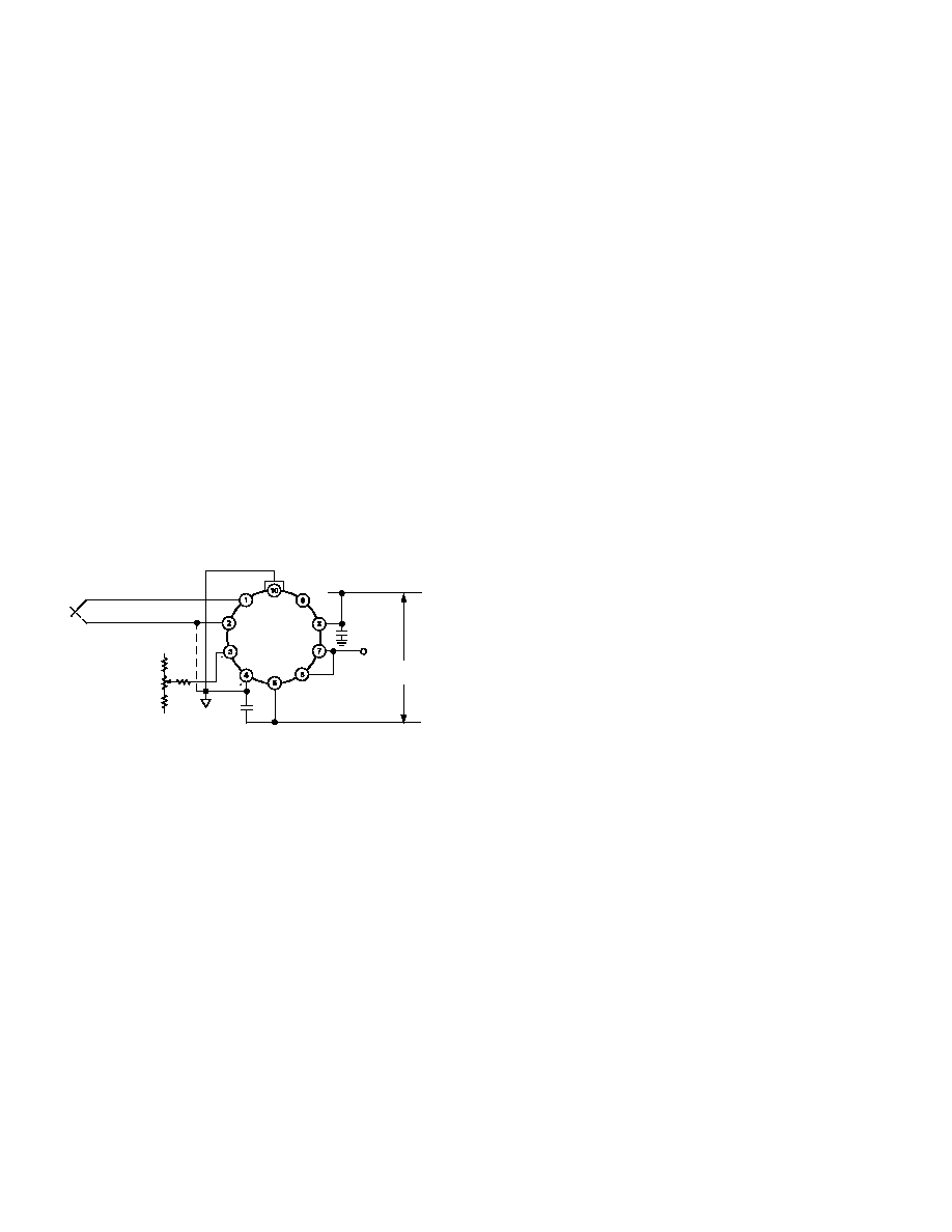
TEMPERATURE PROPORTIONAL OUTPUT MODE
The AD596/AD597 can be used to generate a temperature
proportional output of 10 mV/
°
C when operated with J and K
type thermocouples as shown in Figure 1. Thermocouples pro-
duce low level output voltages which are a function of both the
temperature being measured and the reference or cold junction
temperature. The AD596/AD597 compensates for the cold
junction temperature and amplifies the thermocouple signal to
produce a high level 10 mV/
°
C voltage output which is a func-
tion only of the temperature being measured. The temperature
stability of the part indicates the sensitivity of the output voltage
to changes in ambient or device temperatures. This is typically
0.02
°
C/
°
C over the +25
°
C to +100
°
C recommended ambient
temperature range. The parts will operate over the extended
ambient temperature ranges from 55
°
C to +125
°
C, but ther-
mocouple nonlinearity at the reference junction will degrade the
temperature stability over this extended range. Table I is a list of
ideal AD596/AD597 output voltages as a function of Celsius
temperature for type J and K ANSI standard thermocouples
with package and reference junction at 60
°
C. As is normally the
case, these outputs are subject to calibration and temperature
sensitivity errors. These tables are derived using the ideal trans-
fer functions:
AD596 output = (Type J voltage + 301.5
µ
V)
×
180.57
AD597 output = (Type K voltage)
×
245.46
0.01 F
1M
+15V
15V
100k
10k
100k
CONSTANTAN
(ALUMEL)
IRON
(CHROMEL)
OPTIONAL
OFFSET
ADJUST
0.01 F
V
OUT
+5V TO +30V
0 TO 25V
SPAN OF
+5V TO +30V
AD596/
AD597*
*H PACKAGE PINOUT SHOWN
Figure 1. Temperature Proportional Output Connection
The offsets and gains of these devices have been laser trimmed
to closely approximate thermocouple characteristics over mea-
surement temperature ranges centered around 175
°
C with the
AD596/AD597 at an ambient temperature between 25
°
C and
100
°
C. This eliminates the need for additional gain or offset
adjustments to make the output voltage read:
V
OUT
= 10 mV/
°
C
×
(thermocouple temperature in
°
C) (within
specified tolerances).
Excluding calibration errors, the above transfer function is accu-
rate to within 1
°
C from +80
°
C to +550
°
C for the AD596 and
20
°
C to +350
°
C for the AD597. The different temperature
ranges are due to the differences in J and K type thermocouple
curves.
European DIN FE-CuNi thermocouple vary slightly from ANSI
type J thermocouples. Table I does not apply when these types
of thermocouples are used. The transfer functions given previ-
ously and a thermocouple table should be used instead.
Figure 1 also shows an optional trimming network which can be
used to change the device's offset voltage. Injecting or sinking
200 nA from Pin 3 will offset the output approximately 10 mV
(1
°
C).
The AD596/AD597 can operate from a single supply from 5 V
to 36 V or from split supplies totalling 36 V or less as shown.
Since the output can only swing to within 2 V of the positive
supply, the usable measurement temperature range will be re-
stricted when positive supplies less than 15 V for the AD597
and 10 V for the AD596 are used. If the AD596/AD597 is to be
used to indicate negative Celsius temperatures, then a negative
supply is required.
Common-mode voltages on the thermocouple inputs must
remain within the common-mode voltage range of the AD596/
AD597, with a return path provided for the bias currents. If the
thermocouple is not remotely grounded, then the dotted line
connection shown in Figure 1 must be made to one of the ther-
mocouple inputs. If there is no return path for the bias currents,
the input stage will saturate, causing erroneous output voltages.
In this configuration, the AD596/AD597 H package option has
circuitry which detects the presence of an open thermocouple. If
the thermocouple loop becomes open, one or both of the inputs
to the device will be deprived of bias current causing the output
to saturate. It is this saturation which is detected internally and
used to activate the alarm circuitry. The output of this feature
has a flexible format which can be used to source or sink up to
20 mA of current. The collector (+ALM) should not be allowed
to become more positive than (V
S
+ 36 V), however, it may be
permitted to be more positive than +V
S
. The emitter voltage
(ALM) should be constrained such that it does not become
more positive than 4 V below +V
S
. If the alarm feature is not
used, this pin should be connected to Pins 4 or 5 as shown in
Figure 1. The alarm function is unavailable on the AR package
option.
AD596/AD597
REV. B
5
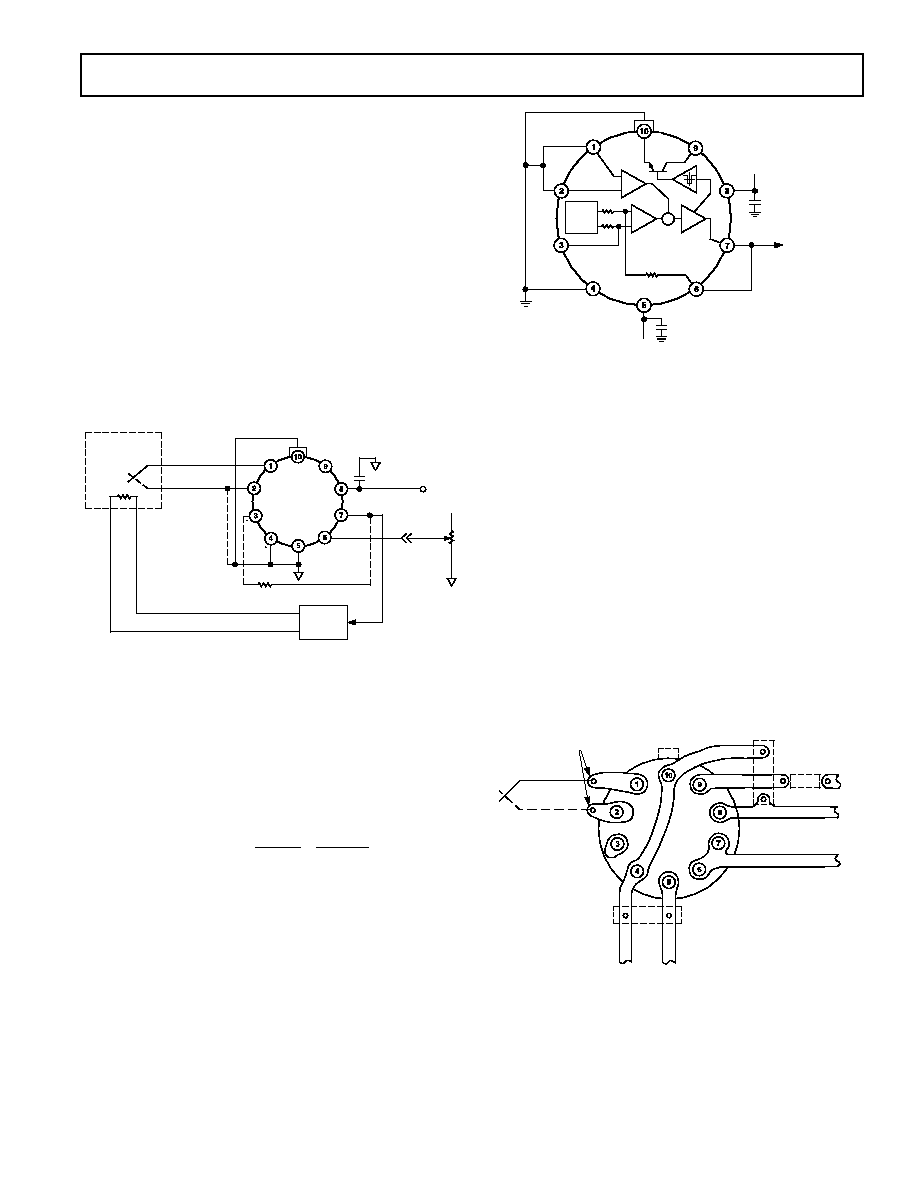
SETPOINT CONTROL MODE
The AD596/AD597 can be connected as a setpoint controller as
shown in Figure 2. The thermocouple voltage is cold junction
compensated, amplified, and compared to an external setpoint
voltage. The relationship between setpoint voltage and tempera-
ture is given in Table I. If the temperature to be controlled is
within the operating range (55
°
C to +125
°
C) of the device, it
can monitor its own temperature by shorting the inputs to
ground. The setpoint voltage with the thermocouple inputs
grounded is given by the expressions:
AD596 Setpoint Voltage =
°
C
×
9.6 mV/
°
C + 42 mV
AD597 Setpoint Voltage =
°
C
×
10.1 mV/
°
C 9.1 mV
The input impedance of the setpoint pin of the AD596/AD597
is approximately 50 k
. The temperature coefficient of this
resistance is
±
15 ppm/
°
C. Therefore, the 100 ppm/
°
C 5 k
pot
shown in Figure 2 will only introduce an additional
±
1
°
C degra-
dation of temperature stability over the +25
°
C to +100
°
C ambi-
ent temperature range.
AD596/
AD597*
CONSTANTAN
(ALUMEL)
IRON
(CHROMEL)
0.01 F
+V
R
HYSTERESIS
(OPTIONAL)
TEMPERATURE
CONTROLLED
REGION
HEATER
DRIVER
TEMPERATURE
COMPARATOR
OUTPUT
SET-
POINT
VOLTAGE
V
REF
5k
100ppm/ C
SET-
POINT
VOLTAGE
*H PACKAGE PINOUT SHOWN
Figure 2. Setpoint Control Mode
Switching hysteresis is often used in setpoint systems of this type
to provide noise immunity and increase system reliability. By
reducing the frequency of on-off cycling, mechanical component
wear is reduced leading to enhanced system reliability. This can
easily be implemented with a single external resistor between
Pins 7 and 3 of the AD596/AD597. Each 200 nA of current
injected into Pin 3 when the output switches will cause about
1
°
C of hysteresis; that is:
R
HYST
(
)
=
V
OUT
200 nA
×
1
°
C
HYST
In the setpoint configuration, the AD596/AD597 output is
saturated at all times, so the alarm transistor will be ON regard-
less of whether there is an open circuit or not. However, ALM
must be tied to a voltage below (+V
S
4 V) for proper operation
of the rest of the circuit.
STAND-ALONE TEMPERATURE TRANSDUCER
The AD596/AD597 may be configured as a stand-alone Celsius
thermometer as shown in Figure 3.
0.01 F
V
S
V
OUT
9.6mV/ C
+V
S
0.01 F
+
G
A
+
ICE
POINT
COMP
+
AD596/
AD597*
+
G
*H PACKAGE PINOUT SHOWN
Figure 3. Stand-Alone Temperature Transducer
Temperature Proportional Output Connection
Simply omit the thermocouple and connect the inputs (Pins 1
and 2) to common. The output will now reflect the compensa-
tion voltage and hence will indicate the AD596/AD597 tem-
perature. In this three terminal, voltage output, temperature
sensing mode, the AD596/AD597 will operate over the full
extended 55
°
C to +125
°
C temperature range. The output
scaling will be 9.6 mV per
°
C with the AD596 and 10.1 mV per
°
C with the AD597. Additionally there will be a 42 mV offset
with the AD596 causing it to read slightly high when used in
this mode.
THERMOCOUPLE CONNECTIONS
The connection of the thermocouple wire and the normal wire
or printed circuit board traces going to the AD596/AD597
forms an effective reference junction as shown in Figure 4. This
junction must be kept at the same temperature as the AD596/
AD597 for the internal cold junction compensation to work
properly. Unless the AD596/AD597 is in a thermally stable
enclosure, the thermocouple leads should be brought in directly
to Pins 1 and 2.
REFERENCE JUNCTION
CONSTANTAN
(ALUMEL)
IRON
(CHROMEL)
NOTE:
A BIAS RETURN PATH
FROM PINS 1 AND 2
OF LESS THAN 1k
IMPEDANCE MUST BE
PROVIDED.
0.01 F
AD596/
AD597*
LIMITING RESISTOR
TO
LED
0.01 F
+V
S
V
OUT
*H PACKAGE PINOUT SHOWN
GND
V
S
Figure 4. PCB Connections
To ensure secure bonding, the thermocouple wire should be
cleaned to remove oxidization prior to soldering. Noncorrosive
resin flux is effective with iron, constantan, chromel, and
alumel, and the following solders: 95% tin5% silver, or 90%
tin10% lead.