AD5680 5 V 18-Bit nanoDAC in a SOT-23 Data Sheet (Rev. 0)
5 V 18-Bit nanoDAC
TM
in a SOT-23
AD5680
Rev. 0
Information furnished by Analog Devices is believed to be accurate and reliable. However, no
responsibility is assumed by Analog Devices for its use, nor for any infringements of patents or other
rights of third parties that may result from its use. Specifications subject to change without notice. No
license is granted by implication or otherwise under any patent or patent rights of Analog Devices.
Trademarks and registered trademarks are the property of their respective owners.
One Technology Way, P.O. Box 9106, Norwood, MA 02062-9106, U.S.A.
Tel: 781.329.4700
www.analog.com
Fax: 781.461.3113
©2006 Analog Devices, Inc. All rights reserved.
FEATURES
Single 18-bit nanoDAC
18-bit monotonic
12-bit accuracy guaranteed
Tiny 8-lead SOT-23 package
Power-on reset to zero scale/midscale
4.5 V to 5.5 V power supply
Serial interface
Rail-to-rail operation
SYNC interrupt facility
Temperature range -40°C to +105°C
APPLICATIONS
Closed-loop process control
Low bandwidth data acquisition systems
Portable battery-powered instruments
Gain and offset adjustment
Precision setpoint control
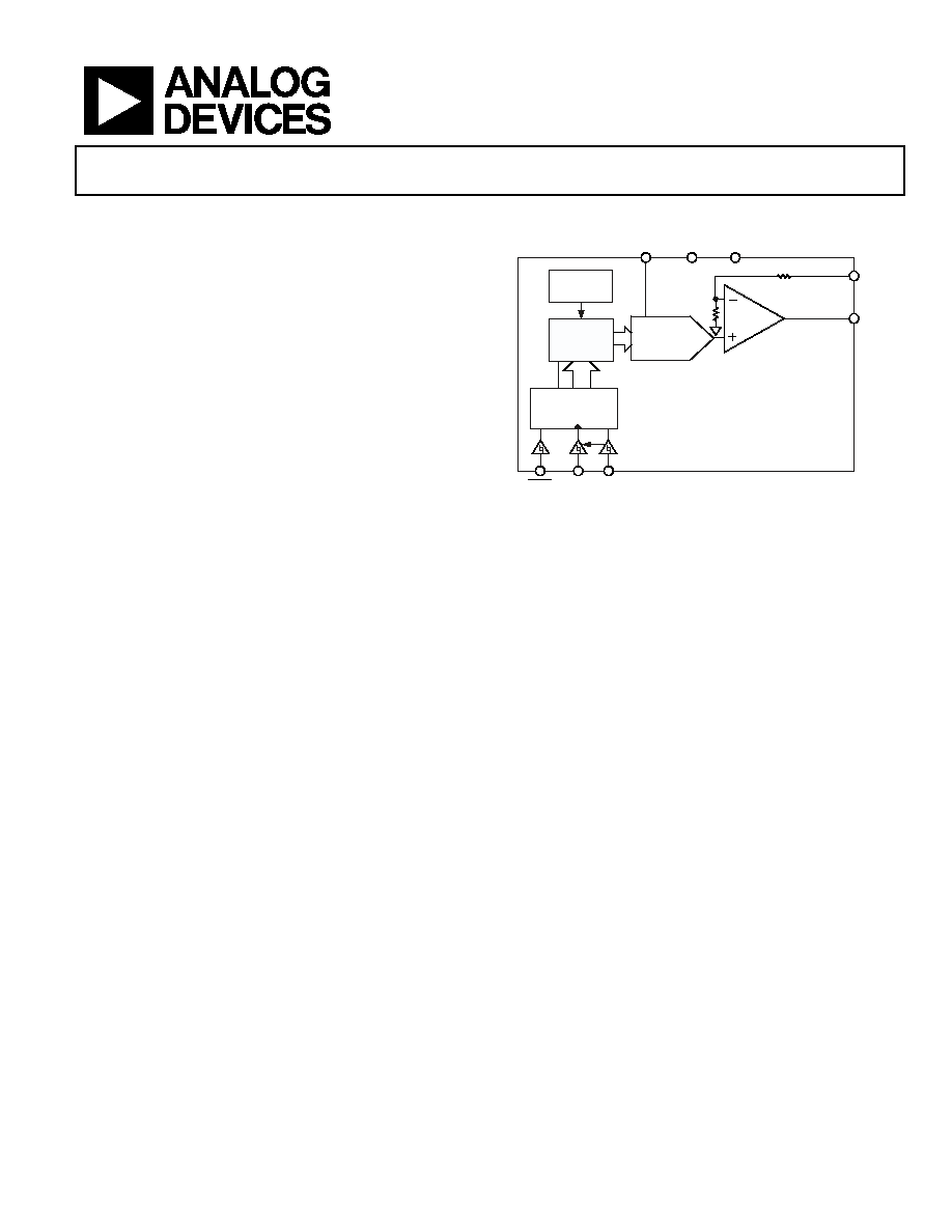
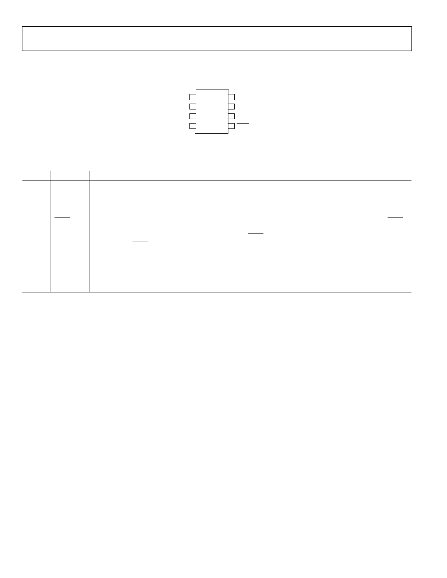
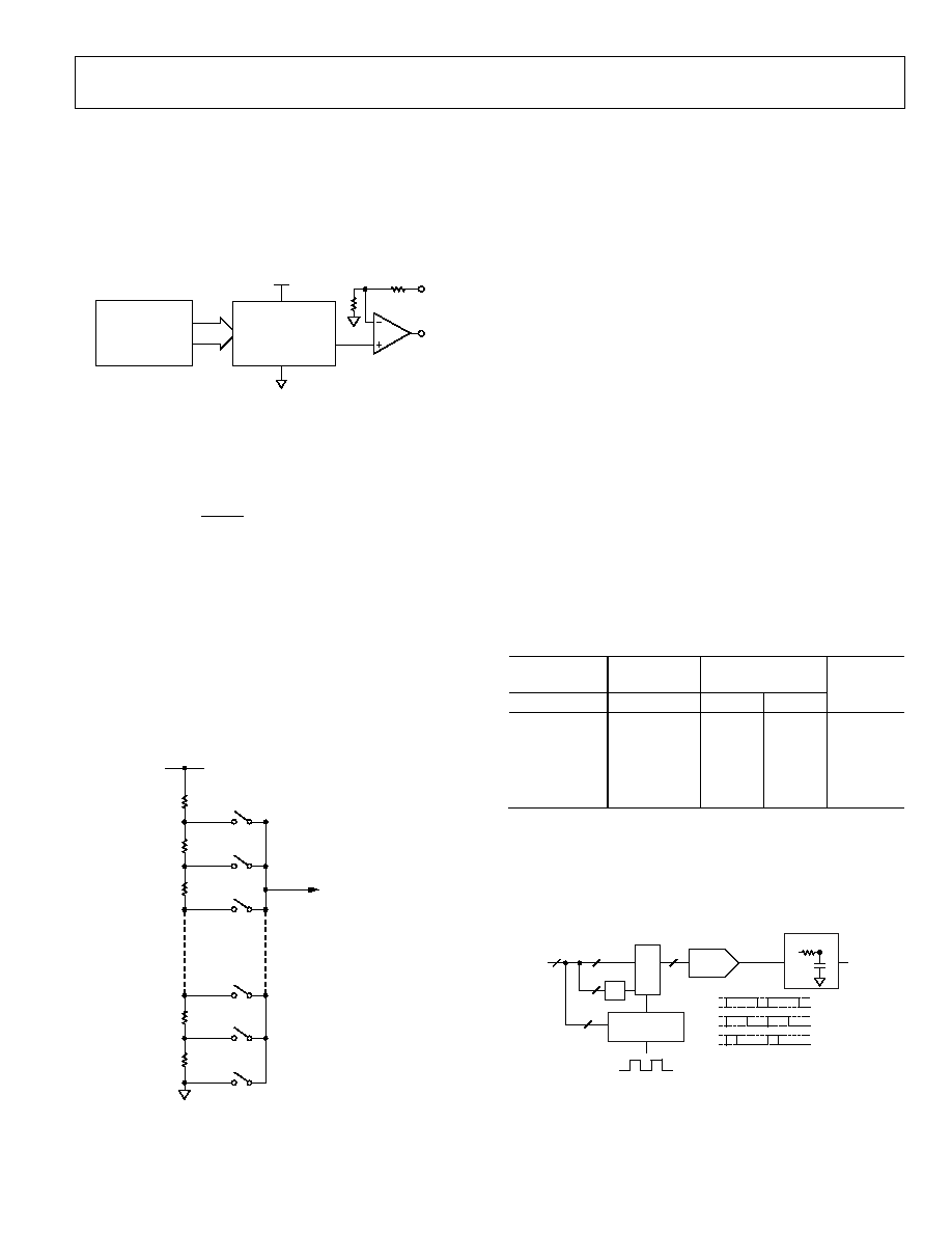
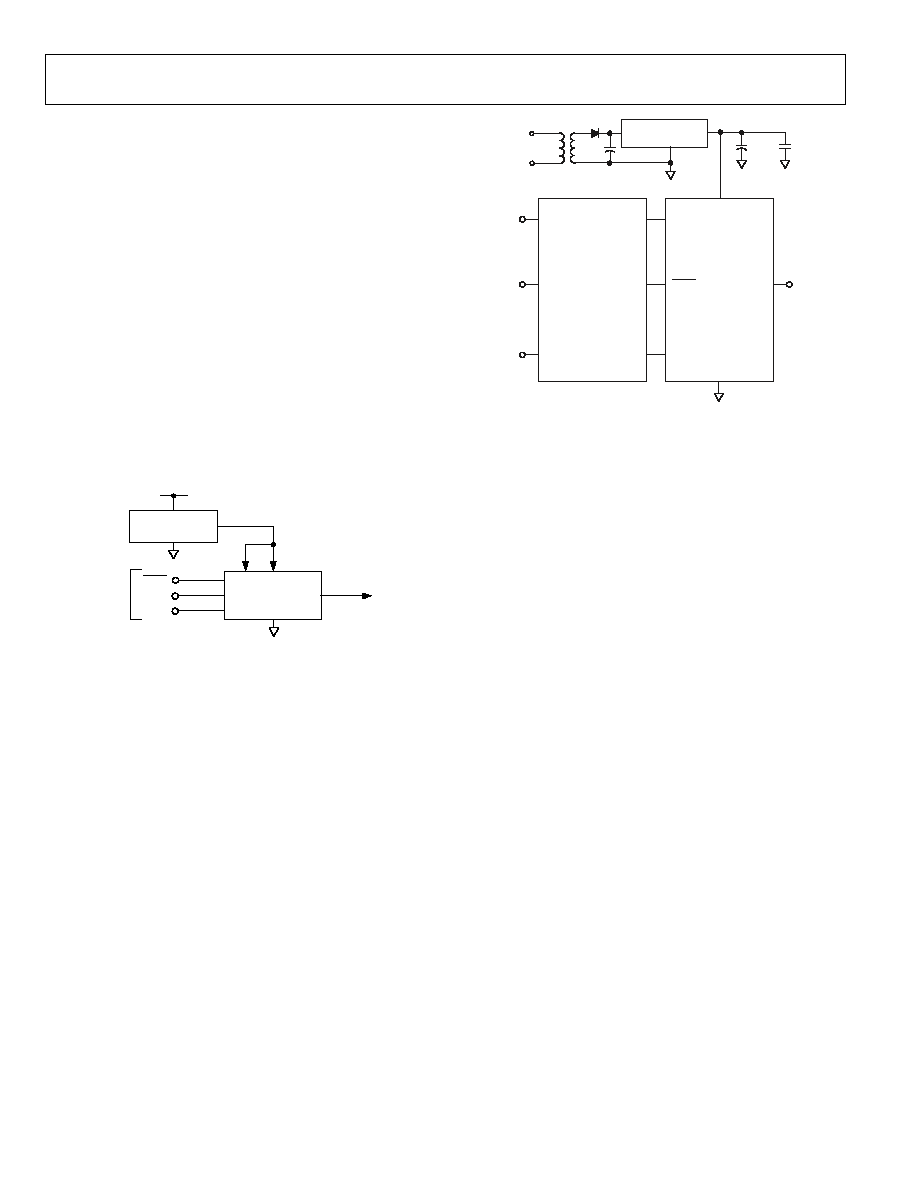
FUNCTIONAL BLOCK DIAGRAM
V
OUT
V
FB
V
DD
GND
V
REF
AD5680
18-BIT
DAC
REF(+)
POWER-ON
RESET
DAC
REGISTER
INPUT
CONTROL
LOGIC
DIN
SCLK
SYNC
058
54-
001
OUTPUT
BUFFER
Figure 1.
GENERAL DESCRIPTION
The AD5680, a member of the nanoDAC family, is a single,
18-bit buffered voltage-out DAC that operates from a single
4.5 V to 5.5 V supply and is 18-bit monotonic.
The AD5680 requires an external reference voltage to set the
output range of the DAC. The part incorporates a power-on
reset circuit that ensures the DAC output powers up to 0 V
(AD5680-1) or to midscale (AD5680-2) and remains there until
a valid write takes place.
The low power consumption of this part in normal operation
makes it ideally suited to portable battery-operated equipment.
The power consumption is 1.6 mW at 5 V.
The AD5680 on-chip precision output amplifier allows rail-to-
rail output swing to be achieved. For remote sensing applications,
the output amplifier's inverting input is available to the user.
The AD5680 uses a versatile 3-wire serial interface that operates
at clock rates up to 30 MHz, and is compatible with standard
SPI®, QSPITM, MICROWIRETM, and DSP interface standards.
PRODUCT HIGHLIGHTS
1.
18 bits of resolution.
2.
12-bit accuracy guaranteed for 18-bit DAC.
3.
Available in an 8-lead SOT-23.
4.
Low power. Typically consumes 1.6 mW at 5 V.
5.
Power-on reset to zero scale or to midscale.
RELATED DEVICES
AD5662
16-bit DAC in SOT-23.

AD5680
Rev. 0 | Page 2 of 20
TABLE OF CONTENTS
Features .............................................................................................. 1
Applications....................................................................................... 1
Functional Block Diagram .............................................................. 1
General Description ......................................................................... 1
Product Highlights ........................................................................... 1
Related Devices ................................................................................. 1
Revision History ............................................................................... 2
Specifications..................................................................................... 3
Timing Characteristics..................................................................... 4
Absolute Maximum Ratings............................................................ 5
ESD Caution.................................................................................. 5
Pin Configuration and Function Description .............................. 6
Typical Performance Characteristics ............................................. 7
Terminology .................................................................................... 10
Theory of Operation ...................................................................... 11
DAC Section................................................................................ 11
Resistor String ............................................................................. 11
Output Amplifier........................................................................ 11
Interpolator Architecture .......................................................... 11
Serial Interface ............................................................................ 12
Input Shift Register .................................................................... 12
SYNC Interrupt .......................................................................... 12
Power-On Reset.......................................................................... 12
Microprocessor Interfacing....................................................... 13
Applications..................................................................................... 14
Closed-Loop Applications ........................................................ 14
Filter ............................................................................................. 14
Choosing a Reference for the AD5680 .................................... 15
Using a Reference as a Power Supply for the AD5680 .......... 16
Using the AD5680 with a Galvanically Isolated Interface .... 16
Power Supply Bypassing and Grounding................................ 16
Outline Dimensions ....................................................................... 17
Ordering Guide .......................................................................... 17
REVISION HISTORY
6/06--Revision 0: Initial Version
AD5680
Rev. 0 | Page 3 of 20
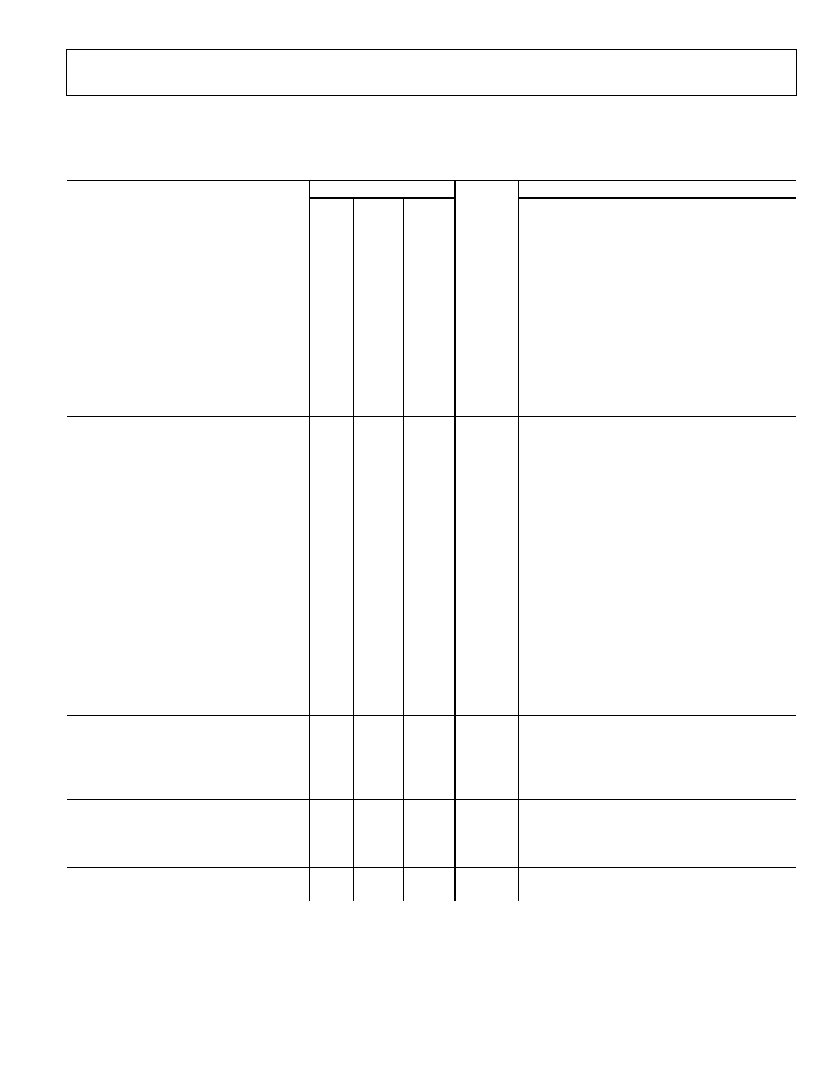
SPECIFICATIONS
V
DD
= 4.5 V to 5.5 V; R
L
= 2 k to GND; C
L
= 200 pF to GND; V
REF
= V
DD
; all specifications T
MIN
to T
MAX
, unless otherwise noted.
Table 1.
B
Grade
B
Version
1
Parameter Min
Typ
Max
Unit
Conditions/Comments
STATIC PERFORMANCE
2
Resolution 18
Bits
Relative Accuracy
±32
±64
LSB
Differential Nonlinearity
3
±1
LSB
Measured in 50 Hz system bandwidth
±2
LSB
Measured in 300 Hz system bandwidth
Zero-Code Error
2
10
mV
All 0s loaded to DAC register
Full-Scale Error
-0.2
-1
% FSR
All 1s loaded to DAC register
Offset Error
±10
mV
Gain Error
±1.5
% FSR
Zero-Code Error Drift
±2
V/°C
Gain Temperature Coefficient
±2.5
ppm
Of FSR/°C
DC Power Supply Rejection Ratio
-100
dB
DAC code = midscale; V
DD
= 5 V ± 10%
OUTPUT CHARACTERISTICS
3
Output Voltage Range
0
V
DD
V
Output Voltage Settling Time
80
85
s
¼ to ¾ scale change settling to ±8 LSB
R
L
= 2 k; 0 pF < C
L
< 200 pF
Slew Rate
1.5
V/s
¼ to ¾ scale
Capacitive Load Stability
2
nF
R
L
=
10
nF
R
L
= 2 k
Output Noise Spectral Density
4
80
nV/Hz
DAC code = midscale, 10 kHz
Output Noise (0.1 Hz to 10 Hz)
4
25
V p-p
DAC code = midscale
Total Harmonic Distortion (THD)
4
-80
dB V
REF
= 2 V ± 300 mV p-p, f = 200 Hz
Digital-to-Analog Glitch Impulse
5
nV-s
1 LSB change around major carry
Digital Feedthrough
0.2
nV-s
DC Output Impedance
0.5
Short-Circuit Current
4
30
mA
V
DD
= 5 V
REFERENCE INPUT
Reference Current
40
75
A
V
REF
= V
DD
= 5 V
Reference Input Range
5
0.75
V
DD
V
Reference Input Impedance
125
k
LOGIC INPUTS
Input Current
±2
A
All digital inputs
V
INL
, Input Low Voltage
0.8
V
V
DD
= 5 V
V
INH
, Input High Voltage
2
V
V
DD
= 5 V
Pin Capacitance
3
pF
POWER REQUIREMENTS
V
DD
4.5
5.5
V
All digital inputs at 0 V or V
DD
I
DD
(Normal Mode)
DAC active and excluding load current
V
DD
= 4.5 V to 5.5 V
325
450
A
V
IH
= V
DD
and V
IL
= GND
POWER EFFICIENCY
I
OUT
/I
DD
85
% I
LOAD
= 2 mA, V
DD
= 5 V
1
Temperature range for B version is -40°C to +105°C, typical at +25°C.
2
DC specifications tested with the outputs unloaded, unless otherwise stated. Linearity calculated using a reduced code range of 2048 to 260096.
3
Guaranteed by design and characterization; not production tested.
4
Output unloaded.
5
Reference input range at ambient where maximum DNL specification is achievable.
AD5680
Rev. 0 | Page 4 of 20
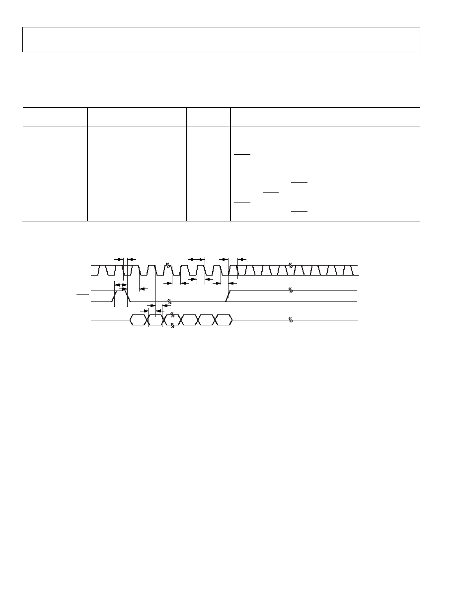
TIMING CHARACTERISTICS
All input signals are specified with tr = tf = 1 ns/V (10% to 90% of V
DD
) and timed from a voltage level of (V
IL
+ V
IH
)/2. See Figure 2.
V
DD
= 4.5 V to 5.5 V; all specifications T
MIN
to T
MAX
, unless otherwise noted.
Table 2.
Limit
at
T
MIN
, T
MAX
Parameter V
DD
= 4.5 V to 5.5 V
Unit
Conditions/Comments
t
1
1
33
ns min
SCLK cycle time
t
2
13
ns min
SCLK high time
t
3
13
ns min
SCLK low time
t
4
13 ns
min
SYNC to SCLK falling edge setup time
t
5
5
ns min
Data setup time
t
6
4.5
ns min
Data hold time
t
7
0 ns
min
SCLK falling edge to SYNC rising edge
t
8
33 ns
min
Minimum SYNC high time
t
9
13 ns
min
SYNC rising edge to SCLK fall ignore
t
10
0 ns
min
SCLK falling edge to SYNC fall ignore
1
Maximum SCLK frequency is 30 MHz at V
DD
= 4.5 V to 5.5 V.
DIN
SYNC
SCLK
DB23
DB0
t
9
t
10
t
4
t
3
t
2
t
7
t
6
t
5
t
1
t
8
05
85
4-
00
2
Figure 2. Serial Write Operation
AD5680
Rev. 0 | Page 5 of 20
ABSOLUTE MAXIMUM RATINGS
T
A
= 25°C, unless otherwise noted.
Table 3.
Parameter Rating
V
DD
to GND
-0.3 V to +7 V
V
OUT
to GND
-0.3 V to V
DD
+ 0.3 V
V
FB
to GND
-0.3 V to V
DD
+ 0.3 V
V
REF
to GND
-0.3 V to V
DD
+ 0.3 V
Digital Input Voltage to GND
-0.3 V to V
DD
+ 0.3 V
Operating Temperature Range
Industrial (B Version)
-40°C to +105°C
Storage Temperature Range
-65°C to +150°C
Junction Temperature (T
J
max) 150°C
Power Dissipation
(T
J
max - T
A
)/
JA
SOT-23 Package (4-Layer Board)
JA
Thermal Impedance
119°C/W
Reflow Soldering Peak Temperature
Pb-free
260°C
Stresses above those listed under Absolute Maximum Ratings
may cause permanent damage to the device. This is a stress
rating only; functional operation of the device at these or any
other conditions above those indicated in the operational
section of this specification is not implied. Exposure to absolute
maximum rating conditions for extended periods may affect
device reliability.
ESD CAUTION
ESD (electrostatic discharge) sensitive device. Electrostatic charges as high as 4000 V readily accumulate on the
human body and test equipment and can discharge without detection. Although this product features
proprietary ESD protection circuitry, permanent damage may occur on devices subjected to high energy
electrostatic discharges. Therefore, proper ESD precautions are recommended to avoid performance
degradation or loss of functionality.
AD5680
Rev. 0 | Page 6 of 20
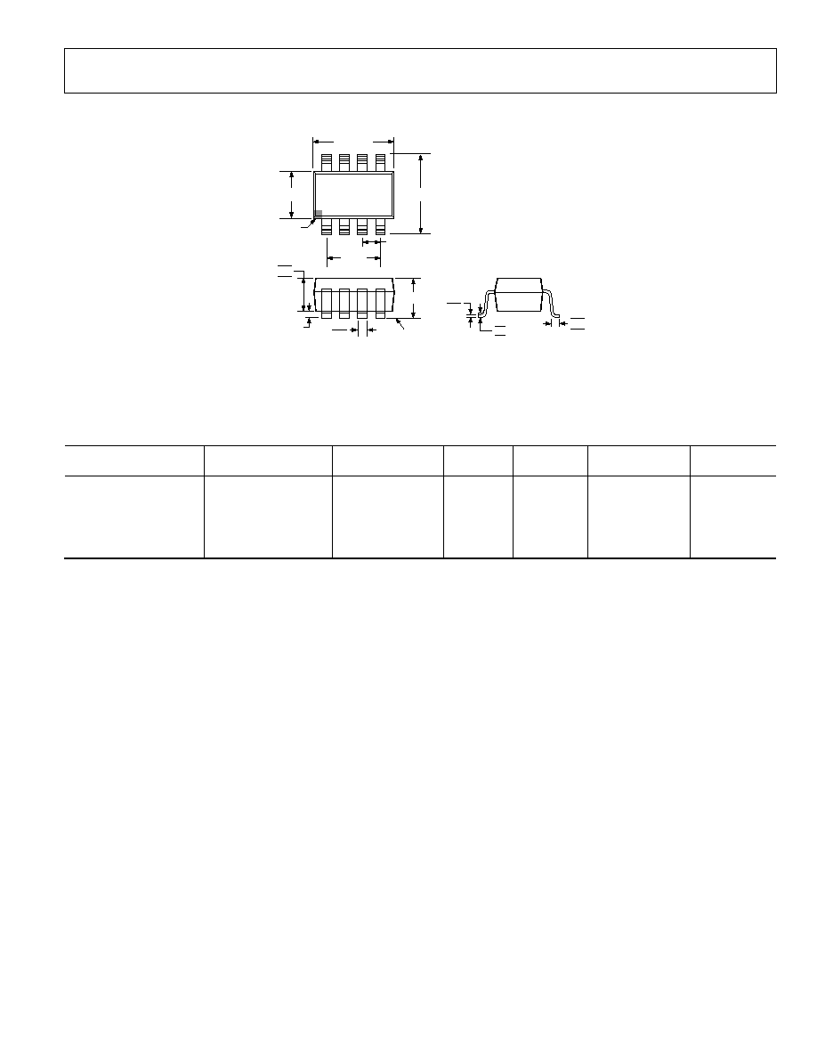
PIN CONFIGURATION AND FUNCTION DESCRIPTION
V
DD
1
V
REF
2
V
FB
3
V
OUT
4
GND
8
DIN
7
SCLK
6
SYNC
5
AD5680
TOP VIEW
(Not to Scale)
05
85
4-
0
03
Figure 3. Pin Configuration
Table 4. Pin Function Descriptions
Pin No. Mnemonic Function
1 V
DD
Power Supply Input. The part can be operated from 4.5 V to 5.5 V. V
DD
should be decoupled to GND.
2 V
REF
Reference Voltage Input.
3 V
FB
Feedback Connection for the Output Amplifier. V
FB
should be connected to V
OUT
for normal operation.
4 V
OUT
Analog Output Voltage from DAC. The output amplifier has rail-to-rail operation.
5
SYNC
Level-Triggered Control Input (Active Low). This is the frame synchronization signal for the input data. When SYNC
goes low, it enables the input shift register and data is transferred in on the falling edges of the following clocks.
The DAC is updated following the 24
th
clock cycle unless SYNC is taken high before this edge, in which case the
rising edge of SYNC acts as an interrupt and the write sequence is ignored by the DAC.
6 SCLK
Serial Clock Input. Data is clocked into the input shift register on the falling edge of the serial clock input. Data can
be transferred at rates up to 30 MHz.
7 DIN
Serial Data Input. This device has a 24-bit shift register. Data is clocked into the register on the falling edge of the
serial clock input.
8
GND
Ground Reference Point (for all circuitry on the part).
AD5680
Rev. 0 | Page 7 of 20
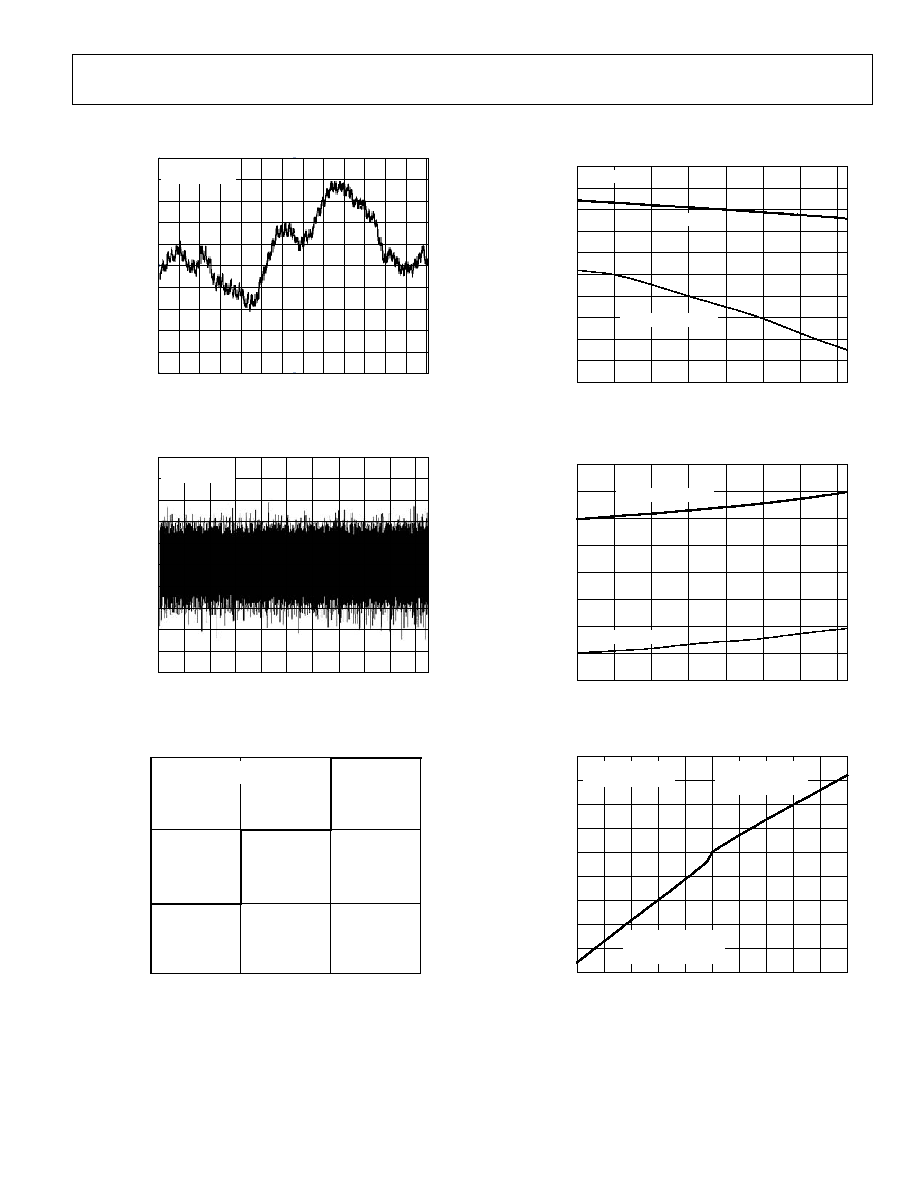
TYPICAL PERFORMANCE CHARACTERISTICS
CODE
I
N
L
ER
R
O
R
(
L
SB
)
40
16
24
32
0
8
24
40
32
8
16
0
40k
80k
120k
160k
200k
240k
05
854
-
02
8
V
DD
= V
REF
= 5V
T
A
= 25°C
Figure 4. Typical INL Plot
CODE
D
N
L
E
RRO
R
(
L
S
B)
1.0
0.6
0.4
0.2
0.8
0
0.4
0.2
0.6
1.0
0.8
0
25k
50k
100k
75k
125k 150k
225k
200k
175k
250k
05
854
-
02
9
V
DD
= V
REF
= 5V
T
A
= 25°C
Figure 5. Typical DNL Plot in 50 Hz System Bandwidth
SYSTEM BANDWIDTH (Hz)
0
0
D
N
L
(
L
S
B
)
50
300
>300
±4
±1
±2
V
DD
= 4.5V TO 5.5V
T = 40°C TO +105°C
05
85
4-
0
42
Figure 6. DNL Performance vs. System Bandwidth
TEMPERATURE (
°C)
E
RRO
R (
%
F
S
R)
0
0.04
0.02
0.06
0.08
0.01
0.18
0.16
0.14
0.12
0.20
40
20
40
20
0
100
80
60
05
30
2
-
02
3
V
DD
= 5V
GAIN ERROR
FULL-SCALE ERROR
Figure 7. Gain Error and Full-Scale Error vs. Temperature
TEMPERATURE (
°C)
E
R
RO
R (
m
V
)
1.5
1.0
0.5
0
2.0
1.5
1.0
0.5
2.5
40
20
40
20
0
8
60
100
05
30
2
-
02
4
0
OFFSET ERROR
ZERO-SCALE ERROR
Figure 8. Zero-Scale Error and Offset Error vs. Temperature
I (mA)
E
RRO
R V
O
L
T
AG
E
(
V
)
0.20
0.25
0.20
0.15
0.10
0.05
0
0.05
0.10
0.15
5
4
3
2
1
0
1
2
4
3
5
0
585
4-
0
14
V
DD
= V
REF
= 5V, 3V
T
A
= 25
°C
DAC LOADED WITH
ZERO SCALE
SINKING CURRENT
DAC LOADED WITH
FULL SCALE
SOURCING CURRENT
Figure 9. Headroom at Rails vs. Source and Sink Current
AD5680
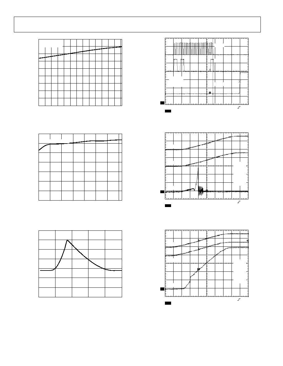
Rev. 0 | Page 8 of 20
450
0
CODE
I
DD
(µ
A
)
05
85
4-
0
07
0
50
100
150
200
250
300
350
400
4000
8000
12000
16000
20000
24000
V
DD
= V
REF
= 5V
T
A
= 25°C
Figure 10. Supply Current vs. Code
350
0
TEMPERATURE (°C)
I
DD
(µ
A
)
05
85
4-
0
06
50
100
150
200
250
300
40
20
0
20
40
60
80
100
V
DD
= V
REF
= 5V
Figure 11. Supply Current vs. Temperature
700
0
100
0
5
V
LOGIC
(V)
I
DD
(µ
A
)
05
85
4-
0
04
200
300
400
500
600
1
2
3
4
V
DD
= 5V
T
A
= 25°C
Figure 12. Supply Current vs. Logic Input Voltage
05
85
4-
01
5
CH1 2.00V
CH3
1.00V
CH2 2.00V
M 20.0µs
CH4 1.30V
3
SCLK
D
IN
V
OUT
1
2
: 1.52V
: 64.8µs
@: 1.20V
Figure 13. Full-Scale Settling Time, 5 V
05
85
4-
01
6
CH1 3.00V
CH3
100mV
CH2 3.00V
M 100µs
CH1 2.40V
3
V
DD
1
2
V
REF
V
OUT
V
OUT
C3 MAX
284mV
V
OUT
C3 MIN
52mV
Figure 14. Power-On Reset to 0 V
05
85
4-
01
7
CH1 3.00V
CH3
500mV
CH2 3.00V
M 100µs
CH1 2.40V
3
V
DD
1
2
V
REF
V
OUT
V
OUT
C3 MAX
2.5V
V
OUT
C3 MIN
40mV
Figure 15. Power-On Reset to Midscale
AD5680
Rev. 0 | Page 9 of 20
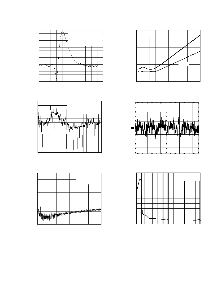
SAMPLE NUMBER
AM
P
L
I
T
UD
E
2.502500
2.502250
2.502000
2.501750
2.501500
2.501250
2.501000
2.500750
2.500500
2.500250
2.500000
2.499750
2.499500
2.499250
2.499000
2.498750
0
150 200 250
50
100
300
350 400 450 500 550
05
85
4-
0
05
V
DD
= V
REF
= 5V
T
A
= 25
°C
13nS/SAMPLE NUMBER
1 LSB CHANGE AROUND
MIDSCALE (0x20000 TO 0x1FFFF)
GLITCH IMPULSE = 2.723nV.s
Figure 16. Digital-to-Analog Glitch Impulse (Negative)
SAMPLES × 6.5ns
AM
P
L
I
T
UDE
2.5010
2.4986
0
058
54
-
02
0
2.4988
2.4990
2.4992
2.4994
2.4996
2.4998
2.5000
2.5002
2.5004
2.5006
2.5008
50
100
150
200
250
300
350
400
450
500
V
DD
= V
REF
= 5V
T
A
= 25°C
DAC LOADED WITH MIDSCALED
DIGITAL
FEEDTHROUGH = 0.201nV
Figure 17. Digital Feedthrough
FREQUENCY (kHz)
(d
B
)
20
100
0
10
05
85
4-
01
8
30
40
50
60
70
80
90
1
2
3
4
5
6
7
8
9
V
DD
= 5V
T
A
= 25°C
FULLSCALE LOADED
V
REF
= 2V ±300mV p-p
0
Figure 18. Total Harmonic Distortion
CAPACITANCE (nF)
TI
M
E
(
µ
s
)
16
14
12
10
8
6
4
0
1
2
3
4
5
6
7
9
8
1
05
85
4-
0
27
V
REF
= V
DD
T
A
= 25
°C
V
DD =
5V
V
DD =
3V
Figure 19. Settling Time vs. Capacitive Load
05
85
4
-
01
9
5s/DIV
5µ
V/
D
I
V
1
V
DD
= V
REF
= 5V
T
A
= 25°C
DAC LOADED WITH MIDSCALE
V
REF
Figure 20. 0.1 Hz to 10 Hz Output Noise Plot
FREQUENCY (Hz)
N
O
I
S
E (
n
V/
Hz
)
1000
0
100
1M
0
585
4-
0
13
1k
10k
100k
V
DD
= V
REF
= 5V
T
A
= 25°C
MIDSCALE LOADED
900
800
700
600
500
400
300
200
100
Figure 21. Noise Spectral Density

AD5680
Rev. 0 | Page 10 of 20
TERMINOLOGY
Relative Accuracy or Integral Nonlinearity (INL)
For the DAC, relative accuracy or integral nonlinearity is a
measurement of the maximum deviation, in LSBs, from a
straight line passing through the endpoints of the DAC transfer
function. Figure 4 shows a typical INL vs. code plot.
Differential Nonlinearity (DNL)
Differential nonlinearity is the difference between the measured
change and the ideal 1 LSB change between any two adjacent
codes. A specified differential nonlinearity of ±1 LSB maximum
ensures monotonicity. Figure 5 shows a typical DNL vs. code plot.
Zero-Code Error
Zero-code error is a measurement of the output error when
zero code (0x00000) is loaded to the DAC register. Ideally, the
output should be 0 V. The zero-code error is always positive in
the AD5680 because the output of the DAC cannot go below
0 V. It is due to a combination of the offset errors in the DAC
and the output amplifier. Zero-code error is expressed in mV. A
plot of zero-code error vs. temperature can be seen in Figure 7.
Full-Scale Error
Full-scale error is a measurement of the output error when full-
scale code (0x3FFFF) is loaded to the DAC register. Ideally, the
output should be V
DD
- 1 LSB. Full-scale error is expressed in
percent of full-scale range.
Gain Error
This is a measure of the span error of the DAC. It is the deviation
in slope of the DAC transfer characteristic from ideal expressed
as a percent of the full-scale range.
Zero-Code Error Drift
This is a measurement of the change in zero-code error with a
change in temperature. It is expressed in V/°C.
Gain Temperature Coefficient
This is a measurement of the change in gain error with changes
in temperature. It is expressed in (ppm of full-scale range)/°C.
Offset Error
Offset error is a measure of the difference between V
OUT
(actual)
and V
OUT
(ideal) expressed in mV in the linear region of the
transfer function. Offset error is measured on the AD5680 with
Code 2048 loaded in the DAC register.
It can be negative or
positive.
DC Power Supply Rejection Ratio (PSRR)
This indicates how the output of the DAC is affected by
changes in the supply voltage. PSRR is the ratio of the change in
V
OUT
to a change in V
DD
for full-scale output of the DAC. It is
measured in dB. V
REF
is held at 2 V, and V
DD
is varied by ±10%.
Output Voltage Settling Time
This is the amount of time it takes for the output of a DAC to
settle to a specified level for a ¼ to ¾ full-scale input change
and is measured from the 24
th
falling edge of SCLK.
Digital-to-Analog Glitch Impulse
Digital-to-analog glitch impulse is injected into the analog
output when the input code in the DAC register changes state.
It is normally specified as the area of the glitch in nV-s, and is
measured when the digital input code is changed by 1 LSB at
the major carry transition (0x1FFFF to 0x20000). See Figure 16.
Digital Feedthrough
Digital feedthrough is a measure of the impulse injected into
the analog output of the DAC from the digital inputs of the
DAC, but is measured when the DAC output is not updated. It
is specified in nV-s and measured with a full-scale code change
on the data bus, that is, from all 0s to all 1s and vice versa.
Total Harmonic Distortion (THD)
This is the difference between an ideal sine wave and its
attenuated version using the DAC. The sine wave is used as the
reference for the DAC. The THD is a measurement of the
harmonics present on the DAC output. It is measured in dB.
Noise Spectral Density
This is a measurement of the internally generated random
noise. Random noise is characterized as a spectral density
(voltage per Hz). It is measured by loading the DAC to
midscale and measuring noise at the output. It is measured in
nV/Hz. Figure 21 shows a plot of noise spectral density.
AD5680
Rev. 0 | Page 11 of 20
THEORY OF OPERATION
DAC SECTION
The AD5680 DAC is fabricated on a CMOS process. The
architecture consists of a string DAC followed by an output
buffer amplifier. Figure 22 shows a block diagram of the DAC
architecture.
V
DD
R
R
V
OUT
GND
RESISTOR
STRING
REF (+)
REF ()
OUTPUT
AMPLIFIER
DAC REGISTER
05
85
4-
0
3
0
V
FB
Figure 22. DAC Architecture
Because the input coding to the DAC is straight binary, the ideal
output voltage is given by
×
=
262144
D
V
V
REF
OUT
where D is the decimal equivalent of the binary code that is
loaded to the DAC register. It can range from 0 to 262143.
RESISTOR STRING
The resistor string section is shown in Figure 23. It is simply a
string of resistors, each of value R. The code loaded to the DAC
register determines at which node on the string the voltage is
tapped off to be fed into the output amplifier. The voltage is
tapped off by closing one of the switches connecting the string
to the amplifier. Because it is a string of resistors, it is guaranteed
monotonic.
R
R
R
R
R
TO OUTPUT
AMPLIFIER
05
85
4-
03
1
Figure 23. Resistor String
OUTPUT AMPLIFIER
The output buffer amplifier can generate rail-to-rail voltages on
its output, which gives an output range of 0 V to V
DD
. This output
buffer amplifier has a gain of 2 derived from a 50 k resistor
divider network in the feedback path. The output amplifier's
inverting input is available to the user, allowing for remote
sensing. This V
FB
pin must be connected to V
OUT
for normal
operation. It can drive a load of 2 k in parallel with 1000 pF to
GND. The source and sink capabilities of the output amplifier can
be seen in Figure 9. The slew rate is 1.5 V/s with a ¼ to ¾ full-
scale settling time of 10 s.
INTERPOLATOR ARCHITECTURE
The AD5680 contains a 16-bit DAC with an internal clock
generator and interpolator. The voltage levels generated by the
16-bit, 1 LSB step can be subdivided using the interpolator to
increase the resolution to 18 bits.
The 18-bit input code can be divided into two segments:
16-bit DAC code (DB19 to DB4) and 2-bit interpolator code
(DB3 and DB2). The input to the DAC is switched between a
16-bit code (for example, Code 1023) and a 16-bit code + 1 LSB
(for example, Code 1024). The 2-bit interpolator code deter-
mines the duty cycle of the switching and hence the 18-bit
code level. See Table 5 for an example.
Table 5.
18-Bit Code
16-Bit
DAC Code
2-Bit
Interpolator Code
DB19 to DB2
DB19 to DB4
DB3
DB2
Duty Cycle
4092 1023 0
0
0
4093 1023 0
1
25%
4094 1023 1
0
50%
4095 1023 1
1
75%
4096 1024 0
0
0
The DAC output voltage is given by the average value of
the waveform switching between 16-bit code (C) and 16-bit
code + 1 (C + 1). The output voltage is a function of the duty
cycle of the switching.
05854-
032
C
2
16
16
18
+1
C
C
C
PLANT
DAC
V
OUT
FILTER
18-BIT INPUT CODE
MUX
C + 1
CLK
INTERPOLATOR
75% DUTY CYCLE
50% DUTY CYCLE
25% DUTY CYCLE
C + 1
C + 1
C + 1
Figure 24. Interpolation Architecture
AD5680
Rev. 0 | Page 12 of 20
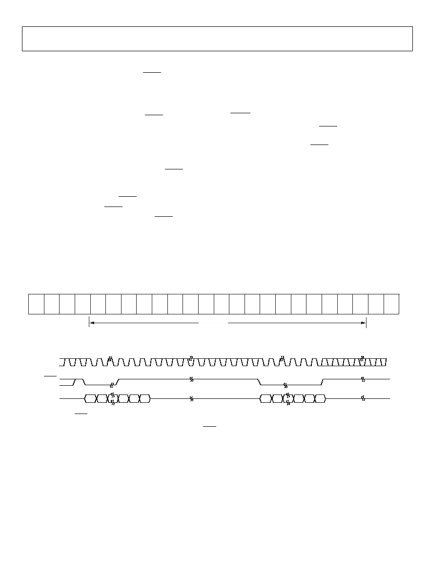
SERIAL INTERFACE
The AD5680 has a 3-wire serial interface (SYNC, SCLK, and
DIN) that is compatible with SPI, QSPI, and MICROWIRE
interface standards as well as with most DSPs. See Figure 2 for
a timing diagram of a typical write sequence.
The write sequence begins by bringing the SYNC line low. Data
from the DIN line is clocked into the 24-bit shift register on the
falling edge of SCLK. The serial clock frequency can be as high
as 30 MHz, making the AD5680 compatible with high speed
DSPs. On the 24
th
falling clock edge, the last data bit is clocked
in and the programmed function is executed, that is, a change
in DAC register contents occurs. At this stage, the SYNC line
can be kept low or be brought high. In either case, it must be
brought high for a minimum of 33 ns before the next write
sequence so that a falling edge of SYNC can initiate the next
write sequence. Because the SYNC buffer draws more current
when V
IN
= 2 V than it does when V
IN
= 0.8 V, SYNC should be
idled low between write sequences for even lower power
operation. As mentioned previously it must, however, be
brought high again just before the next write sequence.
INPUT SHIFT REGISTER
The input shift register is 24 bits wide (see Figure 25). The first
four bits are don't care bits. The next 18 bits are the data bits
followed by two don't care bits. These are transferred to the
DAC register on the 24
th
falling edge of SCLK.
SYNC INTERRUPT
In a normal write sequence, the SYNC line is kept low for at
least 24 falling edges of SCLK, and the DAC is updated on the
24
th
falling edge. However, if SYNC is brought high before the
24
th
falling edge, this acts as an interrupt to the write sequence.
The shift register is reset and the write sequence is seen as
invalid. Neither an update of the DAC register contents nor a
change in the operating mode occurs (see Figure 26).
POWER-ON RESET
The AD5680 family contains a power-on reset circuit that
controls the output voltage during power-up. The AD5680-1
DAC output powers up to 0 V, and the AD5680-2 DAC output
powers up to midscale. The output remains there until a valid
write sequence is made to the DAC. This is useful in
applications where it is important to know the output state of
the DAC while it is in the process of powering up.
05
85
4-
03
3
X
X
X
X
X
X
D17
D16
D15
D14
D13
D12
D11
D10
D9
D8
D7
D6
D5
D4
D3
D2
D1
D0
DATA BITS
DB23 (MSB)
DB0 (LSB)
Figure 25. Input Register Contents
05
85
4-
03
4
DIN
DB23
DB23
DB0
DB0
INVALID WRITE SEQUENCE:
SYNC HIGH BEFORE 24
TH
FALLING EDGE
VALID WRITE SEQUENCE, OUTPUT UPDATES
ON THE 24
TH
FALLING EDGE
SYNC
SCLK
Figure 26. SYNC Interrupt Facility
AD5680
Rev. 0 | Page 13 of 20
MICROPROCESSOR INTERFACING
AD5680 to Blackfin® ADSP-BF53x Interface
Figure 27 shows a serial interface between the AD5680 and
the Blackfin ADSP-BF53x microprocessor. The ADSP-BF53x
processor family incorporates two dual-channel synchronous
serial ports, SPORT1 and SPORT0, for serial and multiprocessor
communications. Using SPORT0 to connect to the AD5680, the
setup for the interface is as follows. DT0PRI drives the DIN pin
of the AD5680, while TSCLK0 drives the SCLK of the part. The
SYNC is driven from TFS0.
AD5680*
*ADDITIONAL PINS OMITTED FOR CLARITY
TFS0
DTOPRI
TSCLK0
SYNC
DIN
SCLK
0
585
4-
0
35
ADSP-BF53x*
Figure 27. AD5680 to Blackfin ADSP-BF53x Interface
AD5680 to 68HC11/68L11 Interface
Figure 28 shows a serial interface between the AD5680 and the
68HC11/68L11 microcontroller. SCK of the 68HC11/68L11
drives the SCLK of the AD5680, while the MOSI output drives
the serial data line of the DAC.
The SYNC signal is derived from a port line (PC7). The setup
conditions for correct operation of this interface are as follows.
The 68HC11/68L11 is configured with its CPOL bit as 0 and its
CPHA bit as 1. When data is being transmitted to the DAC, the
SYNC line is taken low (PC7). When the 68HC11/68L11 is
configured this way, data appearing on the MOSI output is valid
on the falling edge of SCK. Serial data from the 68HC11/68L11
is transmitted in 8-bit bytes with only eight falling clock edges
occurring in the transmit cycle. Data is transmitted MSB first. To
load data to the AD5680, PC7 is left low after the first eight bits
are transferred, and a second serial write operation is performed
to the DAC; PC7 is taken high at the end of this procedure.
AD5680*
*ADDITIONAL PINS OMITTED FOR CLARITY
PC7
SCK
MOSI
SYNC
SCLK
DIN
05
85
4-
0
36
68HC11/68L11*
Figure 28. AD5680 to 68HC11/68L11 Interface
AD5680 to 80C51/80L51 Interface
Figure 29 shows a serial interface between the AD5680 and the
80C51/80L51 microcontroller. The setup for the interface is as
follows. TxD of the 80C51/80L51 drives SCLK of the AD5680,
while RxD drives the serial data line of the part. The SYNC
signal is again derived from a bit-programmable pin on the port.
In this case, port line P3.3 is used. When data is to be transmitted
to the AD5680, P3.3 is taken low. The 80C51/80L51 transmits
data in 8-bit bytes only; thus only eight falling clock edges occur
in the transmit cycle. To load data to the DAC, P3.3 is left low
after the first eight bits are transmitted, and a second write cycle
is initiated to transmit the second byte of data. P3.3 is taken
high following the completion of this cycle. The 80C51/80L51
outputs the serial data in a format that has the LSB first. The
AD5680 must receive data with the MSB first. The 80C51/80L51
transmit routine should take this into account.
80C51/80L51*
AD5680*
*ADDITIONAL PINS OMITTED FOR CLARITY
P3.3
TxD
RxD
SYNC
SCLK
DIN
0
585
4-
0
37
Figure 29. AD5680 to 80C51/80L51 Interface
AD5680 to MICROWIRE Interface
Figure 30 shows an interface between the AD5680 and any
MICROWIRE-compatible device. Serial data is shifted out on
the falling edge of the serial clock and is clocked into the AD5680
on the rising edge of the SK.
MICROWIRE*
AD5680*
*ADDITIONAL PINS OMITTED FOR CLARITY
CS
SK
SO
SYNC
SCLK
DIN
0
585
4-
0
38
Figure 30. AD5680 to MICROWIRE Interface
AD5680
Rev. 0 | Page 14 of 20
APPLICATIONS
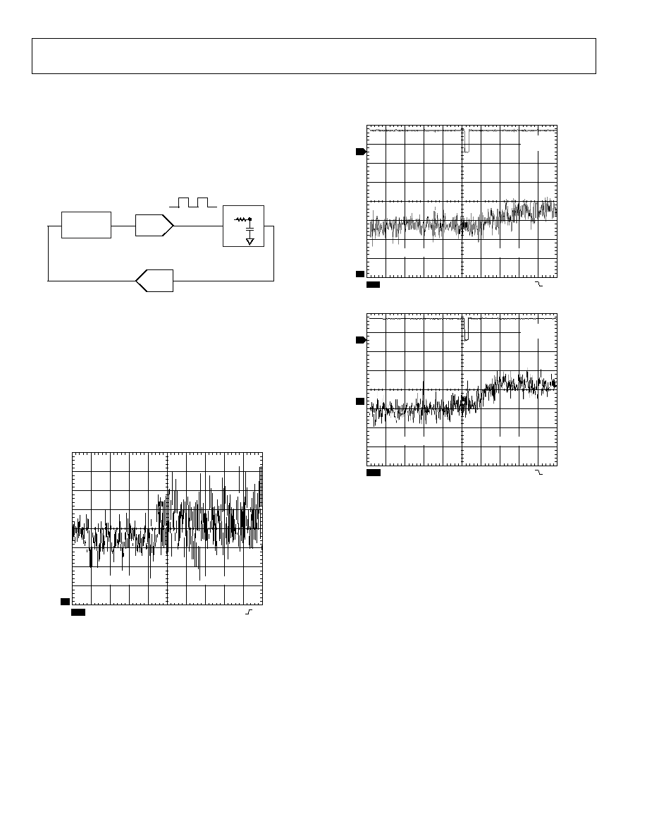
CLOSED-LOOP APPLICATIONS
The AD5680 is suitable for closed-loop low bandwidth
applications. Ideally, the system bandwidth acts as a filter on the
DAC output. (See the Filter section for details of the DAC
output prefiltering and postfiltering.) The DAC updates at the
interpolation frequency of 10 kHz.
05
85
4-
0
39
CONTROLLER
PLANT
ADC
DAC
Figure 31. Typical Closed-Loop Application
FILTER
The DAC output voltage for code transition 4092 to 4094 can be
seen in Figure 32. This is the DAC output unfiltered. Code 4092
does not have any interpolation but code 4094 has interpolation
with a 50% duty cycle. See Table 5. Figure 33 shows the DAC
output with a 50 Hz passive RC filter and Figure 34 shows the
output with a 300 Hz passive RC filter. An RC combination of
320 k and 10 nF has been used to achieve the 50 Hz cutoff
frequency, and an RC combination of 81 k
and 10 nF has
been used to achieve the 300 Hz cutoff frequency.
05
85
4-
0
24
CH1
20.0µV
M 500µs
CH4 0V
1
CODE 4092
CODE 4094
Figure 32. DAC Output Unfiltered
05
85
4-
0
25
1
CODE 4092
CODE 4094
: 2.09ms
@: 1.28ms
CH1
20.0µV CH2 5V
M 500µs
CH2 1.4V
2
Figure 33. DAC Output with 50 Hz Filter on Output
05
85
4-
0
26
1
CODE 4092
CODE 4094
: 2.09ms
@: 1.28ms
CH1
20.0µV CH2 5V
M 500µs
CH2 1.4V
2
Figure 34. DAC Output with 300 Hz Filter on Output
AD5680
Rev. 0 | Page 15 of 20
CHOOSING A REFERENCE FOR THE AD5680
To achieve the optimum performance from the AD5680,
choose a precision voltage reference carefully. The AD5680 has
only one reference input, V
REF
. The voltage on the reference
input is used to supply the positive input to the DAC. Therefore
any error in the reference is reflected in the DAC.
When choosing a voltage reference for high accuracy applica-
tions, the sources of error are initial accuracy, ppm drift, long-
term drift, and output voltage noise. Initial accuracy on the
output voltage of the DAC leads to a full-scale error in the
DAC. To minimize these errors, a reference with high initial
accuracy is preferred. Also, choosing a reference with an output
trim adjustment, such as the ADR425, allows a system designer
to trim out system errors by setting a reference voltage to a
voltage other than the nominal. The trim adjustment can also
be used at temperature to trim out any error.
Long-term drift is a measurement of how much the reference
drifts over time. A reference with a tight long-term drift
specification ensures that the overall solution remains relatively
stable during its entire lifetime.
The temperature coefficient of a reference's output voltage
affects INL, DNL, and TUE. A reference with a tight temperature
coefficient specification should be chosen to reduce temperature
dependence of the DAC output voltage in ambient conditions.
In high accuracy applications, which have a relatively low noise
budget, reference output voltage noise needs to be considered. It
is important to choose a reference with as low an output noise
voltage as practical for the system noise resolution required.
Precision voltage references such as the ADR425 produce low
output noise in the 0.1 Hz to 10 Hz range. Examples of recom-
mended precision references for use as supply to the AD5680
are shown in the Table 6.
Table 6. Partial List of Precision References for Use with the AD5680
Part No.
Initial Accuracy (mV max)
Temp. Drift (ppm
o
C max)
0.1 Hz to 10 Hz Noise (V p-p typ)
V
OUT
(V)
ADR425 ±2
3
3.4
5
ADR395 ±6
25
5
5
REF195 ±2
5
50
5
AD5680
Rev. 0 | Page 16 of 20
USING A REFERENCE AS A POWER SUPPLY FOR
THE AD5680
Because the supply current required by the AD5680 is extremely
low, an alternative option is to use a voltage reference to supply
the required voltage to the part (see Figure 35). This is especially
useful if the power supply is quite noisy, or if the system supply
voltages are at some value other than 5 V, for example, 15 V.
The voltage reference outputs a steady supply voltage for the
AD5680; see Table 6 for a suitable reference. If the low dropout
REF195 is used, it must supply 325 A of current to the
AD5680, with no load on the output of the DAC. When the
DAC output is loaded, the REF195 also needs to supply the
current to the load. The total current required (with a 5 k
load on the DAC output) is
325 A + (5 V/5 k) = 1.33 mA
The load regulation of the REF195 is typically 2 ppm/mA,
which results in a 2.7 ppm (13.5 V) error for the 1.33 mA
current drawn from it. This corresponds to a 0.177 LSB error.
AD5680
3-WIRE
SERIAL
INTERFACE
SYNC
SCLK
DIN
15V
5V
V
OUT
= 0V TO 5V
V
REF
V
DD
REF195
05
85
4-
0
40
250µA
Figure 35. REF195 as Power Supply to the AD5680
USING THE AD5680 WITH A GALVANICALLY
ISOLATED INTERFACE
In process-control applications in industrial environments, it is
often necessary to use a galvanically isolated interface to protect
and isolate the controlling circuitry from any hazardous
common-mode voltages that might occur in the area where the
DAC is functioning. Isocouplers provide isolation in excess of
3 kV. The AD5680 uses a 3-wire serial logic interface, so the
ADuM130x 3-channel digital isolator provides the required
isolation (see Figure 36). The power supply to the part also
needs to be isolated, which is done by using a transformer. On
the DAC side of the transformer, a 5 V regulator provides the
5 V supply required for the AD5680.
0.1
µ
F
5V
REGULATOR
GND
05
85
4-
04
1
DIN
SYNC
SCLK
POWER
10
µ
F
SDI
SCLK
DATA
AD5680
V
OUT
VOB
VOA
VOC
V
DD
V1C
V1B
V1A
ADuM1300
Figure 36. AD5680 with a Galvanically Isolated Interface
POWER SUPPLY BYPASSING AND GROUNDING
When accuracy is important in a circuit, it is helpful to carefully
consider the power supply and ground return layout on the
board. The printed circuit board containing the AD5680 should
have separate analog and digital sections, each having its own
area of the board. If the AD5680 is in a system where other
devices require an AGND-to-DGND connection, the connection
should be made at one point only. This ground point should be
as close as possible to the AD5680.
The power supply to the AD5680 should be bypassed with 10 F
and 0.1 F capacitors. The capacitors should be located as close
as possible to the device, with the 0.1 F capacitor ideally right
up against the device. The 10 F capacitors are the tantalum
bead type. It is important that the 0.1 F capacitor has low
effective series resistance (ESR) and effective series inductance
(ESI), for example, common ceramic types of capacitors. This
0.1 F capacitor provides a low impedance path to ground for
high frequencies caused by transient currents due to internal
logic switching.
The power supply line itself should have as large a trace as
possible to provide a low impedance path and to reduce glitch
effects on the supply line. Clocks and other fast switching
digital signals should be shielded from other parts of the board
by digital ground. Avoid crossover of digital and analog signals
if possible. When traces cross on opposite sides of the board,
ensure that they run at right angles to each other to reduce
feedthrough effects on the board. The best board layout
technique is the microstrip technique where the component
side of the board is dedicated to the ground plane only and the
signal traces are placed on the solder side. However, this is not
always possible with a 2-layer board.
AD5680
Rev. 0 | Page 17 of 20
OUTLINE DIMENSIONS
1
3
5
6
2
8
4
7
2.90 BSC
1.60 BSC
1.95
BSC
0.65 BSC
0.38
0.22
0.15 MAX
1.30
1.15
0.90
SEATING
PLANE
1.45 MAX
0.22
0.08
0.60
0.45
0.30
8°
4°
0°
2.80 BSC
PIN 1
INDICATOR
COMPLIANT TO JEDEC STANDARDS MO-178-BA
Figure 37. 8-Lead Small Outline Transistor Package [SOT-23]
(RJ-8)
Dimensions shown in millimeters
ORDERING GUIDE
Model Temperature
Range
Package
Description
Package
Option
Branding
Power-On
Reset to Code
Accuracy
AD5680BRJZ-1500RL7
1
-40°C to +105°C
8-lead SOT-23
RJ-8
D3C
Zero
±64 LSB INL
AD5680BRJZ-1REEL7
1
-40°C to +105°C
8-lead SOT-23
RJ-8
D3C
Zero
±64 LSB INL
AD5680BRJZ-2500RL7
1
-40°C to +105°C
8-lead SOT-23
RJ-8
D3D
Midscale
±64 LSB INL
AD5680BRJZ-2REEL7
1
-40°C to +105°C
8-lead SOT-23
RJ-8
D3D
Midscale
±64 LSB INL
EVAL-AD5680EB
Evaluation
Board
1
Z = Pb-free part.

AD5680
Rev. 0 | Page 18 of 20
NOTES

AD5680
Rev. 0 | Page 19 of 20
NOTES

AD5680
Rev. 0 | Page 20 of 20
T
NOTES
©2006 Analog Devices, Inc. All rights reserved. Trademarks and
registered trademarks are the property of their respective owners.
D0585406/06(0)
TTT
Document Outline
- þÿ
- þÿ
- þÿ
- þÿ
- þÿ
- þÿ
- þÿ
- þÿ
- þÿ
- þÿ
- þÿ
- þÿ
- þÿ
- þÿ
- þÿ
- þÿ
- þÿ
- þÿ
- þÿ
- þÿ
- /SYNC INTERRUPT
- þÿ
- þÿ
- þÿ
- þÿ