Äîêóìåíòàöèÿ è îïèñàíèÿ www.docs.chipfind.ru
REV. A
Information furnished by Analog Devices is believed to be accurate and
reliable. However, no responsibility is assumed by Analog Devices for its
use, nor for any infringements of patents or other rights of third parties
which may result from its use. No license is granted by implication or
otherwise under any patent or patent rights of Analog Devices.
a
AD53041
One Technology Way, P.O. Box 9106, Norwood, MA 02062-9106, U.S.A.
Tel: 781/329-4700
World Wide Web Site: http://www.analog.com
Fax: 781/326-8703
© Analog Devices, Inc., 1998
High Speed Active Load
with Inhibit Mode
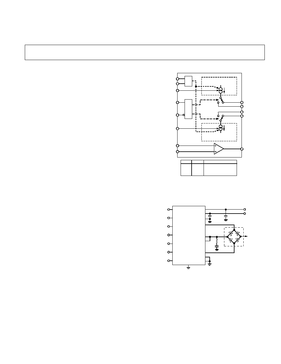
FUNCTIONAL BLOCK DIAGRAM
FEATURES
50 mA Voltage Programmable Current Range
Three Selectable Gain Ranges
1.7 ns Propagation Delay
Inhibit Mode Function
High Speed Differential Inputs for Maximum Flexibility
Ultrasmall 20-Lead PSOP Package with Built-In Heatsink
APPLICATIONS
Automatic Test Equipment
Semiconductor Test Systems
Board Test Systems
PRODUCT DESCRIPTION
The AD53041 is a complete, high speed, current switching load
designed for use in linear, digital or mixed signal test systems.
Combining a high speed monolithic process with a unique sur-
face mount package, this product attains superb electrical per-
formance while preserving optimum packaging densities in an
ultrasmall 20-lead, PSOP package with a built-in heatsink.
Featuring current programmability of up to
±
50 mA, the
AD53041 is designed to force the device under test to source
or sink the programmed I
OH
and I
OL
currents. I
OH
and I
OL
currents are determined by applying a corresponding voltage
(5 V = 50 mA, 16 mA, 5 mA) to the I
OHPGM
and I
OLPGM
pins.
The voltage-to-current conversion is performed within the
AD53041, thus allowing the current levels to be set by a stan-
dard voltage out digital-to-analog converter.
The AD53041 transition from I
OH
to I
OL
occurs when the out-
put voltage of the device under test slews above or below the
programmed threshold or commutation voltage. The commuta-
tion voltage is programmable from 2 V to +7 V, covering the
large spectrum of logic devices while able to support the large
current specifications (48 mA) typically associated with line
drivers. To test I/O devices, the active load can be switched into
a high impedance state (Inhibit Mode), electrically removing the
active load from the path through the Inhibit Mode feature. The
active load leakage current in Inhibit is typically 100 nA.
The Inhibit input circuitry is implemented using high speed
differential inputs with a common-mode voltage range of
2 V to +3 V and a maximum differential voltage of 3 V. This
allows for direct interface to precision differential ECL timing or
the simplicity of switching active load from a single ended TTL
or CMOS logic source. With switching speeds from I
OH
or I
OL
into Inhibit of less than 2.0 ns, the AD53041 can be electrically
removed from the signal path "on the fly."
The AD53041 is available in a 20-lead, PSOP package with a
built-in-heatsink and is specified to operate over the ambient
commercial temperature range from 25
°
C to +85
°
C.
V
CC
V
EE
AGND
I
OLOUT
V
COMOUT
I
OHOUT
OUT_SENSE
I
OLRTN
I
OHRTN
INH
INH
I
OHPGM
V
COMIN
I
OLPGM
GAINA
GAINB
GND
AD53041
TO DUT
0.1 F
0.1 F
1
0.1 F
HSMS-2818
OR EQUIV.
NOT SHOWN: THE AGND PINS ARE THE HIGH QUALITY GROUND
REFERENCE FOR THE VOLTAGE-TO-CURRENT CONVERTERS.
THE GND PINS PROVIDE RETURN PATHS FOR INTERNAL CURRENTS.
V
CC
IS THE POSITIVE SUPPLY, V
EE
IS THE NEGATIVE SUPPLY.
ALL GROUND PINS SHOULD BE CONNECTED TO THE SYSTEM
ANALOG GROUND PLANE.
Figure 1. Typical Application Circuit
VOLTAGE-TO-CURRENT
CONVERTER
VOLTAGE-TO-CURRENT
CONVERTER
AD53041
I
OLOUT
I
OLRTN
I
OHRTN
I
OHOUT
V
COMOUT
V
COM
BUFFER
INH
INH
I
OHPGM
V
COMIN
OUT_SENSE
I
OLPGM
GAINB
GAINA
GAINA GAINB FULL-SCALE CURRENT
0
0
1
1
0
1
0
1
50mA
16mA
5mA
NOT VALID

2
REV. A
AD53041SPECIFICATIONS
(All specifications apply at T
J
= +85 C 5 C. +V
S
= +10.5 V 3%, V
S
=
5.2 V 3% unless otherwise specified. V
COMOUT
is bypassed to ground with a series RC consisting of a 1
resistor and a 0.1 F capacitor,
and is also connected directly to OUT_SENSE. All temperature coefficients are characterized over T
J
= 75 C95 C.)
Parameter
Min
Typ
Max
Units
Test Conditions
INPUT CHARACTERISTICS
INH,
INH
Input Voltage
2
ECL
0
V
Bias Current
1
1
mA
INH,
INH = 2 V, 0 V
GAINA, GAINB
Input Voltage
0
TTL/CMOS
5
V
Bias Current
0
2
mA
GAINA, GAINB = 5 V
I
OHPGM
, I
OLPGM
Voltage Range
I
OH
, 0 to + Full Scale, Any Gain Range
0.1
5.2
V
V(I
OHOUT
) = 2 V, 7 V
I
OL
, 0 to Full Scale, Any Gain Range
0.1
5.2
V
V(I
OLOUT
) = 2 V, 7 V
I
OHPGM
, I
OLPGM
Bias Current
300
300
µ
A
V(I
OHPGM
) = +5 V, V(I
OLPGM
) = 0 V
V
COM
BUFFER
Voltage Range
2
7
V
±
50 mA Output Current
Offset
±
5
mV
V
COM
= 0 V
Offset Drift
0.1
mV/
°
C
V
COM
= 0 V
Nonlinearity
±
5
mV
V
COM
= 2 V to 7 V
Input Bias Current
50
50
µ
A
V
COM
= 2 V to 7 V
Output Resistance
<1
V
COM
= 0 V, I
OUT
=
±
50 mA
OUTPUT CHARACTERISTICS
Full-Scale Current Range
See Functional Block Diagram
Range 0
50
mA
Range 1
16
mA
Range 2
5
mA
Offset Error
V(I
OHPGM
) = V(I
OLPGM
) = 100 mV,
Range 0
1
1
mA
V(I
OHOUT
) =
±
2 V, V(I
OLOUT
) =
±
2 V
Range 1
0.3
0.3
mA
Range 2
0.3
0.3
mA
Offset Drift
V(I
OHPGM
) = V(I
OLPGM
) = 100 mV,
Range 0
1
µ
A/
°
C
V(I
OHOUT
) = V(I
OLOUT
) = 0 V
Range 1
1
µ
A/
°
C
Range 2
1
µ
A/
°
C
Gain Error
Range 0
<1
% FSR
Range 1
<5
% FSR
Range 2
<8
% FSR
Gain Drift
Range 0
1
µ
A/
°
C
Range 1
0.5
µ
A/
°
C
Range 2
0.3
µ
A/
°
C
Gain Ratio Drift
Range 1 to Range 0
0.01
%/
°
C
Range 2 to Range 0
0.01
%/
°
C
Nonlinearity
±
0.05
% FSR
Range 0
Common-Mode Error
±
0.05
%FSR
Range 0
PSRR
±
0.1
%FSR/V
Range 0, V(I
OHPGM
) = V(I
OLPGM
)
= 100 mV, Either Supply Over Operating
Range
OUTPUT VOLTAGE RANGE
I
OHOUT
, I
OHRTN
2.5
7.5
V
I
OH
= 50 mA
I
OLOUT
, I
OLRTN
2.5
7.5
V
I
OL
= 50 mA
3
REV. A
AD53041
Parameter
Min
Typ
Max
Units
Test Conditions
LEAKAGE CURRENTS
Range 0, Bridge Diode Leakage Not Included
I
OH
Inhibit-Mode Leakage
1
1
µ
A
V(I
OHOUT
) = 2.5 V to 7.5 V, Inhibited
I
OL
Inhibit-Mode Leakage
1
1
µ
A
V(I
OLOUT
) = 2.5 V to 7.5 V, Inhibited
I
OH
Off-State Leakage
3
3
µ
A
V(I
OHOUT
) = 2.5 V to 7.5 V, V(I
OHPGM
)
= 0.2 V
I
OL
Off-State Leakage
3
3
µ
A
V(I
OLOUT
) = 2.5 V to 7.5 V, V(I
OLPGM
)
= 0.2 V
DYNAMIC PERFORMANCE
Propagation Delays
±
I
MAX
to Inhibit
1.4
ns
Range 0, I
MAX
, R
LOAD
= 50
Part-to-Part Skew
1
ns
Inhibit to
±
I
MAX
1.9
ns
Range 0, I
MAX
, R
LOAD
= 50
Part-to-Part Skew
1
ns
Propagation Delay Drift
10
ps/
°
C
±
I
MAX
to Inhibit, Inhibit to
±
I
MAX
Capacitance
3
pF
I
OHOUT
or I
OLOUT
Without Diodes
POWER SUPPLIES
V
S
to +V
S
Range
15.2
15.7
16.2
V
Positive Supply Range
10.2
10.5
10.8
V
Negative Supply Range
5.4
5.2
5.0
V
Positive Supply Current
160
mA
Range 0, V(I
OHPGM
) =
V(I
OLPGM
) = 5.0 V, Active
10
60
mA
Range 0, V(I
OHPGM
) =
V(I
OLPGM
) = 200 mV, Active
Negative Supply Current
160
mA
Range 0, V(I
OHPGM
) =
V(I
OLPGM
) = 5.0 V, Active
10
60
mA
Range 0, V(I
OHPGM
) =
V(I
OLPGM
) = 200 mV, Active
Power Dissipation
2.1
2.3
W
I
OH
= 50 mA, I
OL
= 50 mA, Active,
V(I
OHOUT
) = 7 V, V(I
OLOUT
) = 2 V
NOTES
Typical values are not tested or guaranteed.
Specifications subject to change without notice.
Table I. Active Load Truth Table
(Including External Diode Bridge per Figure 1; Scale Factors per Functional Block Diagram)
OUTPUT STATES (IFS Is Full-Scale Current Set by GAINA, GAINB)
V(DUT)
INH
INH
I
OH
I
OL
I(VDUT)
< V
COM
0
1
[V(I
OHPGM
)
÷
5 V]
×
IFS
[V(I
OLPGM
)
÷
5 V]
×
IFS
I
OL
> V
COM
0
1
[V(I
OHPGM
)
÷
5 V]
×
IFS
[V(I
OLPGM
)
÷
5 V]
×
IFS
I
OH
X
1
0
0
0
0
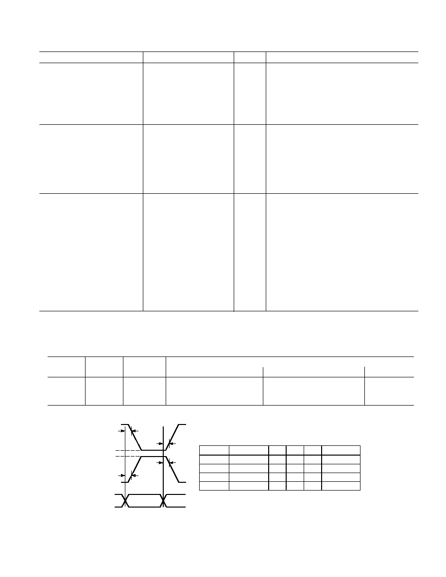
Figure 2. Inhibit Propagation Delay Measurement
t
pdIH
t
pdIL
t
pdAH
t
pdAL
Vact
Vact+
V
DUT
V
DUT
ECL+
ECL
PARAMETER
t
pdAH
t
pdIL
t
pdAH
t
pdIH
DESCRIPTION
I
OL
Inh
Act
I
OL
Act
Inh
I
OH
Inh
Act
I
OH
Act
Inh
I
OL
50mA
50mA
50mA
50mA
I
OH
50mA
50mA
50mA
50mA
V
DUT
0V
0V
5V
5V
MEASURE POINT
0.50V
2.00V
4.50V
3.00V
PROPAGATION DELAY LOAD AND TEST CONDITIONS
AD53041
4
REV. A
C3004a011/98
PRINTED IN U.S.A.
CAUTION
ESD (electrostatic discharge) sensitive device. Electrostatic charges as high as 4000 V readily
accumulate on the human body and test equipment and can discharge without detection.
Although the AD53041 features proprietary ESD protection circuitry, permanent damage may
occur on devices subjected to high energy electrostatic discharges. Therefore, proper ESD
precautions are recommended to avoid performance degradation or loss of functionality.
ABSOLUTE MAXIMUM RATINGS
1
Power Supply Voltage
+V
S
to GND . . . . . . . . . . . . . . . . . . . . . . . . . . . . . . . +12 V
V
S
to GND . . . . . . . . . . . . . . . . . . . . . . . . . . . . . . . . . 7 V
+V
S
to V
S
. . . . . . . . . . . . . . . . . . . . . . . . . . . . . . . . . +17 V
GND to AGND . . . . . . . . . . . . . . . . . . . . . . . . . . . .
±
0.4 V
Inputs
INH,
INH . . . . . . . . . . . . . . . . . . . . . . . . . . . . . +6 V, 3 V
INH to
INH . . . . . . . . . . . . . . . . . . . . . . . . . . . . . . . .
±
3 V
GAINA, GAINB . . . . . . . . . . . . . . . . . . . . . . . . +6 V, 3 V
GAINA to GAINB . . . . . . . . . . . . . . . . . . . . . . . . . . . .
±
5 V
V
COMIN
. . . . . . . . . . . . . . . . . . . . . . . . . . . . . . . +8 V, 3 V
I
OHPGM
, I
OLPGM
. . . . . . . . . . . . . . . . . . . . . . . . . +6 V, 1 V
Outputs
I
OHOUT
, I
OHRTN
. . . . . . . . . . . . . . . . . . . . . . . . +9 V, 2.5 V
I
OLOUT
, I
OLRTN
. . . . . . . . . . . . . . . . . . . . . . . . . +8 V, 3.5 V
V
COMOUT
Short Circuit Duration . . . . . . . . . Not Protected
2
Environmental
Operating Temperature (Junction) . . . . . . . . . . . . . . +175
°
C
Storage Temperature . . . . . . . . . . . . . . . . 65
°
C to +150
°
C
Lead Temperature (Soldering, 10 sec)
3
. . . . . . . . . . +260
°
C
NOTES
1
Stresses above those listed under Absolute Maximum Ratings may cause per ma-
nent damage to the device. This is a stress rating only; functional operation of the
device at these or any other conditions above those indicated in the operational
sections of this specification is not implied. Absolute maximum limits apply
individually, not in combination. Exposure to absolute maximum rating condi-
tions for extended periods may affect device reliability.
2
Short circuit to ground or to either supply will result in the destruction of the
device.
3
To ensure lead coplanarity (
±
0.002 inches) and solderability, handling with bare
hands should be avoided and the device should be stored in environments at 24
°
C
±
5
°
C (75
°
F
±
10
°
F) with relative humidity not to exceed 65%.
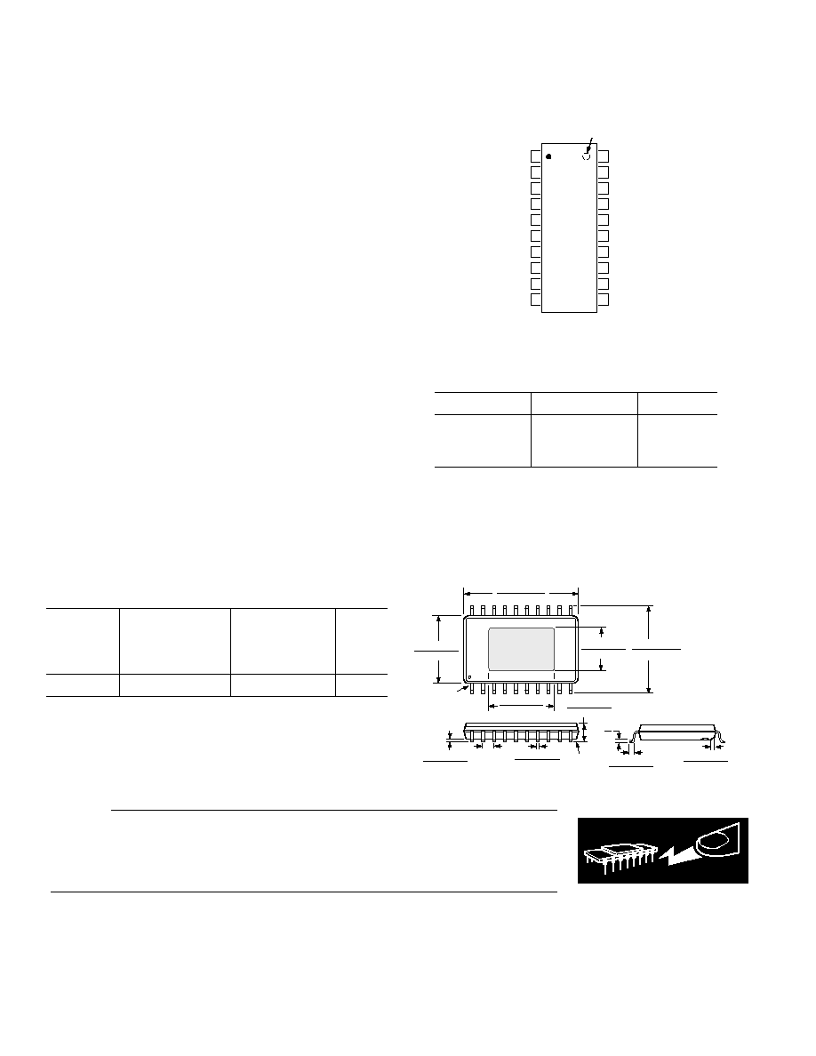
PIN CONFIGURATION
PACKAGE THERMAL CHARACTERISTICS
Air Flow, FM
JC
, C/W
JA
, C/W
0
4
50
50
4
49
400
4
34
OUTLINE DIMENSIONS
Dimensions shown in inches and (mm).
20-Lead Thermally Enhanced
Power Small Outline Package (PSOP)
(RP-20)
SEATING
PLANE
0.0118 (0.30)
0.0040 (0.10)
0.0201 (0.51)
0.0130 (0.33)
0.1043 (2.65)
0.0926 (2.35)
0.0500
(1.27)
BSC
STANDOFF
0.0500 (1.27)
0.0057 (0.40)
8
°
0
°
0.0295 (0.75)
0.0098 (0.25)
x 45
°
0.5118 (13.00)
0.4961 (12.60)
0.4193 (10.65)
0.3937 (10.00)
0.2992 (7.60)
0.2914 (7.40)
PIN 1
0.3340 (8.61)
0.3287 (8.35)
0.1890 (4.80)
0.1791 (4.55)
20
1
11
10
HEAT
SINK
ORDERING GUIDE
Shipment Method,
Quantity
Package
per Shipping
Package
Model
Description
Container
Option
AD53041KRP 20-Lead Power SOIC Tube, 38 Pieces
RP-20
14
13
12
11
17
16
15
20
19
18
10
9
8
1
2
3
4
7
6
5
TOP VIEW
(Not to Scale)
AGND
V
CC
DGND
GAINA
GAINB
I
OLPGM
I
OLOUT
I
OLRTN
AD53041
V
EE
INH
INH
V
COMIN
V
COMOUT
I
OHRTN
I
OHOUT
DGND
DGND
I
OHPGM
AGND
DGND
DIMPLE ON BOTTOM
OF PACKAGE
NOTES:
AGND IS THE HIGH-QUALITY GROUND REFERENCE
FOR I
OLPGM
AND I
OHPGM
.
DGND IS THE SUPPLY GROUND.
WARNING!
ESD SENSITIVE DEVICE