Äîêóìåíòàöèÿ è îïèñàíèÿ www.docs.chipfind.ru
AD2S93
One Technology Way, P.O. Box 9106, Norwood. MA 02062-9106, U.S.A.
Tel: 617/329-4700
Fax: 617/326-8703
a
Low Cost
LVDT-to-Digital Converter
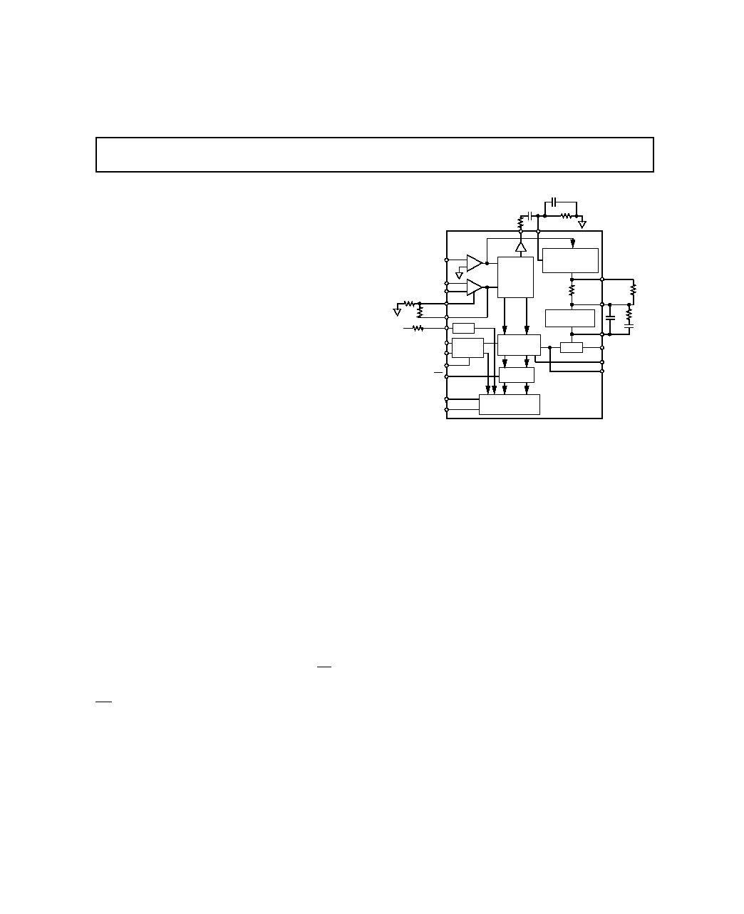
FUNCTIONAL BLOCK DIAGRAM
DEMODIN
CLKOUT
DEMOD OUT
ERROR
AMP
LOS
LATCHES
FREQUENCY
SHAPING
VCO
PHASE
SENSITIVE
DEMODULATOR
C1
C2
R2
VEL
UP-DOWN
COUNTER
REFERENCE
(PRIMARY
EXCITATION)
DIFFERENTIAL
(SECONDARY
VOLTAGE)
REF
A
B
LOS
GAIN
V
DD
OVR
UNR
NULL
CS
DATA
SCLK
ACERROR
AC RATIO
BRIDGE
DIFF
DECODE
LOGIC
C3
AD2S93
INTIN
R4
R3
SERIAL
INTERFACE
DIR
R5
R1
C4
R6
R7
VCO GAIN
FEATURES
Full Function Monolithic LVDT-to-Digital Converter
Absolute Serial Data Output
Uncommitted Differential Input
Repeatability
Remote Diagnostics
14-Bit Resolution
Industrial Temperature Range
28-Pin PLCC
Low Power
APPLICATIONS
Industrial Gauging
Industrial Process Control
Linear Positioning Systems
Linear Actuator Control
Automotive Motion Sensing and Control
Torque Sensing Conditioner
AC Strain Gages Conditioning
Avionics
REV. A
Information furnished by Analog Devices is believed to be accurate and
reliable. However, no responsibility is assumed by Analog Devices for its
use, nor for any infringements of patents or other rights of third parties
which may result from its use. No license is granted by implication or
otherwise under any patent or patent rights of Analog Devices.
GENERAL DESCRIPTION
The AD2S93 is a complete 14-bit resolution tracking LVDT-to-
digital converter. A Type II tracking loop is employed to track
the AB input and produce a digital output equal to (AB)/
(REF/2), where REF is a fixed amplitude ac reference phase co-
herent with the AB input. This allows the measurement of any
2-, 3-, 4- and 5-wire LVDT or linear amplitude modulated in-
put. The operating frequency range is from 360 Hz to 10 kHz
with user definable bandwidth set externally within a range of
45 Hz to 1250 Hz.
The AD2S93 has a 16-bit serial output. The MSB (LOS), read
first, indicates a loss of the signal A, B, or reference inputs to the
converter or transducer. The second and third MSBs are flags
indicating whether [REF/2 (UNR)
AB
+REF/2 (OVR]) is
outside the linear operating range of the converter. The dis-
placement data is presented as 13-bit offset binary giving a
±
12-
bit operating range. LOS, OVR and UNR are pinned out on
the device, in addition a NULL flag is available which is set
when (AB) = 0.
Absolute displacement information is accessed when CS is taken
LO followed by the application of an external clock (SCLK)
with a maximum rate of 2 MHz. Data is read MSB first. When
CS
is high the DATA output is high impedance; this allows
daisy chaining of more than one converter onto a common bus.
The A, B differential input allows the user to scale the A, B in-
puts between 1 and 10. This enables the user to accurately set
up the inputs matching the REF input to the DIFF output. The
DIFF output is the resultant AB. The AD2S93 operates using
±
5 V
±
5% power supplies and is fabricated on Analog Devices'
linear compatible CMOS process (LC
2
MOS). The (LC
2
MOS)
is a mixed technology process that combines precision bipolar
circuits with low power logic.
PRODUCT HIGHLIGHTS
Complete LVDT-to-Digital Interface.
The AD2S93 pro-
vides the complete solution for digitizing LVDT signals to 14-
bit resolution.
Serial 16-Bit Output Data.
One 16-bit read from the
AD2S93 determines input signal continuity (LOS), over and
underrange detection and 13 bits of offset binary displacement
information.
High Accuracy Grade in Low Cost Package.
0.05% and
0.1% integral linearity over the full 40
°
C to +85
°
C operating
temperature range.
Uncommitted Differential Input.
Allows configuration of 2-,
3-, 4- and 5-wire LVDTs.
Multiple Converter Interfacing.
High impedance data out-
put and a simple three-wire interface reduces cabling and elimi-
nates bus contention.
Low
Power. 70 mW power consumption (typ).

Parameter
Test Conditions
Min
Typ
Max
Units
SIGNAL INPUTS
Frequency
0.36
1.0
10
kHz
Max Voltage Level
1
0.8
1.0
1.2
V rms
Nominal Full Scale
2
1.0
V rms
Input Bias Current
@ +25
°
C
1.1
µ
A
Input Impedance
1.0
M
CMRR
57
dB
Maximum Sensitivity
3
V
AB
= 1 V rms, G = 1
342
µ
V pk/LSB
REFERENCE INPUT
Frequency
0.36
10
kHz
Voltage Level
1.8
2.0
2.2
V rms
Input Bias Current
@ 0 V +25
°
C
1
µ
A
Input Impedance
1.0
M
Permissible Phase Shift
4
Signal to Reference
10
+10
Degrees
CONVERTER DYNAMICS
Bandwidth
Set by User
VCO Mode = 1
VCO Gain Connected to
VCO I/P
500
1250
Hz
VCO Mode = 2
VCO Gain No Connect
45
500
Hz
Maximum Slew Rate
Mode = 1
2400
3000
LSB/ms
Mode = 2
800
1000
LSB/ms
ACCURACY
Integral Linearity
AP
0.1
% FSD
BP
0.05
% FSD
Differential Linearity
AP
<2
LSB
BP
<1
LSB
Repeatability
±
1
LSB
Zero Position Offset
AP @ +25
°
C
3
3
LSB
BP @ +25
°
C
1
1
LSB
AP @ 40
°
C to +85
°
C
4
4
LSB
BP @ 40
°
C to +85
°
C
2
2
LSB
Gain Error
±
0.7
% FS
VELOCITY OUTPUT
Max Output Voltage
Denotes Max Input Speed
±
4.0
V dc
Load Drive Capability
±
250
µ
A
LOGIC INPUTS SCLK, CS
Input High Voltage V
INH
3.5
V dc
Input Low Voltage V
INL
1.5
V dc
Input Current I
IN
500
nA
Input Capacitance
10
pF
LOGIC OUTPUTS
OVR, UNR, NULL, DATA, A, B CLKOUT DIR
Output High Voltage
@ 1 mA
4.0
V dc
Output Low Voltage
@ 1 mA
1.0
V dc
LOS OUTPUT
Open Drain Output
Pull-Up to +V
DD
via 12 k
400
µ
A
Drive Capability
Signal Threshold (A-B)
0.1
0.2
V rms
REF Threshold
0.22
V rms
Timeout Threshold
50
ms
AD2S93SPECIFICATIONS
REV. A
2
(V
DD
= +5 V
±
5%; V
SS
= 5 V
±
5%, AGND = DGND = 0 V, T
A
=
40
°
C to +85
°
C
unless otherwise noted)
AD2S93
REV. A
3
Parameter
Test Conditions
Min
Typ
Max
Units
SERIAL CLOCK (SCLK)
SCK Input Rate
2
MHz
Maximum Read Rate (16 Bits)
Continuous
9.2
µ
s
POWER SUPPLY
I
DD
5
7
10
mA
I
SS
5
7
10
mA
NOTES
1
The signal input voltage maximum should always be set at 10% less than the reference input.
2
Nominal + FS = V
AB
= V
REF
/2, FS = V
AB
= V
REF
/2
3
With G = 10; Sensitivity 34.2
µ
V pk/LSB
4
Phase shift cause gain errors. "See Phase Shift and Quadrative Effects."
Specifications subject to change without notice.
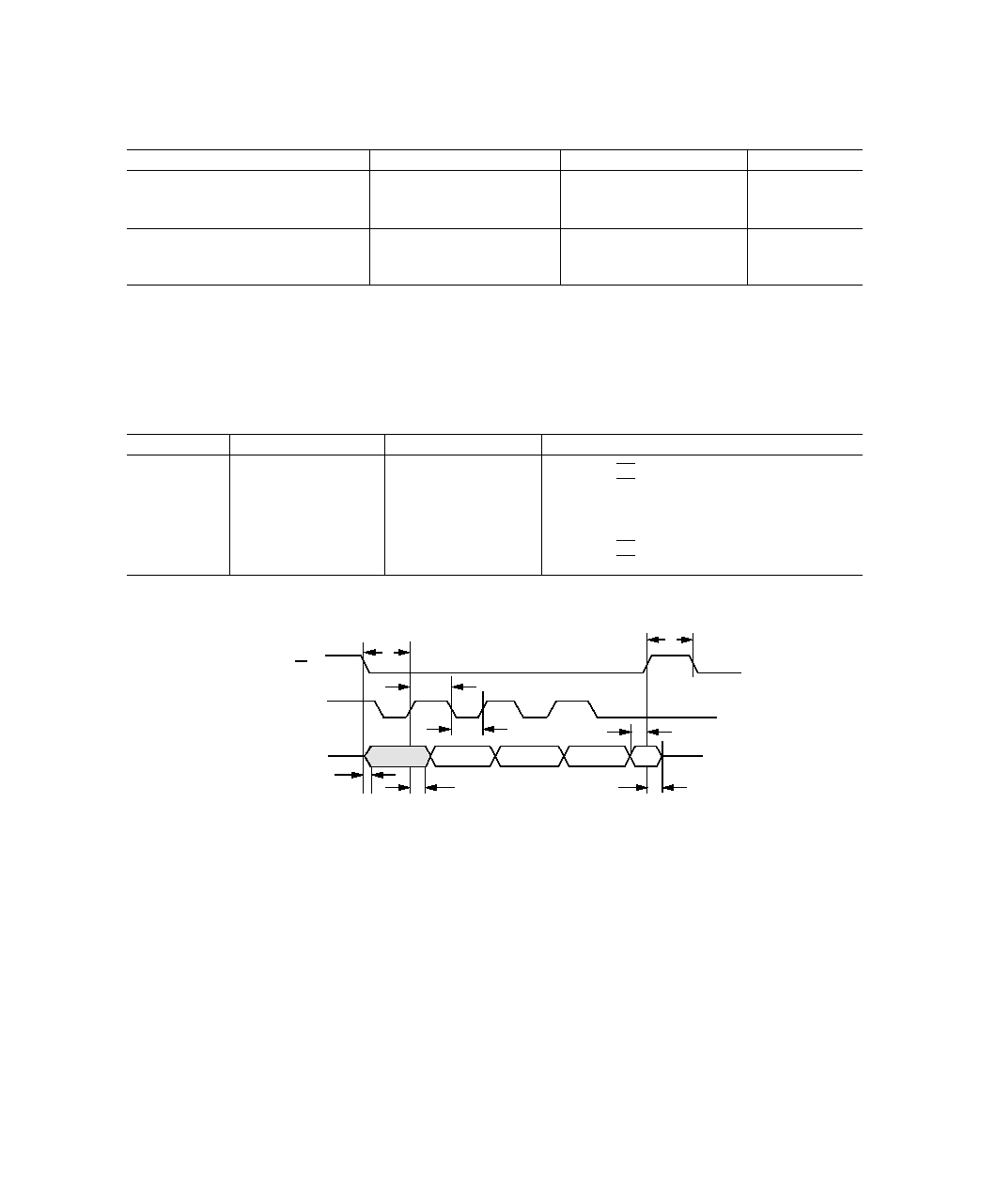
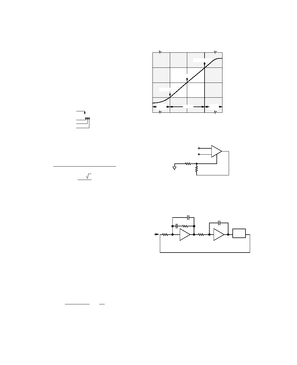
SCLK
DATA
CS
t
*
t
3
t
4
t
1
t
5
t
7
LSB
MSB
t * = THE MINIMUM ACCESS TIME: USER DEPENDENT
TOTAL MAX READ TIME =
t
2
+ 16. (
t
3
+
t
4
) +
t
7
TOTAL MAX READ TIME = 600 +16 (250 + 250) + 150 ns
TOTAL MAX READ TIME = 600 + 8000 + 150 ns
TOTAL MAX READ TIME = 8.750 µs (SINGLE READ ONLY)
t
2
t
6
Timing Diagram
Parameter
AD2S93
Units
Test Conditions
t
1
1
150
ns max
CS
to DATA Enable
t
2
600
ns min
CS
to 1st SCLK Positive Edge
t
3
250
ns min
SCLK High Pulse
t
4
250
ns min
SCLK Low Pulse
t
5
100
ns max
SCLK Positive Edge to DATA Valid
t
6
600
ns min
CS
High Pulse Width
t
7
150
ns max
CS
High to DATA High Z (Bus Relinquish)
NOTE
1
SCLK can only be applied after t
2
has elapsed.
TIMING CHARACTERISTICS
(V
DD
= +5 V
±
5%, AGND = DGND = 0 V, T
A
= 40
°
C to +85
°
C unless otherwise noted)
4
REV. A
AD2S93
ORDERING GUIDE
Temperature
Package
Model
Range
Linearity
Option
AD2S93AP
40
°
C to +85
°
C
0.1%
P-28A
AD2S93BP
40
°
C to +85
°
C
0.05%
P-28A
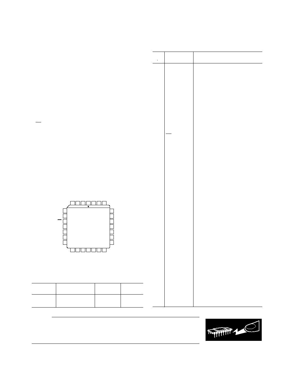
PIN DESIGNATIONS
Pin
No.
Mnemonic
Description
1
AGND
Analog Ground.
2
DIFF
Output of Signal Input Preamplifier.
3
GAIN
Connect GAIN Pin to DIFF for
nominal
×
1. Gains greater than
1 can be resistively scaled.
Do not leave unconnected.
4
LOS
Denotes A or B lines loss of
connection and/or loss of reference
to transducer or converter.
5
DATA
16-bit serial data output 13 bits of
absolute position information plus
overrange and underrange plus LOS.
6
SCLK
Serial Clock. Maximum rate = 2 MHz.
7
CS
Chip Select. Loads serial interface
with current positional information
and enable output.
9, 12
UNR, OVR
Two pins that denote whether the
input signals are underrange or
overrange.
10
CLKOUT
Updates every LSB.
13
NULL
Denotes Null Position.
14
DIR
Indicates direction. DIR is HI for
positive displacement and LO for
negative displacement.
15
DGND
Digital Ground.
16
V
SS
Negative Power Supply 5.0 V dc
±
5%.
17
V
DD
Positive Power Supply +5.0 V dc
±
5%.
18
DEMODOUT Output of the Phase Sensitive
Demodulator.
19
DEMODIN
Input to Phase Sensitive
Demodulator.
20
ACERROR
AC Error Output.
21
VCO GAIN
Sets the VCO gain internally.
Connect to VEL for 2400 LSB/s.
Disconnect for 800 LSB/s.
22
INTIN
Determines system dynamics connect
C and RC (serial) parallel
combination across INTIN and
VEL to determine loop dynamics.
23
VEL
Analog Velocity Output.
24
REF
Single ended input for fixed
amplitude reference.
27, 28 B, A
Uncommitted differential inputs
for the A, B signal inputs.
CAUTION
ESD (electrostatic discharge) sensitive device. Electrostatic charges as high as 4000 V readily
accumulate on the human body and test equipment and can discharge without detection.
Although the AD2S93 features proprietary ESD protection circuitry, permanent damage may
occur on devices subjected to high energy electrostatic discharges. Therefore, proper ESD
precautions are recommended to avoid performance degradation or loss of functionality.
WARNING!
ESD SENSITIVE DEVICE
RECOMMENDED OPERATING CONDITIONS
Power Supply Voltage (V
DD
V
SS
) . . . . . . . . . . .
±
5 V dc
±
5%
Analog Input Voltage (A, B) . . . . . . . . . . . . . . 1 V rms
±
10%
Analog Reference Input (REF) . . . . . . . . . . . . 2 V rms
±
10%
Signal and Reference Harmonic Distortion . . . . . . . . . . . <10%
Operating Temperature Range
Industrial (AP, BP) . . . . . . . . . . . . . . . . . . . 40
°
C to +85
°
C
ABSOLUTE MAXIMUM RATINGS*
V
DD
to AGND . . . . . . . . . . . . . . . . . . . 0.3 V dc to + 7.0 V dc
V
SS
to AGND . . . . . . . . . . . . . . . . . . . +0.3 V dc to 7.0 V dc
AGND to DGND . . . . . . . . . . . . 0.3 V dc to V
DD
+ 0.3 V dc
Analog Inputs to AGND REF . . . . V
SS
0.3 V to V
DD
+ 0.3 V
A, B . . . . . . . . . . . . . . . . . . . . . . . . . V
SS
0.3 V to V
DD
+ 0.3 V
Analog Output to AGND VEL . . . . . . . . . . . . . . . . V
SS
to V
DD
Digital Inputs to DGND
CS
, SCLK . . . . . . . . . . . . . . . . . . . . . 0.3 V to V
DD
+ 0.3 V
Digital Outputs to DGND
NULL, DIR, CLKOUT, DATA . . . . 0.3 V to V
DD
+ 0.3 V
Operating Temperature Range
Industrial (A, B) . . . . . . . . . . . . . . . . . . . . . 40
°
C to +85
°
C
Lead Temperature (Soldering 10 sec) . . . . . . . . . . . . . +300
°
C
Power Dissipation to +75
°
C . . . . . . . . . . . . . . . . . . +100 mW
Derates above +75
°
C by . . . . . . . . . . . . . . . . . . . . . 10 mW/
°
C
*
Stresses above those listed under "Absolute Maximum Ratings" may cause
permanent damage to the device. This is a stress rating only and functional
operation of the device at these or any other conditions above those indicated in the
operational section of this specification is not implied. Exposure to absolute
maximum rating conditions for extended periods may affect device reliability.
NC = NO CONNECT
NC
REF
VCOGAIN
ACERROR
DEMODIN
VEL
INTIN
DATA
SCLK
UNR
CLKOUT
NC
CS
NC
LOS
GAIN
A
B
NC
DIFF
OVR
NULL
V
SS
V
DD
DEMODOUT
DIR
DGND
AGND
26
27
28
4
2
3
15
18
17
16
12
14
13
25
24
21
20
19
23
22
TOP VIEW
(Not to Scale)
1
5
6
9
10
11
7
8
AD2S93
5
REV. A
AD2S93
GLOSSARY OF TERMS
INTEGRAL LINEARITY
Integral linearity deviation as a percent of full scale. A 0.1% de-
viation is equivalent to 8-LSB change on the output.
Gain
The converter gain is the maximum variation in the ratio of
AB/REF/2 to the maximum digital input.
Output Offset
The output offset is the digital output code when the analog in-
put signal AB = 0.
Overrange (OVR)
OVR goes high when AB is in phase with REF and larger than
REF/2.
Underrange (UNR)
UNR goes high when AB is out of phase with REF and larger
than REF/2.
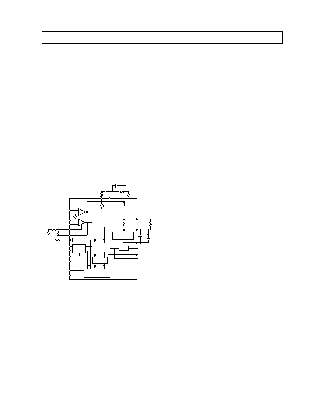
PRINCIPLE OF OPERATION
The AD2S93 is based on a Type 2 tracking closed-loop prin-
ciple. The output tracks the position of the LVDT without the
need for external convert and wait states. As the transducer
moves through a position equivalent to the least significant bit
weighting, the output is updated by one LSB. On the AD2S93,
CLKOUT updates corresponding to one LSB increment. Fig-
ure 1 illustrates the principle of operation.
DEMODIN
CLKOUT
DEMOD OUT
ERROR
AMP
LOS
LATCHES
FREQUENCY
SHAPING
VCO
PHASE
SENSITIVE
DEMODULATOR
C1
C2
R2
VEL
UP-DOWN
COUNTER
REFERENCE
(PRIMARY
EXCITATION)
DIFFERENTIAL
(SECONDARY
VOLTAGE)
REF
A
B
LOS
GAIN
V
DD
OVR
UNR
NULL
CS
DATA
SCLK
ACERROR
AC RATIO
BRIDGE
DIFF
DECODE
LOGIC
C3
AD2S93
INTIN
R4
R3
SERIAL
INTERFACE
DIR
R5
R1
C4
R6
R7
VCO GAIN
Figure 1. Functional Block Diagram
Because the conversion depends on the ratio of the input signals
(ratiometric ac bridge), the AD2S93 is remarkably tolerant of
input amplitude and frequency. This, combined with the defin-
able Type 2 tracking closed-loop guarantees the AD2S93's re-
peatability for a given input. A phase sensitive detector,
integrator and voltage controlled oscillator (VCO) form a closed
loop system which seeks to null the output of the ACERROR.
When this is accomplished the word state of the up/down
counter equals within the rated accuracy of the converter, the
LVDT position output.
For more information on the operation of the converter, see
"Circuit Dynamics" section.
DATA FORMAT
OPERATING RANGE
The AD2S93 operating range is defined in Figure 2. The lin-
earity and specified operating range of the converter is the cen-
tral two 12-bit quadrants through zero. The corresponding
input relationship is REF/2
AB
+REF/2, (
±
is used to de-
note phase coherency). The sign bit is low for inputs with AB
in phase with REF. The two remaining 12-bit quadrants are
used to denote over (OVR) and underrange (UNR). OVR goes
high when AB is in phase with REF and larger than REF/2.
UNR goes high when AB is out of phase with REF and larger
than REF/2. LOS is an open drain output which pulls high
when A and/or B are removed or REF is removed (see "Inbuilt
Diagnostics"), or A + B is less than 100 mV.
SCALING THE INPUTS
In order to match the LVDT output to the AD2S93 output, the
inputs to the AD2S93 need to be scaled. The operating range is
illustrated in Figure 2. The AD2S93 operates across
±
12-bit
range where the remaining 12-bit quadrants are used to denote
overrange and underrange. The output position word is a func-
tion of the ratio between AB and V
REF
(see Figure 2) where:
±
FSR
=
( A
-
B )
V
REF
/2
6
REV. A
AD2S93
+VE POSITION
FULL SCALE
VE POSITION
FULL SCALE
NULL
POSITION
OUTPUT CODES
MAGNITUDE
0100
0000
0000
0000
0100
1111
1111
1111
0100
0000
0000
0000
0000
0000
0000
0001
0000
1111
1111
1111
0001
0000
0000
0000
0001
0000
0000
0001
0001
1111
1111
1110
0001
1111
1111
1111
0011
0000
0000
0000
0011
0000
0000
0001
0011
1111
1111
1111
RANGE
OVER-
RANGE
1
0
1
RATIO OF A- B/REF/2
A B = REF/2
A B = + REF/2
A B = 0
UNDER-
RANGE
LOS
OVR
UNR
SIGN
Figure 2. Output Code Format
If the maximum operating stroke of an LVDT yielded a 1 V rms
AB output, the weighting of the LVDT to AD2S93 digital out-
put would be:
Input Signal Full Scale
Full-Scale Operating Range (
±
2
12
)
1
×
2 2
2
13
Input Scaling
=
345
µ
V/LSB
This can be equated directly to the LVDT sensitivity specifica-
tion in mm/v/v.
Note: The overrange and underrange quadrants can be utilized
by decoding the overrange and underrange MSBs and decoding
the 12 magnitude bits. This will increase the operating range of
the AD2S93 accordingly. However, if the input AB > V
REF
then the converter will lose track of the input and will only re-
gain track when the input signal returns to within the operating
range of the converter.
INPUT GAIN
Since the transformation ratio of an LVDT or RVDT from exci-
tation voltage to signal voltage can be 1:0.15, provision for gain
scaling has been provided. The gain can, therefore, be selected
to ensure that the full-scale output of converter represents the
maximum stroke position of the transducer.
The gain setting is accomplished by connecting Pin 2, (DIFF)
and Pin 3 (GAIN) together (unity gain) or connecting two resis-
tors as shown in Figure 3.
The gain of the input stage is calculated using the following
equation:
DIFF ( A B)
( A B) IN
=
1
+
R
3
R
4
e.g., For a gain of 5, R3 = 12 k
, R4 = 3 k
For a gain of 10, R3 = 18 k
, R4 = 2 k
AGND
R4
R3
GAIN
DIFF
A
B
Figure 3. Pre-Amp Gain Block
SETTING THE CONVERTER BANDWIDTH
The AD2S93 bandwidth is set by placing three external compo-
nents, C1, C2, and R2, around the integrator as illustrated by
the figure below.
TH
I
R1
C2
C1
R2
C
V
R
V
TH
O
62.5
VCO
INT
Figure 4. Integrator and VCO
Before the bandwidth can be set, the corresponding VCO gain
setting must be determined. The VCO gain is directly related to
the slew rate of the converter. This is set internally to two dif-
ferent rates defined internally by R
V
.
Typical converter slew rates are defined below,
G (1) = 2400 LSB/msMode 1
G (2) = 800 LSB/msMode 2

7
REV. A
AD2S93
Calculation of the component values for the bandwidth is de-
tailed below. For more detailed information on component
value selection for the AD2S93, please consult the "Passive
Component Selection and Dynamic Modeling Software for the
AD2S93 LVDT-to-Digital Converter."
VCO Gain G (1) Mode 1
The available bandwidth with this option is from 0.5 kHz to
1.25 kHz.
F
REF
> 8
×
Fo
C1 = 1/(800
×
Fo
2
)
C2 = 8
×
C1
R2 = 45
×
Fo
Where F
REF
is the reference frequency, Fo is the closed-loop
3 dB point.
VCO Gain G (2) Mode 2
The available bandwidth with this option is from 45 Hz
to 500 Hz.
F
REF
> 8
×
Fo
C1 = 1/(2400
×
Fo
2
)
C2 = 8 C1
R2 = 45
×
Fo
Where F
REF
is the reference frequency, Fo is the closed-loop
3 dB point.
INTERFACING TO THE AD2S93 (SEE "TIMING
CHARACTERISTICS")
The absolute position information is extracted via a three-wire
interface, DATA, CS and SCLK. The DATA output is held in
a high impedance state when CS is high.
Upon the application of logic low to the CS pin, the DATA is
enabled and the current position information is transferred from
the counters to the serial interface. Data is retrieved by applying
an external clock to the SCLK pin. The maximum data rate of
the SCLK is 2 MHz. To ensure secure data retrieval, it is
important to note that SCLK should not be applied until a
minimum period of 600 ns after the application of logic low to
CS
. Data is then clocked out on successive positive edges of
SCLK: 16 clock edges are required to extract the entire data
word. Subsequent positive edges greater than the defined reso-
lution of the converter will clock zeros from the data output if
CS
remains in a low state. The format of the data read is shown
in Table I.
Table I.
DB0
DB1
DB2
DB3
DATA DB4D15
MSB LSB
Function
LOS
OVR
UNR
SIGN
MAGNITUDE
If less than the full 16-bit word is required, then the data read
can be terminated by releasing CS after the required number of
bits have been read.
CS
can be released a minimum of 100 ns after the last positive
edge. If the user is reading data continuously, CS can be reap-
plied after a minimum of 600 ns after it is released. The mini-
mum repetitive read time of the same converter is given by (16
bits read @ 2 MHz). Min RD Time = [600 + (16
×
500) +
600] = 9.2
µ
s.
IN-BUILT DIAGNOSTICS
The first three bits read from the serial interface preceding the
sign and magnitude data can be used to determine whether the
data is valid or not. Over and underrange (OVR, UNR) denote
the two extremes of the LVDT stroke where linearity of the
LVDT may degrade. Loss of signal LOS is an open drain out-
put which pulls high (12 k
pull up) when one of the following
conditions is satisfied:
1. A and/or B is disconnected.
2. REF is disconnected.
Note: LOS has a response time of 50 ms max to the conditions
stated above, see "Specifications."
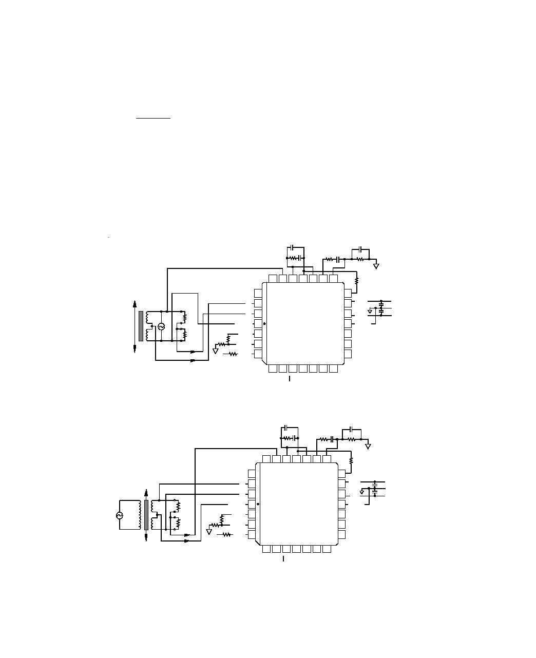
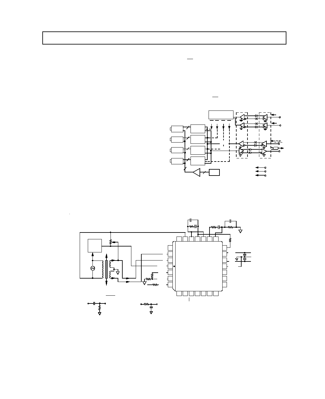
CONNECTING THE CONVERTER
Positive power supply V
DD
= +5 V dc
±
5% should be con-
nected to Pin 17 and negative power supply V
SS
= 5 V dc
±
5%
to Pin 16. Reversal of these power supplies will destroy this device.
For LVDT connections to the converter please refer to Figures
5 through 7. On all connections, the maximum input reference
signal V
REF
= 2.0 V rms
±
10%. To operate within the standard
operating range, AB should not exceed 1.0 V rms
±
10%. The
AD2S93 AGND point is the point at which all analog signal
grounds should be connected. Ground returns from the LVDT
should be connected to AGND. The AD2S93 DGND pin
should be connected to the AD2S93 AGND pin. Ancillary Digi-
tal circuitry must be connected to the Star Point and not to the
AD2S93 AGND pin.
In all cases, the AD2S93 has been configured with the following
dynamics.
Reference Frequency
5 kHz
3 dB Bandwidth
625 Hz
Vco Gain is set in MODE 1 where VCO GAIN is connected to
VEL.
Using the procedure described in "setting the converter band-
width" the following preferred values (E12 series) were calcu-
lated:
C1 = 3.3 nF
C2 = 27 nF
R2 = 27 k
CALCULATING HF FILTER (C3, C4, R5, R6)
15 k
R5 = R6
56 k
C 3 = C4 =
1
2
R5 F
REF
So, C3 = 1 nF, R5 = R6 = 33 k
, C4 = 1 nF and in all cases
R7 = 15 k
.
Half-Bridge Type LVDT Connection
In this method of connection, it is necessary to add two addi-
tional bridge completion resistors R
C
and R
C,
in order to derive
a reference for the AD2S93. In selecting the bridge completion
resistor, it is important to remember that mismatch between R
C1
and R
C2
will cause nonzero errors at null. If two LVDTs are be-
ing used for differential measurements, the resistors can be re-
placed by the second LVDT.
8
REV. A
AD2S93
Three- or Four-Wire LVDT Connection
In this method of connection, shown in Figure 6, the converters
digital output is proportional to the ratio:
( A
-
B )
( A
+
B ) / 2
where A and B are the individual LVDT secondary output volt-
ages. Inspection of Figure 6 should demonstrate why this rela-
tionship is true. (AB) is simply the voltage across the series
connected secondaries of the LVDT and is applied to the A, B
input to the converter. (A + B)/2 is effectively the average of
the two secondary voltages as computed by the balanced bridge
completion resistors and the grounding of the secondary
center-tap.
Note: This method of connection is appropriate only for where
(A + B) is a constant, independent of LVDT position. Any lack
of constancy in (A + B) will be reflected as an additional non-
linearity in the output. It is up to the user to determine if (A +
B) is sufficiently constant over the particular stroke length em-
ployed.
This method will usually restrict the usable LVDT range to half
of its full range. The restriction can be eliminated, however, by
attenuating DIFF by a factor of 2 or increasing V
REF
by a factor
of 2. This connection method has the tremendous advantage of
being insensitive to temperature related phase shifts and excita-
tion oscillator instability effects usually associated with more
conventional LVDT conversion systems.
As in the case of the half-bridge type LVDT connection, R
C1
and R
C2
are the bridge completion resistors and are matched to
a degree sufficient to ensure that the digital output representing
the null position does not vary from the LVDT's natural null
position. If null adjustment is required, a potentiometer can be
used in place of the common connection between the two
resistors.
NC = NO CONNECT
DATA
SCLK
UNR
CLKOUT
NC
NC
NC
OVR
NULL
DEMODOUT
DIR
26
27
28
4
2
3
15
18
17
16
12
14
13
25
24
21
20
19
23
22
1
5
6
9
10
11
7
8
TOP VIEW
(Not to Scale)
AD2S93
CS
+5V
0V
5V
LOS
12k
GAIN
DIFF
AGND
A
B
R4
R3
V
DD
R
C2
R
C1
B
A
R2
C2
C1
C3
R5
REF
PISTON
GND
V
DD
V
SS
DGND
R6
R7
C4
Figure 5. Half-Bridge Type LVDT Connection
NC = NO CONNECT
DATA
SCLK
UNR
CLKOUT
NC
NC
NC
OVR
NULL
DEMODOUT
DIR
26
27
28
4
2
3
15
18
17
16
12
14
13
25
24
21
20
19
23
22
1
5
6
9
10
11
7
8
TOP VIEW
(Not to Scale)
AD2S93
CS
V
DD
DGND
V
SS
+5V
0V
5V
C3
R5
LOS
12k
GAIN
DIFF
AGND
A
B
R4
R3
PISTON
V
DD
REF
C4
R6
R2
C2
C1
R7
R
C2
R
C1
Figure 6. Three- or Four-Wire LVDT Connection
9
REV. A
AD2S93
Two-Wire LVDT Connection
This method should be used in cases where the sum of the
LVDT secondary output voltages (A + B) is not constant with
LVDT displacement over the desired stroke length. This method
of connection, shown in Figure 7, still maintains the ratiometric
operation and the insensitivity to variations in reference ampli-
tude and frequency. However, the phase shift between V
REF
and V1 should be minimized to maintain accuracy (see Section
"PHASE SHIFT AND QUADRATURE EFFECTS"). Sug-
gested phase compensation circuits are shown in Figure 7.
PHASE SHIFT AND QUADRATURE EFFECTS
Reference to signal phase shift can be high in LVDTs, some-
times in the order of 70 degrees. If the converter is connected
as in Figures 5 and 6, any effects due to this phase shift are
minimized. This connection method, therefore, provides out-
standing benefits.
The additional gain error caused by reference to signal phase
shifts is given by:
(1 cos
)
×
100% of FSR
where
= phase shift between V
REF
and DIFF.
When the phase shift between V
REF
and V1 is zero, additional
quadrature on the signal will have no effect on the converter.
This is another benefit of the conversion method. For example,
when a REF lags (AB) by approximately 10
°
, the gain error is
approximately 1%. When (AB) lags REF by approximately
10
°
, the gain error is approximately 2%.
REMOTE MULTIPLE SENSOR INTERFACING
The DATA output of the AD2S93 is held in a high impedance
state until CS is taken LO. This allows a user to operate the
AD2S93 in an application with more than one converter con-
nected on the same line. Figure 8 shows four LVDTs interfaced
to four AD2S93s. Excitation for the LVDT is provided locally
by an oscillator.
SCLK, DATA and two address lines are fed down low loss
cables suitable for communication links. The two address lines
are decoded locally into CS for the individual converters. Data
is received and transmitted using transmitters and receivers.
2-4 DECODING
(74HC139)
LVDT
LVDT
LVDT
LVDT
AD2S93
1
AD2S93
2
AD2S93
3
AD2S93
4
OSC
BUFFER
4
4
4
4
2
2
0V
V
SS
A0
A1
CS
4
V
DD
CS
3
CS
2
CS
1
DATA
SCLK
Figure 8. Remote Sensor Interface
NC = NO CONNECT
DATA
SCLK
UNR
CLKOUT
NC
NC
OVR
NULL
DEMODOUT
DIR
4
2
3
25
24
21
20
19
23
22
1
5
6
9
10
7
8
TOP VIEW
(Not to Scale)
AD2S93
+5V
0V
5V
R4
R3
PHASE
SHIFT
CCT
OSC
PISTON
V
DD
PHASE LAG = ARCTAN 2
fRC
4
2
3
25
24
21
20
19
23
22
1
5
6
9
10
7
8
TOP VIEW
(Not to Scale)
AD2S93
12k
PHASE
SHIFT
CCT
PHASE LEAD = ARCTAN
2
fRC
1
CS
V
DD
V
SS
DGND
AGND
LOS
GAIN
DIFF
11
NC
26
27
28
A
B
12
15
18
17
16
14
13
REF
C
R
R
C
C3
R5
C4
R6
R2
C2
C1
R7
Figure 7. Two-Wire LVDT Connection
10
REV. A
AD2S93
The AD2S93's design has been optimized with a critically
damped response. The closed-loop transfer function is given
by:
OUT
IN
=
1
+
st
1
1
+
st
1
+
s
2
K
1
K
2
+
s
3
t
2
K
1
K
2
OUT
IN
=
K
1
K
2
s
2
(1
+
st
1
)
1
+
st
2
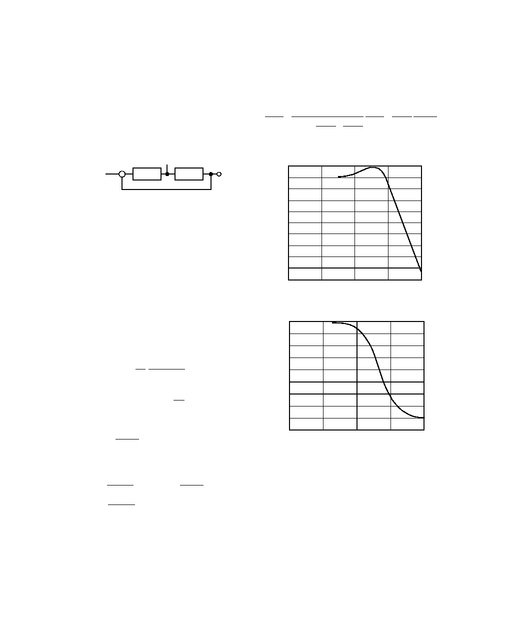
The normalized gain and phase diagrams are given in Figures 10
and 11 with a bandwidth of 1.25 kHz.
5
45
10k
30
40
10
35
1
15
25
20
10
5
0
1k
100
FREQUENCY Hz
Figure 10. AD2S93 Gain Plot
180
140
160
120
100
60
40
FREQUENCY Hz
0
10k
10
1
80
20
1k
100
Figure 11. AD2S93 Phase Plot
CIRCUIT DYNAMICS/ERROR SOURCES
TRANSFER FUNCTION
The AD2S93 operates as a Type 2 tracking servo loop. An inte-
grator and VCO/counter perform the two integrations inherent
in a Type 2 loop.
The overall system response of the AD2S93 is that of a unity
gain second order low-pass filter, with the position of the LVDT
as the input and the digital position data as the output. Figure 9
illustrates the AD2S93 system diagram.
G1 (s)
G2 (s)
VEL OUT
OUT
IN
+
Figure 9. AD2S93 Transfer Function
Note: The AD2S93 has been configured with the following dy-
namics.
Reference Frequency
10 kHz
3 dB Bandwidth
1250 Hz
VCO Gain is set in MODE 1 where VCOGAIN is connected to
VEL.
Using the procedure described in "SETTING THE CON-
VERTER BANDWIDTH," the following preferred values (E12
series) were calculated:
C1 = 820 pF
C2 = 6.8 nF
R2 = 56 k
C3 = C4 = 470 pF, R7 = 15 k
, R5 = R6 = 33 k
, C4 =
470 pF
The open-loop transfer function is given by:
G1(s)
=
K
1
s
1
+
st
1
1
+
st
2
G2(s)
=
K
2
s
where:
t
2
=
R
2
C
1
×
C
2
C
1
+
C
2
t
1
= R
2
C
2
and:
K
1
=
4
×
10
-
3
25
×
10
3
=
160
×
10
-
9
×
1
C
1
+
C
2
=
21
K
2
=
4
R
V
×
C
V
Note A
2
has two values depending on which mode is being used
K
2
(MODE1)
= 640
×
10
3
K
2
(MODE2)
= 160
×
10
3
The AD2S93 acceleration constant is given by:
K
a
= K
1
×
K
2
Therefore in the example given,
K
a
= K
1
×
K
2
= 21
×
640
×
10
3
= 13.44
×
10
6
s
2
11
REV. A
AD2S93
The small step response is given in Figure 12, and is the time
taken for the converter to settled to within 1 LSB.
ts = 7 ms (14-bit resolution)
The large step response (steps >5% of FSR) applies when the
error voltage will exceed the linear range of the converter. Typi-
cally it will take three times longer to reach the first peak FSR.
In response to a velocity step [VELOUT/(d
/dt)] the velocity
output will exhibit the same response characteristics as outlined
above.
20
0
0
2%FS
16
12
8
4
POSITION
Figure 12. Small Step Response
SOURCES OF ERROR
ACCELERATION ERROR
A tracking converter employing a Type 2 servo loop does not
suffer any velocity lag, however, there is an additional error due
to acceleration. This additional error can be defined using the
acceleration constant K
a
of the converter.
K
a
=
input acceleration
position
The numerator and denominator's units must be consistent.
K
a
does not define maximum input acceleration, only the error due
to its acceleration. The maximum acceleration allowable before
the converter loses track is dependent on the positional accuracy
requirement of the system.
Position Error
×
K
a
= LSB/sec
2
K
a
can be used to predict the output position error for a
given input acceleration. The AD2S93 in the example has
a K
a
= 13.44
×
10
6
sec
-2
if we apply an input accelerating at
100
×
2
14
LSB/sec
2
.
Error in LSBs =
input acceleration LSB/ sec
2
[
]
K
a
sec
-2
[
]
=
100
×
2
14
13.44
×
10
6
=
0.12 LSBs
12
C1881281/94
PRINTED IN U.S.A.
OUTLINE DIMENSIONS
Dimensions shown in inches and (mm).
P-28A
0.048 (1.21)
0.042 (1.07)
0.456 (11.58)
0.450 (11.43)
SQ
0.495 (12.57)
0.485 (12.32)
SQ
0.048 (1.21)
0.042 (1.07)
0.050
(1.27)
BSC
26
4
TOP VIEW
25
19
12
11
PIN 1
IDENTIFIER
5
18
0.020
(0.50)
R
0.032 (0.81)
0.026 (0.66)
0.021 (0.53)
0.013 (0.33)
0.056 (1.42)
0.042 (1.07)
0.025 (0.63)
0.015 (0.38)
0.180 (4.57)
0.165 (4.19)
0.430 (10.92)
0.390 (9.91)
0.110 (2.79)
0.085 (2.16)
0.040 (1.01)
0.025 (0.64)
Document Outline
- Specifications
- Package drawings
- Ordering Guide
- Features
- Applications
- Product Description
- Timing characteristics
- Absolute Maximum Ratings
- Functional Block Diagram
- Pin Function Description
- PRODUCT HIGHLIGHTS
- RECOMMENDED OPERATING CONDITIONS
- GLOSSARY OF TERMS
- PRINCIPLE OF OPERATION
- DATA FORMAT
- OPERATING RANGE
- SCALING THE INPUTS
- INPUT GAIN
- SETTING THE CONVERTER BANDWIDTH
- INTERFACING TO THE AD2S93
- IN-BUILT DIAGNOSTICS
- CONNECTING THE CONVERTER
- CALCULATING HF FILTER (C3, C4, R5, R6)
- PHASE SHIFT AND QUADRATURE EFFECTS
- REMOTE MULTIPLE SENSOR INTERFACING
- CIRCUIT DYNAMICS/ERROR SOURCES TRANSFER FUNCTION
- SOURCES OF ERROR
- ACCELERATION ERROR
- DIAGRAMS
- Timing Diagram
- Functional Block Diagram
- Pre-Amp Gain Block
- Integrator and VCO
- Half-Bridge Type LVDT Connection
- Three- or Four-Wire LVDT Connection
- Two-Wire LVDT Connection
- Remote Sensor Interface
- Transfer Function